Tag Archives: Mott memristor

Geoffrey Hinton (University of Toronto) shares 2024 Nobel Prize for Physics with John J. Hopfield (Princeton University)

What an interesting choice the committee deciding on the 2024 Nobel Prize for Physics have made. Geoffrey Hinton has been mentioned here a number of times, most recently for his participation in one of the periodic AI (artificial intelligence) panics that pop up from time to time. For more about the latest one and Hinton’s participation see my May 25, 2023 posting “Non-human authors (ChatGPT or others) of scientific and medical studies and the latest AI panic!!!” and scroll down to ‘The panic’ subhead.

I have almost nothing about John J. Hopfield other than a tangential mention of the Hopfield neural network in a January 3, 2018 posting “Mott memristor.”

An October 8, 2024 Royal Swedish Academy of Sciences press release announces the winners of the 2024 Nobel Prize in Physics,

The Royal Swedish Academy of Sciences has decided to award the Nobel Prize in Physics 2024 to

John J. Hopfield
Princeton University, NJ, USA

Geoffrey E. Hinton
University of Toronto, Canada

“for foundational discoveries and inventions that enable machine learning with artificial neural networks”

They trained artificial neural networks using physics

This year’s two Nobel Laureates in Physics have used tools from physics to develop methods that are the foundation of today’s powerful machine learning. John Hopfield created an associative memory that can store and reconstruct images and other types of patterns in data. Geoffrey Hinton invented a method that can autonomously find properties in data, and so perform tasks such as identifying specific elements in pictures.

When we talk about artificial intelligence, we often mean machine learning using artificial neural networks. This technology was originally inspired by the structure of the brain. In an artificial neural network, the brain’s neurons are represented by nodes that have different values. These nodes influence each other through con­nections that can be likened to synapses and which can be made stronger or weaker. The network is trained, for example by developing stronger connections between nodes with simultaneously high values. This year’s laureates have conducted important work with artificial neural networks from the 1980s onward.

John Hopfield invented a network that uses a method for saving and recreating patterns. We can imagine the nodes as pixels. The Hopfield network utilises physics that describes a material’s characteristics due to its atomic spin – a property that makes each atom a tiny magnet. The network as a whole is described in a manner equivalent to the energy in the spin system found in physics, and is trained by finding values for the connections between the nodes so that the saved images have low energy. When the Hopfield network is fed a distorted or incomplete image, it methodically works through the nodes and updates their values so the network’s energy falls. The network thus works stepwise to find the saved image that is most like the imperfect one it was fed with.

Geoffrey Hinton used the Hopfield network as the foundation for a new network that uses a different method: the Boltzmann machine. This can learn to recognise characteristic elements in a given type of data. Hinton used tools from statistical physics, the science of systems built from many similar components. The machine is trained by feeding it examples that are very likely to arise when the machine is run. The Boltzmann machine can be used to classify images or create new examples of the type of pattern on which it was trained. Hinton has built upon this work, helping initiate the current explosive development of machine learning.

“The laureates’ work has already been of the greatest benefit. In physics we use artificial neural networks in a vast range of areas, such as developing new materials with specific properties,” says Ellen Moons, Chair of the Nobel Committee for Physics.

An October 8, 2024 University of Toronto news release by Rahul Kalvapalle provides more detail about Hinton’s work and history with the university.

Ben Edwards wrote an October 8, 2024 article for Ars Technica, which in addition to reiterating the announcement explores a ‘controversial’ element to the story, Note 1: I gather I’m not the only one who found the award of a physics prize to researchers in the field of computer science a little unusual, Note 2: Links have been removed,

Hopfield and Hinton’s research, which dates back to the early 1980s, applied principles from physics to develop methods that underpin modern machine-learning techniques. Their work has enabled computers to perform tasks such as image recognition and pattern completion, capabilities that are now ubiquitous in everyday technology.

The win is already turning heads on social media because it seems unusual that research in a computer science field like machine learning might win a Nobel Prize for physics. “And the 2024 Nobel Prize in Physics does not go to physics…” tweeted German physicist Sabine Hossenfelder this morning [October 8, 2024].

From the Nobel committee’s point of view, the award largely derives from the fact that the two men drew from statistical models used in physics and partly from recognizing the advancements in physics research that came from using the men’s neural network techniques as research tools.

Nobel committee chair Ellen Moons, a physicist at Karlstad University, Sweden, said during the announcement, “Artificial neural networks have been used to advance research across physics topics as diverse as particle physics, material science and astrophysics.”

For a comprehensive overview of both Nobel prize winners, Hinton and Hopfield, their work, and their stands vis à vis the dangers of AI, there’s an October 8, 2024 Associated Press article on phys.org.

New path to viable memristor/neuristor?

I first stumbled onto memristors and the possibility of brain-like computing sometime in 2008 (around the time that R. Stanley Williams and his team at HP Labs first published the results of their research linking Dr. Leon Chua’s memristor theory to their attempts to shrink computer chips). In the almost 10 years since, scientists have worked hard to utilize memristors in the field of neuromorphic (brain-like) engineering/computing.

A January 22, 2018 news item on phys.org describes the latest work,

When it comes to processing power, the human brain just can’t be beat.

Packed within the squishy, football-sized organ are somewhere around 100 billion neurons. At any given moment, a single neuron can relay instructions to thousands of other neurons via synapses—the spaces between neurons, across which neurotransmitters are exchanged. There are more than 100 trillion synapses that mediate neuron signaling in the brain, strengthening some connections while pruning others, in a process that enables the brain to recognize patterns, remember facts, and carry out other learning tasks, at lightning speeds.

Researchers in the emerging field of “neuromorphic computing” have attempted to design computer chips that work like the human brain. Instead of carrying out computations based on binary, on/off signaling, like digital chips do today, the elements of a “brain on a chip” would work in an analog fashion, exchanging a gradient of signals, or “weights,” much like neurons that activate in various ways depending on the type and number of ions that flow across a synapse.

In this way, small neuromorphic chips could, like the brain, efficiently process millions of streams of parallel computations that are currently only possible with large banks of supercomputers. But one significant hangup on the way to such portable artificial intelligence has been the neural synapse, which has been particularly tricky to reproduce in hardware.

Now engineers at MIT [Massachusetts Institute of Technology] have designed an artificial synapse in such a way that they can precisely control the strength of an electric current flowing across it, similar to the way ions flow between neurons. The team has built a small chip with artificial synapses, made from silicon germanium. In simulations, the researchers found that the chip and its synapses could be used to recognize samples of handwriting, with 95 percent accuracy.

A January 22, 2018 MIT news release by Jennifer Chua (also on EurekAlert), which originated the news item, provides more detail about the research,

The design, published today [January 22, 2018] in the journal Nature Materials, is a major step toward building portable, low-power neuromorphic chips for use in pattern recognition and other learning tasks.

The research was led by Jeehwan Kim, the Class of 1947 Career Development Assistant Professor in the departments of Mechanical Engineering and Materials Science and Engineering, and a principal investigator in MIT’s Research Laboratory of Electronics and Microsystems Technology Laboratories. His co-authors are Shinhyun Choi (first author), Scott Tan (co-first author), Zefan Li, Yunjo Kim, Chanyeol Choi, and Hanwool Yeon of MIT, along with Pai-Yu Chen and Shimeng Yu of Arizona State University.

Too many paths

Most neuromorphic chip designs attempt to emulate the synaptic connection between neurons using two conductive layers separated by a “switching medium,” or synapse-like space. When a voltage is applied, ions should move in the switching medium to create conductive filaments, similarly to how the “weight” of a synapse changes.

But it’s been difficult to control the flow of ions in existing designs. Kim says that’s because most switching mediums, made of amorphous materials, have unlimited possible paths through which ions can travel — a bit like Pachinko, a mechanical arcade game that funnels small steel balls down through a series of pins and levers, which act to either divert or direct the balls out of the machine.

Like Pachinko, existing switching mediums contain multiple paths that make it difficult to predict where ions will make it through. Kim says that can create unwanted nonuniformity in a synapse’s performance.

“Once you apply some voltage to represent some data with your artificial neuron, you have to erase and be able to write it again in the exact same way,” Kim says. “But in an amorphous solid, when you write again, the ions go in different directions because there are lots of defects. This stream is changing, and it’s hard to control. That’s the biggest problem — nonuniformity of the artificial synapse.”

A perfect mismatch

Instead of using amorphous materials as an artificial synapse, Kim and his colleagues looked to single-crystalline silicon, a defect-free conducting material made from atoms arranged in a continuously ordered alignment. The team sought to create a precise, one-dimensional line defect, or dislocation, through the silicon, through which ions could predictably flow.

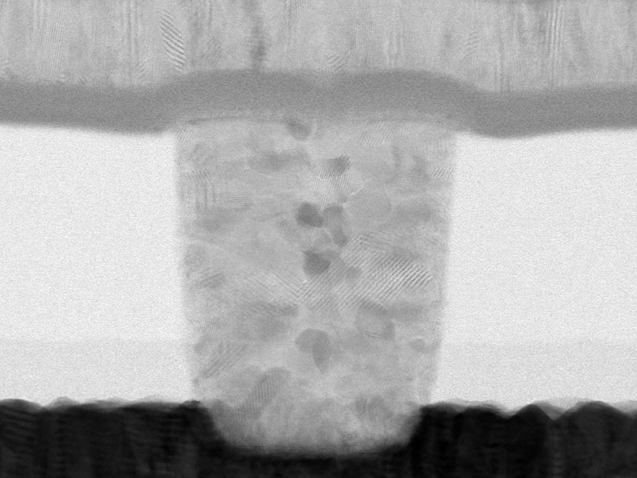
To do so, the researchers started with a wafer of silicon, resembling, at microscopic resolution, a chicken-wire pattern. They then grew a similar pattern of silicon germanium — a material also used commonly in transistors — on top of the silicon wafer. Silicon germanium’s lattice is slightly larger than that of silicon, and Kim found that together, the two perfectly mismatched materials can form a funnel-like dislocation, creating a single path through which ions can flow.

The researchers fabricated a neuromorphic chip consisting of artificial synapses made from silicon germanium, each synapse measuring about 25 nanometers across. They applied voltage to each synapse and found that all synapses exhibited more or less the same current, or flow of ions, with about a 4 percent variation between synapses — a much more uniform performance compared with synapses made from amorphous material.

They also tested a single synapse over multiple trials, applying the same voltage over 700 cycles, and found the synapse exhibited the same current, with just 1 percent variation from cycle to cycle.

“This is the most uniform device we could achieve, which is the key to demonstrating artificial neural networks,” Kim says.

Writing, recognized

As a final test, Kim’s team explored how its device would perform if it were to carry out actual learning tasks — specifically, recognizing samples of handwriting, which researchers consider to be a first practical test for neuromorphic chips. Such chips would consist of “input/hidden/output neurons,” each connected to other “neurons” via filament-based artificial synapses.

Scientists believe such stacks of neural nets can be made to “learn.” For instance, when fed an input that is a handwritten ‘1,’ with an output that labels it as ‘1,’ certain output neurons will be activated by input neurons and weights from an artificial synapse. When more examples of handwritten ‘1s’ are fed into the same chip, the same output neurons may be activated when they sense similar features between different samples of the same letter, thus “learning” in a fashion similar to what the brain does.

Kim and his colleagues ran a computer simulation of an artificial neural network consisting of three sheets of neural layers connected via two layers of artificial synapses, the properties of which they based on measurements from their actual neuromorphic chip. They fed into their simulation tens of thousands of samples from a handwritten recognition dataset commonly used by neuromorphic designers, and found that their neural network hardware recognized handwritten samples 95 percent of the time, compared to the 97 percent accuracy of existing software algorithms.

The team is in the process of fabricating a working neuromorphic chip that can carry out handwriting-recognition tasks, not in simulation but in reality. Looking beyond handwriting, Kim says the team’s artificial synapse design will enable much smaller, portable neural network devices that can perform complex computations that currently are only possible with large supercomputers.

“Ultimately we want a chip as big as a fingernail to replace one big supercomputer,” Kim says. “This opens a stepping stone to produce real artificial hardware.”

This research was supported in part by the National Science Foundation.

Here’s a link to and a citation for the paper,

SiGe epitaxial memory for neuromorphic computing with reproducible high performance based on engineered dislocations by Shinhyun Choi, Scott H. Tan, Zefan Li, Yunjo Kim, Chanyeol Choi, Pai-Yu Chen, Hanwool Yeon, Shimeng Yu, & Jeehwan Kim. Nature Materials (2018) doi:10.1038/s41563-017-0001-5 Published online: 22 January 2018

This paper is behind a paywall.

For the curious I have included a number of links to recent ‘memristor’ postings here,

January 22, 2018: Memristors at Masdar

January 3, 2018: Mott memristor

August 24, 2017: Neuristors and brainlike computing

June 28, 2017: Dr. Wei Lu and bio-inspired ‘memristor’ chips

May 2, 2017: Predicting how a memristor functions

December 30, 2016: Changing synaptic connectivity with a memristor

December 5, 2016: The memristor as computing device

November 1, 2016: The memristor as the ‘missing link’ in bioelectronic medicine?

You can find more by using ‘memristor’ as the search term in the blog search function or on the search engine of your choice.

Mott memristor

Mott memristors (mentioned in my Aug. 24, 2017 posting about neuristors and brainlike computing) gets more fulsome treatment in an Oct. 9, 2017 posting by Samuel K. Moore on the Nanoclast blog (found on the IEEE [Institute of Electrical and Electronics Engineers] website) Note: 1: Links have been removed; Note 2 : I quite like Moore’s writing style but he’s not for the impatient reader,

When you’re really harried, you probably feel like your head is brimful of chaos. You’re pretty close. Neuroscientists say your brain operates in a regime termed the “edge of chaos,” and it’s actually a good thing. It’s a state that allows for fast, efficient analog computation of the kind that can solve problems that grow vastly more difficult as they become bigger in size.

The trouble is, if you’re trying to replicate that kind of chaotic computation with electronics, you need an element that both acts chaotically—how and when you want it to—and could scale up to form a big system.

“No one had been able to show chaotic dynamics in a single scalable electronic device,” says Suhas Kumar, a researcher at Hewlett Packard Labs, in Palo Alto, Calif. Until now, that is.

He, John Paul Strachan, and R. Stanley Williams recently reported in the journal Nature that a particular configuration of a certain type of memristor contains that seed of controlled chaos. What’s more, when they simulated wiring these up into a type of circuit called a Hopfield neural network, the circuit was capable of solving a ridiculously difficult problem—1,000 instances of the traveling salesman problem—at a rate of 10 trillion operations per second per watt.

(It’s not an apples-to-apples comparison, but the world’s most powerful supercomputer as of June 2017 managed 93,015 trillion floating point operations per second but consumed 15 megawatts doing it. So about 6 billion operations per second per watt.)

The device in question is called a Mott memristor. Memristors generally are devices that hold a memory, in the form of resistance, of the current that has flowed through them. The most familiar type is called resistive RAM (or ReRAM or RRAM, depending on who’s asking). Mott memristors have an added ability in that they can also reflect a temperature-driven change in resistance.

The HP Labs team made their memristor from an 8-nanometer-thick layer of niobium dioxide (NbO2) sandwiched between two layers of titanium nitride. The bottom titanium nitride layer was in the form of a 70-nanometer wide pillar. “We showed that this type of memristor can generate chaotic and nonchaotic signals,” says Williams, who invented the memristor based on theory by Leon Chua.

(The traveling salesman problem is one of these. In it, the salesman must find the shortest route that lets him visit all of his customers’ cities, without going through any of them twice. It’s a difficult problem because it becomes exponentially more difficult to solve with each city you add.)

Here’s what the niobium dioxide-based Mott memristor looks like,

Photo: Suhas Kumar/Hewlett Packard Labs
A micrograph shows the construction of a Mott memristor composed of an 8-nanometer-thick layer of niobium dioxide between two layers of titanium nitride.

Here’s a link to and a citation for the paper,

Chaotic dynamics in nanoscale NbO2 Mott memristors for analogue computing by Suhas Kumar, John Paul Strachan & R. Stanley Williams. Nature 548, 318–321 (17 August 2017) doi:10.1038/nature23307 Published online: 09 August 2017

This paper is behind a paywall.