The Institut national de la recherche scientifique (INRS; Québec, Canada) has issued a January 30,2024 news release (also on EurekAlert) announcing new work in the field of imaging, Note: Links have been removed,
Teams led by professors Jinyang Liang and Fiorenzo Vetrone from the Énergie Matériaux Télécommunications Research Centre at the Institut national de la recherche scientifique (INRS) have developed a new system for imaging nanoparticles. It consists of a high-precision, short-wave infrared imaging technique capable of capturing the photoluminescence lifetimes of rare-earth doped nanoparticles in the micro- to millisecond range.
This groundbreaking discovery, which was published in the journal Advanced Science, paves the way for promising applications, particularly in the biomedical and information security fields.
Rare-earth elements are strategic metals that possess unique light-emitting properties that make them very attractive research tools in cutting-edge science. What’s more, the photoluminescence lifetime of nanoparticles doped with these ions has the advantage of being minimally affected by external conditions. As a result, measuring it through imaging provides data from which accurate and highly reliable information can be derived.
Although this field is seeing remarkable progress, existing optical systems for this type of measurement were less than ideal.
“Until now, existing optical systems have offered limited possibilities due to inefficient photon detection, limited imaging speed, and low sensitivity,” explains Professor Jinyang Liang, a specialist in ultrafast imaging and biophotonics.
To date, the most common technique for measuring the photoluminescence lifetime of rare-earth doped nanoparticles has involved counting time-correlated single photons.
“This method requires a large number of repeated excitations at the same location because the detector can only process a limited number of photons for each excitation,” says the study’s first author Miao Liu, a Ph.D. student in energy and materials science supervised by Profs. Liang and Vetrone.
However, the long photoluminescence lifetimes of rare-earth doped nanoparticles in the infrared spectrum, from hundreds of microseconds to several milliseconds, restrict the excitation’s repetition rate. As a result, the pixel dwelling time needed to build the photoluminescence intensity decay curve is much longer.
Pushing the limits
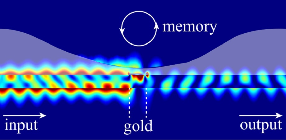
To overcome this challenge, Liang and Vetrone’s teams have combined streak optics with a high-sensitivity camera. The resulting device is called SWIR-PLIMASC (SWIR for short-wave infrared and PLIMASC for photoluminescence lifetime imaging microscopy using an all-optical streak camera). It vastly improves mapping of the optical properties of short-wave infrared photoluminescence lifetimes. It is the first high-sensitivity, high-speed SWIR imaging system in the optics field.
“It has several advantages,” says Miao Liu. “For instance, it responds to a wide spectral range, from 900 nm to 1700 nm, allowing photoluminescence to be detected at different wavelengths and/or spectral bands.”
The Ph.D. student adds that with the help of this device, photoluminescence lifetimes in the infrared spectrum, from microseconds to milliseconds, can be directly captured in one snapshot with a 1D imaging speed that can be tuned from 10.3 kHz to 138.9 kHz.
Finally, the operation that allocates the temporal information of photoluminescence to different spatial positions ensures that the entire process of 1D photoluminescence intensity decay can be recorded in a single snapshot, without repeated excitation. “You save time, but still get high sensitivity,” sums up Miao Liu.
Biomedical and security applications
The work carried out as part of this research will have a very tangible impact. In the biomedical field, the advances made possible by SWIR-PLIMASC could be used to fight cancer, believes Professor Fiorenzo Vetrone, whose expertise lies in nanomedicine.
“As our system applies to the temperature-based photoluminescence lifetime imaging of rare-earth ions, we believe that the data obtained could, for example, help to detect cancer cells even earlier and more accurately. The metabolism of those cells raises the temperature of the surrounding tissues,” says Professor Vetrone.
The innovative system can also be used to store information at enhanced security levels, more specifically to prevent documents and data from being falsified. Finally, in fundamental science, these unprecedented results will allow scientists to synthesize rare-earth nanoparticles with even more interesting optical properties.
Here’s a link to and a citation for the paper,
Short-wave Infrared Photoluminescence Lifetime Mapping of Rare-Earth Doped Nanoparticles Using All-Optical Streak Imaging by Miao Liu, Yingming Lai, Miguel Marquez, Fiorenzo Vetrone, Jinyang Liang. Advanced Science DOI: https://doi.org/10.1002/advs.202305284 First published: 06 January 2024
This paper is open access.