Tag Archives: diamonds

Stretching diamonds to improve electronic devices

On the last day of 2020, City University of Hong Kong (CityU) announced a technique for stretching diamonds that could result in a new generation of electronic devices. A December 31, 2020 news item on ScienceDaily makes the announcement,

Diamond is the hardest material in nature. It also has great potential as an excellent electronic material. A research team has demonstrated for the first time the large, uniform tensile elastic straining of microfabricated diamond arrays through the nanomechanical approach. Their findings have shown the potential of strained diamonds as prime candidates for advanced functional devices in microelectronics, photonics, and quantum information technologies.

A December 31, 2020 CityU press release on EurekAlert , which originated the news item, delves further into the research,

The research was co-led by Dr Lu Yang, Associate Professor in the Department of Mechanical Engineering (MNE) at CityU and researchers from Massachusetts Institute of Technology (MIT) and Harbin Institute of Technology (HIT). Their findings have been recently published in the prestigious scientific journal Science, titled “Achieving large uniform tensile elasticity in microfabricated diamond“.

“This is the first time showing the extremely large, uniform elasticity of diamond by tensile experiments. Our findings demonstrate the possibility of developing electronic devices through ‘deep elastic strain engineering’ of microfabricated diamond structures,” said Dr Lu.

Diamond: “Mount Everest” of electronic materials

Well known for its hardness, industrial applications of diamonds are usually cutting, drilling, or grinding. But diamond is also considered as a high-performance electronic and photonic material due to its ultra-high thermal conductivity, exceptional electric charge carrier mobility, high breakdown strength and ultra-wide bandgap. Bandgap is a key property in semi-conductor, and wide bandgap allows operation of high-power or high-frequency devices. “That’s why diamond can be considered as ‘Mount Everest’ of electronic materials, possessing all these excellent properties,” Dr Lu said.

However, the large bandgap and tight crystal structure of diamond make it difficult to “dope”, a common way to modulate the semi-conductors’ electronic properties during production, hence hampering the diamond’s industrial application in electronic and optoelectronic devices. A potential alternative is by “strain engineering”, that is to apply very large lattice strain, to change the electronic band structure and associated functional properties. But it was considered as “impossible” for diamond due to its extremely high hardness.

Then in 2018, Dr Lu and his collaborators discovered that, surprisingly, nanoscale diamond can be elastically bent with unexpected large local strain. This discovery suggests the change of physical properties in diamond through elastic strain engineering can be possible. Based on this, the latest study showed how this phenomenon can be utilized for developing functional diamond devices.

Uniform tensile straining across the sample

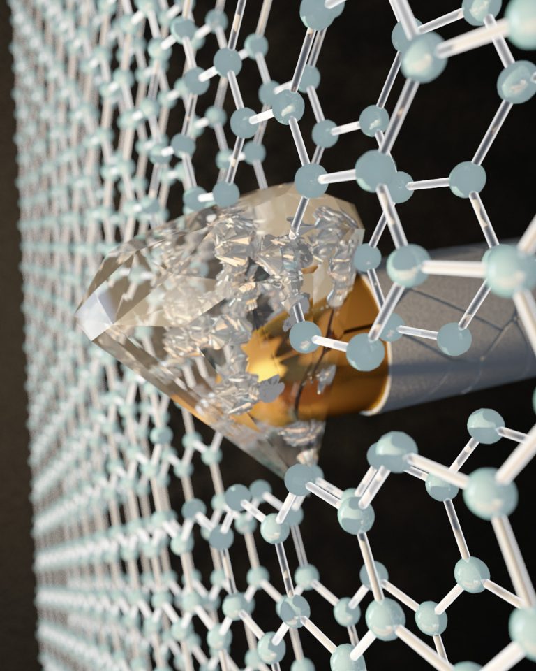
The team firstly microfabricated single-crystalline diamond samples from a solid diamond single crystals. The samples were in bridge-like shape – about one micrometre long and 300 nanometres wide, with both ends wider for gripping (See image: Tensile straining of diamond bridges). The diamond bridges were then uniaxially stretched in a well-controlled manner within an electron microscope. Under cycles of continuous and controllable loading-unloading of quantitative tensile tests, the diamond bridges demonstrated a highly uniform, large elastic deformation of about 7.5% strain across the whole gauge section of the specimen, rather than deforming at a localized area in bending. And they recovered their original shape after unloading.

By further optimizing the sample geometry using the American Society for Testing and Materials (ASTM) standard, they achieved a maximum uniform tensile strain of up to 9.7%, which even surpassed the maximum local value in the 2018 study, and was close to the theoretical elastic limit of diamond. More importantly, to demonstrate the strained diamond device concept, the team also realized elastic straining of microfabricated diamond arrays.

Tuning the bandgap by elastic strains

The team then performed density functional theory (DFT) calculations to estimate the impact of elastic straining from 0 to 12% on the diamond’s electronic properties. The simulation results indicated that the bandgap of diamond generally decreased as the tensile strain increased, with the largest bandgap reduction rate down from about 5 eV to 3 eV at around 9% strain along a specific crystalline orientation. The team performed an electron energy-loss spectroscopy analysis on a pre-strained diamond sample and verified this bandgap decreasing trend.

Their calculation results also showed that, interestingly, the bandgap could change from indirect to direct with the tensile strains larger than 9% along another crystalline orientation. Direct bandgap in semi-conductor means an electron can directly emit a photon, allowing many optoelectronic applications with higher efficiency.

These findings are an early step in achieving deep elastic strain engineering of microfabricated diamonds. By nanomechanical approach, the team demonstrated that the diamond’s band structure can be changed, and more importantly, these changes can be continuous and reversible, allowing different applications, from micro/nanoelectromechanical systems (MEMS/NEMS), strain-engineered transistors, to novel optoelectronic and quantum technologies. “I believe a new era for diamond is ahead of us,” said Dr Lu.

Here’s an illustration provided by the researchers,

Caption: Stretching of microfabricated diamonds pave ways for applications in next-generation microelectronics.. Credit: Dang Chaoqun / City University of Hong Kong

Here’s a link to and a citation for the paper,

Achieving large uniform tensile elasticity in microfabricated diamond by Chaoqun Dang, Jyh-Pin Chou, Bing Dai, Chang-Ti Chou, Yang Yang, Rong Fan, Weitong Lin, Fanling Meng, Alice Hu, Jiaqi Zhu, Jiecai Han, Andrew M. Minor, Ju Li, Yang Lu. Science 01 Jan 2021: Vol. 371, Issue 6524, pp. 76-78 DOI: 10.1126/science.abc4174

This paper is behind a paywall.

Using sound to transfer quantum information

It seems sound is becoming more prominent as a means of science data communication (data sonification) and in this upcoming case, data transfer. From a June 5, 2018 news item on ScienceDaily,

Quantum physics is on the brink of a technological breakthrough: new types of sensors, secure data transmission methods and maybe even computers could be made possible thanks to quantum technologies. However, the main obstacle here is finding the right way to couple and precisely control a sufficient number of quantum systems (for example, individual atoms).

A team of researchers from TU Wien and Harvard University has found a new way to transfer the necessary quantum information. They propose using tiny mechanical vibrations. The atoms are coupled with each other by ‘phonons’ — the smallest quantum mechanical units of vibrations or sound waves.

A June 5, 2018 Technical University of Vienna (TU Wien) press release, which originated the news item, explains the work in greater detail,

“We are testing tiny diamonds with built-in silicon atoms – these quantum systems are particularly promising,” says Professor Peter Rabl from TU Wien. “Normally, diamonds are made exclusively of carbon, but adding silicon atoms in certain places creates defects in the crystal lattice where quantum information can be stored.” These microscopic flaws in the crystal lattice can be used like a tiny switch that can be switched between a state of higher energy and a state of lower energy using microwaves.

Together with a team from Harvard University, Peter Rabl’s research group has developed a new idea to achieve the targeted coupling of these quantum memories within the diamond. One by one they can be built into a tiny diamond rod measuring only a few micrometres in length, like individual pearls on a necklace. Just like a tuning fork, this rod can then be made to vibrate – however, these vibrations are so small that they can only be described using quantum theory. It is through these vibrations that the silicon atoms can form a quantum-mechanical link to each other.

“Light is made from photons, the quantum of light. In the same way, mechanical vibrations or sound waves can also be described in a quantum-mechanical manner. They are comprised of phonons – the smallest possible units of mechanical vibration,” explains Peter Rabl. As the research team has now been able to show using simulation calculations, any number of these quantum memories can be linked together in the diamond rod thanks to these phonons. The individual silicon atoms are “switched on and off” using microwaves. During this process, they emit or absorb phonons. This creates a quantum entanglement of different silicon defects, thus allowing quantum information to be transferred.

The road to a scalable quantum network
Until now it was not clear whether something like this was even possible: “Usually you would expect the phonons to be absorbed somewhere, or to come into contact with the environment and thus lose their quantum mechanical properties,” says Peter Rabl. “Phonons are the enemy of quantum information, so to speak. But with our calculations, we were able to show that, when controlled appropriately using microwaves, the phonons are in fact useable for technical applications.”

The main advantage of this new technology lies in its scalability: “There are many ideas for quantum systems that, in principle, can be used for technological applications. The biggest problem is that it is very difficult to connect enough of them to be able to carry out complicated computing operations,” says Peter Rabl. The new strategy of using phonons for this purpose could pave the way to a scalable quantum technology.

Here’s a link to and a citation for the paper,

Phonon Networks with Silicon-Vacancy Centers in Diamond Waveguides by M.-A. Lemonde, S. Meesala, A. Sipahigil, M. J. A. Schuetz, M. D. Lukin, M. Loncar, and P. Rabl. Phys. Rev. Lett. 120 (21), 213603 DOI:https://doi.org/10.1103/PhysRevLett.120.213603 Published 25 May 2018

This paper is behind a paywall.

Bulletproof graphene

A December 18, 2017 news item on Nanowerk announces research that demonstrates graphene can be harder than diamonds (Note: A link has been removed),

Imagine a material as flexible and lightweight as foil that becomes stiff and hard enough to stop a bullet on impact. In a newly published paper in Nature Nanotechnology (“Ultrahard carbon film from epitaxial two-layer graphene”), researchers across The City University of New York (CUNY) describe a process for creating diamene: flexible, layered sheets of graphene that temporarily become harder than diamond and impenetrable upon impact.

Scientists at the Advanced Science Research Center (ASRC) at the Graduate Center, CUNY, worked to theorize and test how two layers of graphene — each one-atom thick — could be made to transform into a diamond-like material upon impact at room temperature. The team also found the moment of conversion resulted in a sudden reduction of electric current, suggesting diamene could have interesting electronic and spintronic properties. The new findings will likely have applications in developing wear-resistant protective coatings and ultra-light bullet-proof films.

A December 18, 2017 CUNY news release, which originated the news item, provides a little more detail,

“This is the thinnest film with the stiffness and hardness of diamond ever created,” said Elisa Riedo, professor of physics at the ASRC and the project’s lead researcher. “Previously, when we tested graphite or a single atomic layer of graphene, we would apply pressure and feel a very soft film. But when the graphite film was exactly two-layers thick, all of a sudden we realized that the material under pressure was becoming extremely hard and as stiff, or stiffer, than bulk diamond.”

Angelo Bongiorno, associate professor of chemistry at CUNY College of Staten Island and part of the research team, developed the theory for creating diamene. He and his colleagues used atomistic computer simulations to model potential outcomes when pressurizing two honeycomb layers of graphene aligned in different configurations. Riedo and other team members then used an atomic force microscope to apply localized pressure to two-layer graphene on silicon carbide substrates and found perfect agreement with the calculations. Experiments and theory both show that this graphite-diamond transition does not occur for more than two layers or for a single graphene layer.

“Graphite and diamonds are both made entirely of carbon, but the atoms are arranged differently in each material, giving them distinct properties such as hardness, flexibility and electrical conduction,” Bongiorno said. “Our new technique allows us to manipulate graphite so that it can take on the beneficial properties of a diamond under specific conditions.”

The research team’s successful work opens up possibilities for investigating graphite-to-diamond phase transition in two-dimensional materials, according to the paper. Future research could explore methods for stabilizing the transition and allow for further applications for the resulting materials.

There’s an artist’s representation of a bullet’s impact on graphene,

By applying pressure at the nanoscale with an indenter to two layers of graphene, each one-atom thick, CUNY researchers transformed the honeycombed graphene into a diamond-like material at room temperature. Photo credit: Ella Maru Studio Courtesy: CUNY

Here’s a link to and a citation for the paper,

Ultrahard carbon film from epitaxial two-layer graphene by Yang Gao, Tengfei Cao, Filippo Cellini, Claire Berger, Walter A. de Heer, Erio Tosatti, Elisa Riedo, & Angelo Bongiorno. Nature Nanotechnology (2017) doi:10.1038/s41565-017-0023-9 Published online: 18 December 2017

This paper is behind a paywall.

Formation of a time (temporal) crystal

It’s a crystal arranged in time according to a March 8, 2017 University of Texas at Austin news release (also on EurekAlert), Note: Links have been removed,

Salt, snowflakes and diamonds are all crystals, meaning their atoms are arranged in 3-D patterns that repeat. Today scientists are reporting in the journal Nature on the creation of a phase of matter, dubbed a time crystal, in which atoms move in a pattern that repeats in time rather than in space.

The atoms in a time crystal never settle down into what’s known as thermal equilibrium, a state in which they all have the same amount of heat. It’s one of the first examples of a broad new class of matter, called nonequilibrium phases, that have been predicted but until now have remained out of reach. Like explorers stepping onto an uncharted continent, physicists are eager to explore this exotic new realm.

“This opens the door to a whole new world of nonequilibrium phases,” says Andrew Potter, an assistant professor of physics at The University of Texas at Austin. “We’ve taken these theoretical ideas that we’ve been poking around for the last couple of years and actually built it in the laboratory. Hopefully, this is just the first example of these, with many more to come.”

Some of these nonequilibrium phases of matter may prove useful for storing or transferring information in quantum computers.

Potter is part of the team led by researchers at the University of Maryland who successfully created the first time crystal from ions, or electrically charged atoms, of the element ytterbium. By applying just the right electrical field, the researchers levitated 10 of these ions above a surface like a magician’s assistant. Next, they whacked the atoms with a laser pulse, causing them to flip head over heels. Then they hit them again and again in a regular rhythm. That set up a pattern of flips that repeated in time.

Crucially, Potter noted, the pattern of atom flips repeated only half as fast as the laser pulses. This would be like pounding on a bunch of piano keys twice a second and notes coming out only once a second. This weird quantum behavior was a signature that he and his colleagues predicted, and helped confirm that the result was indeed a time crystal.

The team also consists of researchers at the National Institute of Standards and Technology, the University of California, Berkeley and Harvard University, in addition to the University of Maryland and UT Austin.

Frank Wilczek, a Nobel Prize-winning physicist at the Massachusetts Institute of Technology, was teaching a class about crystals in 2012 when he wondered whether a phase of matter could be created such that its atoms move in a pattern that repeats in time, rather than just in space.

Potter and his colleague Norman Yao at UC Berkeley created a recipe for building such a time crystal and developed ways to confirm that, once you had built such a crystal, it was in fact the real deal. That theoretical work was announced publically last August and then published in January in the journal Physical Review Letters.

A team led by Chris Monroe of the University of Maryland in College Park built a time crystal, and Potter and Yao helped confirm that it indeed had the properties they predicted. The team announced that breakthrough—constructing a working time crystal—last September and is publishing the full, peer-reviewed description today in Nature.

A team led by Mikhail Lukin at Harvard University created a second time crystal a month after the first team, in that case, from a diamond.

Here’s a link to and a citation for the paper,

Observation of a discrete time crystal by J. Zhang, P. W. Hess, A. Kyprianidis, P. Becker, A. Lee, J. Smith, G. Pagano, I.-D. Potirniche, A. C. Potter, A. Vishwanath, N. Y. Yao, & C. Monroe. Nature 543, 217–220 (09 March 2017) doi:10.1038/nature21413 Published online 08 March 2017

This paper is behind a paywall.

Gold-144 is a polymorph

Au-144 (also known as Gold-144) is an iconic gold nanocluster according to a June 14, 2016 news item announcing its polymorphic nature on ScienceDaily,

Chemically the same, graphite and diamonds are as physically distinct as two minerals can be, one opaque and soft, the other translucent and hard. What makes them unique is their differing arrangement of carbon atoms.

Polymorphs, or materials with the same composition but different structures, are common in bulk materials, and now a new study in Nature Communications confirms they exist in nanomaterials, too. Researchers describe two unique structures for the iconic gold nanocluster Au144(SR)60, better known as Gold-144, including a version never seen before. Their discovery gives engineers a new material to explore, along with the possibility of finding other polymorphic nanoparticles.

A June 14, 2016 Columbia University news release (also on EurekAlert), which originated the news item, provides more insight into the work,

“This took four years to unravel,” said Simon Billinge, a physics professor at Columbia Engineering and a member of the Data Science Institute. “We weren’t expecting the clusters to take on more than one atomic arrangement. But this discovery gives us more handles to turn when trying to design clusters with new and useful properties.”

Gold has been used in coins and jewelry for thousands of years for its durability, but shrink it to a size 10,000 times smaller than a human hair [at one time one billionth of a meter or a nanometer was said to be 1/50,000, 1/60,000 or 1/100,000 of the diameter of a human hair], and it becomes wildly unstable and unpredictable. At the nanoscale, gold likes to split apart other particles and molecules, making it a useful material for purifying water, imaging and killing tumors, and making solar panels more efficient, among other applications.

Though a variety of nanogold particles and molecules have been made in the lab, very few have had their secret atomic arrangement revealed. But recently, new technologies are bringing these miniscule structures into focus.

Under one approach, high-energy x-ray beams are fired at a sample of nanoparticles. Advanced data analytics are used to interpret the x-ray scattering data and infer the sample’s structure, which is key to understanding how strong, reactive or durable the particles might be.

Billinge and his lab have pioneered a method, the atomic Pair Distribution Function (PDF) analysis, for interpreting this scattering data. To test the PDF method, Billinge asked chemists at the Colorado State University to make tiny samples of Gold-144, a molecule-sized nanogold cluster first isolated in 1995. Its structure had been theoretically predicted in 2009, and though never confirmed, Gold-144 has found numerous applications, including in tissue-imaging.

Hoping the test would confirm Gold-144’s structure, they analyzed the clusters at the European Synchrotron Radiation Source in Grenoble, and used the PDF method to infer their structure. To their surprise, they found an angular core, and not the sphere-like icosahedral core predicted. When they made a new sample and tried the experiment again, this time using synchrotrons at Brookhaven and Argonne national laboratories, the structure came back spherical.

“We didn’t understand what was going on, but digging deeper, we realized we had a polymorph,” said study coauthor Kirsten Jensen, formerly a postdoctoral researcher at Columbia, now a chemistry professor at the University of Copenhagen.

Further experiments confirmed the cluster had two versions, sometimes found together, each with a unique structure indicating they behave differently. The researchers are still unsure if Gold-144 can switch from one version to the other or, what exactly, differentiates the two forms.

To make their discovery, the researchers solved what physicists call the nanostructure inverse problem. How can the structure of a tiny nanoparticle in a sample be inferred from an x-ray signal that has been averaged over millions of particles, each with different orientations?

“The signal is noisy and highly degraded,” said Billinge. “It’s the equivalent of trying to recognize if the bird in the tree is a robin or a cardinal, but the image in your binoculars is too blurry and distorted to tell.”

“Our results demonstrate the power of PDF analysis to reveal the structure of very tiny particles,” added study coauthor Christopher Ackerson, a chemistry professor at Colorado State. “I’ve been trying, off and on, for more than 10 years to get the single-crystal x-ray structure of Gold-144. The presence of polymorphs helps to explain why this molecule has been so resistant to traditional methods.”

The PDF approach is one of several rival methods being developed to bring nanoparticle structure into focus. Now that it has proven itself, it could help speed up the work of describing other nanostructures.

The eventual goal is to design nanoparticles by their desired properties, rather than through trial and error, by understanding how form and function relate. Databases of known and predicted structures could make it possible to design new materials with a few clicks of a mouse.

The study is a first step.

“We’ve had a structure model for this iconic gold molecule for years and then this study comes along and says the structure is basically right but it’s got a doppelgänger,” said Robert Whetten, a professor of chemical physics at the University of Texas, San Antonio, who led the team that first isolated Gold-144. “It seemed preposterous, to have two distinct structures that underlie its ubiquity, but this is a beautiful paper that will persuade a lot of people.”

Here’s an image illustrating the two shapes,

Setting out to confirm the predicted structure of Gold-144, researchers discovered an entirely unexpected atomic arrangement (right). The two structures, described in detail for the first time, each have 144 gold atoms, but are uniquely shaped, suggesting they also behave differently. (Courtesy of Kirsten Ørnsbjerg Jensen)

Setting out to confirm the predicted structure of Gold-144, researchers discovered an entirely unexpected atomic arrangement (right). The two structures, described in detail for the first time, each have 144 gold atoms, but are uniquely shaped, suggesting they also behave differently. (Courtesy of Kirsten Ørnsbjerg Jensen)

Here’s a link to and a citation for the paper,

Polymorphism in magic-sized Au144(SR)60 clusters by Kirsten M.Ø. Jensen, Pavol Juhas, Marcus A. Tofanelli, Christine L. Heinecke, Gavin Vaughan, Christopher J. Ackerson, & Simon J. L. Billinge.  Nature Communications 7, Article number: 11859  doi:10.1038/ncomms11859 Published 14 June 2016

This is an open access paper.

Diamond-based electronics?

A May 24, 2016 news item on ScienceDaily describes the latest research on using diamonds as semiconductors,

Along with being a “girl’s best friend,” diamonds also have remarkable properties that could make them ideal semiconductors. This is welcome news for electronics; semiconductors are needed to meet the rising demand for more efficient electronics that deliver and convert power.

The thirst for electronics is unlikely to cease and almost every appliance or device requires a suite of electronics that transfer, convert and control power. Now, researchers have taken an important step toward that technology with a new way to dope single crystals of diamonds, a crucial process for building electronic devices.

A May 24, 2016 American Institute of Physics (AIP) news release (also on EurekAlert), which originated the news item, provides more detail,

For power electronics, diamonds could serve as the perfect material. They are thermally conductive, which means diamond-based devices would dissipate heat quickly and easily, foregoing the need for bulky and expensive methods for cooling. Diamond can also handle high voltages and power. Electrical currents also flow through diamonds quickly, meaning the material would make for energy efficient devices.

But among the biggest challenges to making diamond-based devices is doping, a process in which other elements are integrated into the semiconductor to change its properties. Because of diamond’s rigid crystalline structure, doping is difficult.

Currently, you can dope diamond by coating the crystal with boron and heating it to 1450 degrees Celsius. But it’s difficult to remove the boron coating at the end. This method only works on diamonds consisting of multiple crystals stuck together. Because such polydiamonds have irregularities between the crystals, single-crystals would be superior semiconductors.

You can dope single crystals by injecting boron atoms while growing the crystals artificially. The problem is the process requires powerful microwaves that can degrade the quality of the crystal.

Now, Ma [Zhengqiang (Jack) Ma, an electrical and computer engineering professor at the University of Wisconsin-Madison] and his colleagues have found a way to dope single-crystal diamonds with boron at relatively low temperatures and without any degradation. The researchers discovered if you bond a single-crystal diamond with a piece of silicon doped with boron, and heat it to 800 degrees Celsius, which is low compared to the conventional techniques, the boron atoms will migrate from the silicon to the diamond. It turns out that the boron-doped silicon has defects such as vacancies, where an atom is missing in the lattice structure. Carbon atoms from the diamond will fill those vacancies, leaving empty spots for boron atoms.

This technique also allows for selective doping, which means more control when making devices. You can choose where to dope a single-crystal diamond simply by bonding the silicon to that spot.

The new method only works for P-type doping, where the semiconductor is doped with an element that provides positive charge carriers (in this case, the absence of electrons, called holes).

“We feel like we found a very easy, inexpensive, and effective way to do it,” Ma said. The researchers are already working on a simple device using P-type single-crystal diamond semiconductors.

But to make electronic devices like transistors, you need N-type doping that gives the semiconductor negative charge carriers (electrons). And other barriers remain. Diamond is expensive and single crystals are very small.

Still, Ma says, achieving P-type doping is an important step, and might inspire others to find solutions for the remaining challenges. Eventually, he said, single-crystal diamond could be useful everywhere — perfect, for instance, for delivering power through the grid.

Here’s an image the researchers have released,

Optical image of a diode array on a natural single crystalline diamond plate. (The image looks blurred due to light scattering by the array of small pads on top of the diamond plate.) Inset shows the deposited anode metal on top of heavy doped Si nanomembrane that is bonded to natural single crystalline diamond. CREDIT: Jung-Hun Seo

Optical image of a diode array on a natural single crystalline diamond plate. (The image looks blurred due to light scattering by the array of small pads on top of the diamond plate.) Inset shows the deposited anode metal on top of heavy doped Si nanomembrane that is bonded to natural single crystalline diamond. CREDIT: Jung-Hun Seo Courtesy: American Institute of Physics

Here’s a link to and a citation for the paper,

Thermal diffusion boron doping of single-crystal natural diamond by Jung-Hun Seo, Henry Wu, Solomon Mikael, Hongyi Mi, James P. Blanchard, Giri Venkataramanan, Weidong Zhou, Shaoqin Gong, Dane Morgan, and Zhenqiang Ma. J. Appl. Phys. 119, 205703 (2016); http://dx.doi.org/10.1063/1.4949327

This paper appears to be open access.

South Africa, energy, and nanotechnology

South African academics Nosipho Moloto, Associate Professor, Department of Chemistry, University of the Witwatersrand and Siyabonga P. Ngubane, Lecturer in Chemistry, University of the Witwatersrand have written a Feb. 17, 2016 article for The Conversation (also available on the South African Broadcasting Corporation website) about South Africa’s energy needs and its nanotechnology efforts (Note: Links have been removed),

Energy is an economic driver of both developed and developing countries. South Africa over the past few years has faced an energy crisis with rolling blackouts between 2008 and 2015. Part of the problem has been attributed to mismanagement by the state-owned utility company Eskom, particularly the shortcomings of maintenance plans on several plants.

But South Africa has two things going for it that could help it out of its current crisis. By developing a strong nanotechnology capability and applying this to its rich mineral reserves the country is well-placed to develop new energy technologies.

Nanotechnology has already shown that it has the potential to alleviate energy problems. …

It can also yield materials with new properties and the miniaturisation of devices. For example, since the discovery of graphene, a single atomic layer of graphite, several applications in biological engineering, electronics and composite materials have been identified. These include economic and efficient devices like solar cells and lithium ion secondary batteries.

Nanotechnology has seen an incredible increase in commercialisation. Nearly 10,000 patents have been filed by large corporations since its beginning in 1991. There are already a number of nanotechnology products and solutions on the market. Examples include Miller’s beer bottling composites, Armor’s N-Force line bulletproof vests and printed solar cells produced by Nanosolar – as well as Samsung’s nanotechnology television.

The advent of nanotechnology in South Africa began with the South African Nanotechnology Initiative in 2002. This was followed by the a [sic] national nanotechnology strategy in 2003.

The government has spent more than R450 million [Rand] in nanotechnology and nanosciences research since 2006. For example, two national innovation centres have been set up and funding has been made available for equipment. There has also been flagship funding.

The country could be globally competitive in this field due to the infancy of the technology. As such, there are plenty of opportunities to make novel discoveries in South Africa.

Mineral wealth

There is another major advantage South Africa has that could help diversify its energy supply. It has an abundance of mineral wealth with an estimated value of US$2.5 trillion. The country has the world’s largest reserves of manganese and platinum group metals. It also has massive reserves of gold, diamonds, chromite ore and vanadium.

Through beneficiation and nanotechnology these resources could be used to cater for the development of new energy technologies. Research in beneficiation of minerals for energy applications is gaining momentum. For example, Anglo American and the Department of Science and Technology have embarked on a partnership to convert hydrogen into electricity.

The Council for Scientific and Industrial research also aims to develop low cost lithium ion batteries and supercapacitors using locally mined manganese and titanium ores. There is collaborative researchto use minerals like gold to synthesize nanomaterials for application in photovoltaics.

The current photovoltaic market relies on importing solar cells or panels from Europe, Asia and the US for local assembly to produce arrays. South African UV index is one of the highest in the world which reduces the lifespan of solar panels. The key to a thriving and profitable photovoltaic sector therefore lies in local production and research and development to support the sector.

It’s worth reading the article in its entirety if you’re interested in a perspective on South Africa’s energy and nanotechnology efforts.

Bejweled and bedazzled but not bewitched, bothered, or bewildered at Northwestern University

When discussing DNA (deoxyribonucleic acid) one doesn’t usually expect to encounter gems as one does in a Nov. 28, 2013 news item on Azonano,

Nature builds flawless diamonds, sapphires and other gems. Now a Northwestern University [located in Chicago, Illinois, US] research team is the first to build near-perfect single crystals out of nanoparticles and DNA, using the same structure favored by nature.

The Nov. 27, 2013 Northwestern University news release by Megan Fellman (also on EurekAlert), which originated the news item,, explains why single crystals are of such interest,

“Single crystals are the backbone of many things we rely on — diamonds for beauty as well as industrial applications, sapphires for lasers and silicon for electronics,” said nanoscientist Chad A. Mirkin. “The precise placement of atoms within a well-defined lattice defines these high-quality crystals.

“Now we can do the same with nanomaterials and DNA, the blueprint of life,” Mirkin said. “Our method could lead to novel technologies and even enable new industries, much as the ability to grow silicon in perfect crystalline arrangements made possible the multibillion-dollar semiconductor industry.”

His research group developed the “recipe” for using nanomaterials as atoms, DNA as bonds and a little heat to form tiny crystals. This single-crystal recipe builds on superlattice techniques Mirkin’s lab has been developing for nearly two decades.

(I wrote about Mirkin’s nanoparticle DNA work in the context of his proposed periodic table of modified nucleic acid nanoparticles in a July 5, 2013 posting.) The news release goes on to describe Mirkin’s most recent work,

In this recent work, Mirkin, an experimentalist, teamed up with Monica Olvera de la Cruz, a theoretician, to evaluate the new technique and develop an understanding of it. Given a set of nanoparticles and a specific type of DNA, Olvera de la Cruz showed they can accurately predict the 3-D structure, or crystal shape, into which the disordered components will self-assemble.

The general set of instructions gives researchers unprecedented control over the type and shape of crystals they can build. The Northwestern team worked with gold nanoparticles, but the recipe can be applied to a variety of materials, with potential applications in the fields of materials science, photonics, electronics and catalysis.

A single crystal has order: its crystal lattice is continuous and unbroken throughout. The absence of defects in the material can give these crystals unique mechanical, optical and electrical properties, making them very desirable.

In the Northwestern study, strands of complementary DNA act as bonds between disordered gold nanoparticles, transforming them into an orderly crystal. The researchers determined that the ratio of the DNA linker’s length to the size of the nanoparticle is critical.

“If you get the right ratio it makes a perfect crystal — isn’t that fun?” said Olvera de la Cruz, who also is a professor of chemistry in the Weinberg College of Arts and Sciences. “That’s the fascinating thing, that you have to have the right ratio. We are learning so many rules for calculating things that other people cannot compute in atoms, in atomic crystals.”

The ratio affects the energy of the faces of the crystals, which determines the final crystal shape. Ratios that don’t follow the recipe lead to large fluctuations in energy and result in a sphere, not a faceted crystal, she explained. With the correct ratio, the energies fluctuate less and result in a crystal every time.

“Imagine having a million balls of two colors, some red, some blue, in a container, and you try shaking them until you get alternating red and blue balls,” Mirkin explained. “It will never happen.

“But if you attach DNA that is complementary to nanoparticles — the red has one kind of DNA, say, the blue its complement — and now you shake, or in our case, just stir in water, all the particles will find one another and link together,” he said. “They beautifully assemble into a three-dimensional crystal that we predicted computationally and realized experimentally.”

To achieve a self-assembling single crystal in the lab, the research team reports taking two sets of gold nanoparticles outfitted with complementary DNA linker strands. Working with approximately 1 million nanoparticles in water, they heated the solution to a temperature just above the DNA linkers’ melting point and then slowly cooled the solution to room temperature, which took two or three days.

The very slow cooling process encouraged the single-stranded DNA to find its complement, resulting in a high-quality single crystal approximately three microns wide. “The process gives the system enough time and energy for all the particles to arrange themselves and find the spots they should be in,” Mirkin said.

The researchers determined that the length of DNA connected to each gold nanoparticle can’t be much longer than the size of the nanoparticle. In the study, the gold nanoparticles varied from five to 20 nanometers in diameter; for each, the DNA length that led to crystal formation was about 18 base pairs and six single-base “sticky ends.”

“There’s no reason we can’t grow extraordinarily large single crystals in the future using modifications of our technique,” said Mirkin, who also is a professor of medicine, chemical and biological engineering, biomedical engineering and materials science and engineering and director of Northwestern’s International Institute for Nanotechnology.

Here’s a link to and a citation for the published paper,

DNA-mediated nanoparticle crystallization into Wulff polyhedra by Evelyn Auyeung, Ting I. N. G. Li, Andrew J. Senesi, Abrin L. Schmucker, Bridget C. Pals, Monica Olvera de la Cruz, & Chad A. Mirkin. Nature (2013) doi:10.1038/nature12739 Published online 27 November 2013

This article is behind a paywall.

Points to anyone who recognized the song title (Bewitched, Bothered and Bewildered) embedded in the head for this posting.

Graphene euphoria, heat sinks, diamonds, and Rice University’s Ajayan Group

Pulickel Ajayan, at Rice University (Texas), must have one of the most active laboratories in the US where nanotechnology-based research and announcements about it are concerned and I imagine it’s an exciting place to work. Whoever wrote the May 28, 2013 Rice University news release on EurekAlert seems to have caught some of the Ajayan Group’s excitement,

What may be the ultimate heat sink is only possible because of yet another astounding capability of graphene. The one-atom-thick form of carbon can act as a go-between that allows vertically aligned carbon nanotubes to grow on nearly anything.

That includes diamonds. A diamond film/graphene/nanotube structure was one result of new research carried out by scientists at Rice University and the Honda Research Institute USA, reported today in Nature’s online journal Scientific Reports.

The heart of the research is the revelation that when graphene is used as a middleman, surfaces considered unusable as substrates for carbon nanotube growth now have the potential to do so. Diamond happens to be a good example, according to Rice materials scientist Pulickel Ajayan and Honda chief scientist Avetik Harutyunyan.

Here’s an image the team has provided,

Rice University and the Honda Research Institute use single-layer graphene to grow forests of nanotubes on virtually anything. The image shows freestanding carbon nanotubes on graphene that has been lifted off of a quartz substrate. One hybrid material created by the labs combines three allotropes of carbon – graphene, nanotubes and diamond – into a superior material for thermal management. (Credit: Honda Research Institute)

Rice University and the Honda Research Institute use single-layer graphene to grow forests of nanotubes on virtually anything. The image shows freestanding carbon nanotubes on graphene that has been lifted off of a quartz substrate. One hybrid material created by the labs combines three allotropes of carbon – graphene, nanotubes and diamond – into a superior material for thermal management. (Credit: Honda Research Institute)

The news release provides more information about the diamond-carbon nanotube-graphene hybrid material,

Diamond conducts heat very well, five times better than copper. But its available surface area is very low. By its very nature, one-atom-thick graphene is all surface area. The same could be said of carbon nanotubes, which are basically rolled-up tubes of graphene. A vertically aligned forest of carbon nanotubes grown on diamond would disperse heat like a traditional heat sink, but with millions of fins. Such an ultrathin array could save space in small microprocessor-based devices.

“Further work along these lines could produce such structures as patterned nanotube arrays on diamond that could be utilized in electronic devices,” Ajayan said. Graphene and metallic nanotubes are also highly conductive; in combination with metallic substrates, they may also have uses in advanced electronics, he said.

To test their ideas, the Honda team grew various types of graphene on copper foil by standard chemical vapor deposition. They then transferred the tiny graphene sheets to diamond, quartz and other metals for further study by the Rice team.

They found that only single-layer graphene worked well, and sheets with ripples or wrinkles worked best. The defects appeared to capture and hold the airborne iron-based catalyst particles from which the nanotubes grow. The researchers think graphene facilitates nanotube growth by keeping the catalyst particles from clumping.

Ajayan thinks the extreme thinness of graphene does the trick. In a previous study, the Rice lab found graphene shows materials coated with graphene can get wet, but the graphene provides protection against oxidation. “That might be one of the big things about graphene, that you can have a noninvasive coating that keeps the property of the substrate but adds value,” he said. “Here it allows the catalytic activity but stops the catalyst from aggregating.”

Testing found that the graphene layer remains intact between the nanotube forest and the diamond or other substrate. On a metallic substrate like copper, the entire hybrid is highly conductive.

Such seamless integration through the graphene interface would provide low-contact resistance between current collectors and the active materials of electrochemical cells, a remarkable step toward building high-power energy devices, said Rice research scientist and co-author Leela Mohana Reddy Arava.

Here’s a link to and a citation for the paper,

Graphene as an atomically thin interface for growth of vertically aligned carbon nanotubes by Rahul Rao, Gugang Chen, Leela Mohana Reddy Arava, Kaushik Kalaga, Masahiro Ishigami, Tony F. Heinz, Pulickel M. Ajayan, & Avetik R. Harutyunyan. Scientific Reports 3, Article number: 1891 doi:10.1038/srep01891 Published 28 May 2013

Scientific Reports, a Nature publication, provides open access to its papers.

Nanodiamonds as imaging devices

Two different teams have recently published studies in Science magazine (Feb. 1, 2013 issue) about their work with nanodiamonds, flaws, and imaging in what seems to be a case of synchronicity as there are no obvious connections between the teams.

Sabrina Richards writes in her Jan. 31, 2013 article for The Scientist about the possibility of taking snapshots of molecules at some time in the future (Note: Links have been removed),

A miniscule diamond flaw—just two atoms different—could someday enable researchers to image single molecules without resorting to time-consuming and technically exacting X-ray crystallography. The new approach, published today (January 31 [sic]) in Science, relies on a single electron to detect perturbation in molecular magnetic fields, which can provide clues about the structures of proteins and other molecules.

The work was inspired by magnetic resonance imaging (MRI), which uses electromagnetic coils to detect the magnetic fields emitted by hydrogen atom protons.  But traditional MRI requires many trillions of protons to get a clear image—of a brain, for example—preventing scientists from visualizing anything much smaller than millimeters-wide structures. To detect just a few protons, such as those of a single molecule, scientists would need an atomic-scale sensor.

To construct such a sensor, physicists Daniel Rugar at IBM Research and David Awschalom at the University of California, Santa Barbara, turned to diamonds. A perfect diamond, made entirely of carbon atoms covalently bonded to each other, has no free electrons and therefore no magnetic properties, explained Hammel. But a special kind of defect, known as a nitrogen-vacancy (NV) center, confers unique magnetic properties.

Jyllian Kemsley’s Jan. 31, 2013 article for C&EN (Chemical and Engineering News) discusses the work from both teams and describes the technique they used,

To downscale NMR [aka MRI], both groups used a detector made of diamond with a site defect called a single nitrogen-vacancy (NV) center, in which a nitrogen atom and a lattice hole replace two adjacent carbon atoms. Prior work had determined that NV centers are sensitive to the internal magnetic fields of the diamond. The new research demonstrates that the fluorescence of such centers can be used to detect magnetic fields emanating from just outside the diamond. Both groups were able to use NV centers to detect nuclear polarization of hydrogens in poly(methyl methacrylate) with a sample volume lower limit of about (5 nm)3. Further development is necessary to extract structural information.

Still, nothing much has happened with this technique as Richards notes in her article,

So far, the study is “just a proof of principle,” noted Awschalom. The researchers haven’t actually imaged any molecules yet, but simply detected their presence. Still, Awschalom said, “we’ve shown it’s not a completely ridiculous idea to detect external nuclear magnetic fields with one electron.” …

Here’s a citation and a link to the article,

Nanoscale Nuclear Magnetic Resonance with a Nitrogen-Vacancy Spin Sensor by H. J. Mamin, M. Kim, M. H. Sherwood, C. T. Rettner, K. Ohno, D. D. Awschalom, D. Rugar. Science 1 February 2013: Vol. 339 no. 6119 pp. 557-560 DOI: 10.1126/science.1231540

The other research is described in a Feb. 14, 2013 news item on Azonano,

Magnetic resonance imaging (MRI) reveals details of living tissues, diseased organs and tumors inside the body without x-rays or surgery. What if the same technology could peer down to the level of atoms? Doctors could make visual diagnoses of a person’s molecules – examining damage on a strand of DNA, watching molecules misfold, or identifying a cancer cell by the proteins on its surface.

It is remarkably  similar work as Kemsley notes not helped by the fact that the one line description for both articles in Science magazine’s Table of Contents is identical.  (One line description: The optical response of the spin of a near-surface atomic defect in diamond can be used to sense proton magnetic fields.) The City College of New York City Feb. 13, 2013 news release, which originated the Azonano news item about the other team, offers more details,

 … Dr. Carlos Meriles, associate professor of physics at The City College of New York, and an international team of researchers at the University of Stuttgart and elsewhere have opened the door for nanoscale MRI. They used tiny defects in diamonds to sense the magnetic resonance of molecules. They reported their results in the February 1 [2013] issue of Science.

“It is bringing MRI to a level comparable to an atomic force microscope,” said Professor Meriles, referring to the device that traces the contours of atoms or tugs on a molecule to measure its strength. A nanoscale MRI could display how a molecule moves without touching it.

“Standard MRI typically gets to a resolution of 100 microns,” about the width of a human hair, said Professor Meriles. “With extraordinary effort,” he said, “it can get down to about 10 microns” – the width of a couple of blood cells. Nanoscale MRI would have a resolution 1,000 to 10,000 times better.

To try to pick up magnetic resonance on such a small scale, the team took advantage of the spin of protons in an atom, a property usually used to investigate quantum computing. In particular, they used minute imperfections in diamonds.

Diamonds are crystals made up almost entirely of carbon atoms. When a nitrogen atom lodges next to a spot where a carbon atom is missing, however, it creates a defect known as a nitrogen-vacancy (NV) center.

“These imperfections turn out to have a spin – like a little compass – and have some remarkable properties,” noted Professor Meriles. In the last few years, researchers realized that these NV centers could serve as very sensitive sensors. They can pick up the magnetic resonance of nearby atoms in a cell, for example. But unlike the atoms in a cell, the NVs shine when a light is directed at them, signaling what their spin is. If you illuminate it with green light it flashes red back.

“It is a form of what is called optically detected magnetic resonance,” he said. Like a hiker flashing Morse code on a hillside, the sensor “sends back flashes to say it is alive and well.”

“The NV can also be thought of as an atomic magnet. You can manipulate the spin of that atomic magnet just like you do with MRI by applying a radio frequency or radio pulses,” Professor Meriles explained. The NV responds. Shine a green light at it when the spin is pointing up and it will respond with brighter red light. A down spin gives a dimmer red light.

In the lab, graduate student Tobias Staudacher — the first author in this work — used NVs that had been created just below the diamond’s surface by bombarding it with nitrogen atoms. The team detected magnetic resonance within a film of organic material applied to the surface, just as one might examine a thin film of cells or tissue.

“Ultimately,” said Professor Meriles, “One will use a nitrogen-vacancy mounted on the tip of an atomic force microscope – or an array of NVs distributed on the diamond surface – to allow a scanning view of a cell, for example, to probe nuclear spins with a resolution down to a nanometer or perhaps better.”

Here’s a citation and a link to this team’s study,

Nuclear Magnetic Resonance Spectroscopy on a (5-Nanometer)3 Sample Volume by T. Staudacher, F. Shi, S. Pezzagna, J. Meijer, J. Du, C. A. Meriles, F. Reinhard1, J. Wrachtrup. Science 1 February 2013: Vol. 339 no. 6119 pp. 561-563 DOI: 10.1126/science.1231675

Both articles are behind paywalls.