Tag Archives: phonons

Cooling down your electronics

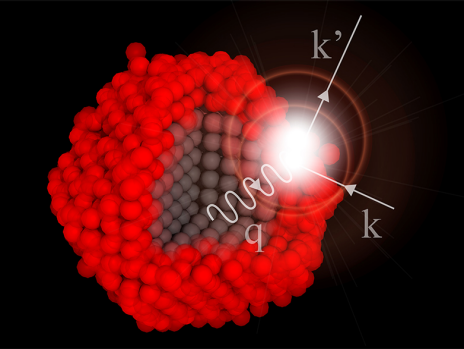
A September 20, 2021 news item on phys.org announces research investigating the heating of electronics at the nanoscale,

A team of physicists at CU Boulder [University of Colorado at Boulder] has solved the mystery behind a perplexing phenomenon in the nano realm: why some ultra-small heat sources cool down faster if you pack them closer together. The findings, published today in the journal Proceedings of the National Academy of Sciences (PNAS), could one day help the tech industry design faster electronic devices that overheat less.

A September 20, 2021 UC Boulder news release (also on EurekAlert) by Daniel Strain, which originated the news item, delves further into the topic of heat and electronics (Note: Links have been removed),

“Often, heat is a challenging consideration in designing electronics. You build a device then discover that it’s heating up faster than desired,” said study co-author Joshua Knobloch, postdoctoral research associate at JILA, a joint research institute between CU Boulder and the National Institute of Standards and Technology (NIST). “Our goal is to understand the fundamental physics involved so we can engineer future devices to efficiently manage the flow of heat.”

The research began with an unexplained observation: In 2015, researchers led by physicists Margaret Murnane and Henry Kapteyn at JILA were experimenting with bars of metal that were many times thinner than the width of a human hair on a silicon base. When they heated those bars up with a laser, something strange occurred.

“They behaved very counterintuitively,” Knobloch said. “These nano-scale heat sources do not usually dissipate heat efficiently. But if you pack them close together, they cool down much more quickly.”

Now, the researchers know why it happens.

In the new study, they used computer-based simulations to track the passage of heat from their nano-sized bars. They discovered that when they placed the heat sources close together, the vibrations of energy they produced began to bounce off each other, scattering heat away and cooling the bars down.

The group’s results highlight a major challenge in designing the next generation of tiny devices, such as microprocessors or quantum computer chips: When you shrink down to very small scales, heat does not always behave the way you think it should.

Atom by atom

The transmission of heat in devices matters, the researchers added. Even minute defects in the design of electronics like computer chips can allow temperature to build up, adding wear and tear to a device. As tech companies strive to produce smaller and smaller electronics, they’ll need to pay more attention than ever before to phonons—vibrations of atoms that carry heat in solids.

“Heat flow involves very complex processes, making it hard to control,” Knobloch said. “But if we can understand how phonons behave on the small scale, then we can tailor their transport, allowing us to build more efficient devices.”

To do just that, Murnane and Kapteyn and their team of experimental physicists joined forces with a group of theorists led by Mahmoud Hussein, professor in the Ann and H.J. Smead Department of Aerospace Engineering Sciences. His group specializes in simulating, or modeling, the motion of phonons.

“At the atomic scale, the very nature of heat transfer emerges in a new light,” said Hussein who also has a courtesy appointment in the Department of Physics.

The researchers, essentially, recreated their experiment from several years before, but this time, entirely on a computer. They modeled a series of silicon bars, laid side by side like the slats in a train track and heated them up.

The simulations were so detailed, Knobloch said, that the team could follow the behavior of each and every atom in the model—millions of them in all—from start to finish.

“We were really pushing the limits of memory of the Summit Supercomputer at CU Boulder,” he said.

Directing heat

The technique paid off. The researchers found, for example, that when they spaced their silicon bars far enough apart, heat tended to escape away from those materials in a predictable way. The energy leaked from the bars and into the material below them, dissipating in every direction.

When the bars got closer together, however, something else happened. As the heat from those sources scattered, it effectively forced that energy to flow more intensely away from the sources—like a crowd of people in a stadium jostling against each other and eventually leaping out of the exit. The team denoted this phenomenon “directional thermal channeling.”

“This phenomenon increases the transport of heat down into the substrate and away from the heat sources,” Knobloch said.

The researchers suspect that engineers could one day tap into this unusual behavior to gain a better handle on how heat flows in small electronics—directing that energy along a desired path, instead of letting it run wild and free.

For now, the researchers see the latest study as what scientists from different disciplines can do when they work together.

“This project was such an exciting collaboration between science and engineering—where advanced computational analysis methods developed by Mahmoud’s group were critical for understanding new materials behavior uncovered earlier by our group using new extreme ultraviolet quantum light sources,” said Murnane, also a professor of physics.

Here’s a link to and a citation for the paper,

Directional thermal channeling: A phenomenon triggered by tight packing of heat sources by Hossein Honarvar, Joshua L. Knobloch, Travis D. Frazer, Begoña Abad, Brendan McBennett, Mahmoud I. Hussein, Henry C. Kapteyn, Margaret M. Murnane, and Jorge N. Hernandez-Charpak. PNAS October 5, 2021 118 (40) e2109056118; DOI: https://doi.org/10.1073/pnas.2109056118

This paper is behind a paywall.

Understanding the fundamental limits of graphene electronics by way of a new quantum phenomenon

A July 26, 2019 news item on Nanowerk takes us into the world of quantum physics and graphene (Note: Links have been removed),

A team of researchers from the Universities of Manchester, Nottingham and Loughborough have discovered quantum phenomena that helps to understand the fundamental limits of graphene electronics.

As published in Nature Communications (“Strong magnetophonon oscillations in extra-large graphene”), the work describes how electrons in a single atomically-thin sheet of graphene scatter off the vibrating carbon atoms which make up the hexagonal crystal lattice.

By applying a magnetic field perpendicular to the plane of graphene, the current-carrying electrons are forced to move in closed circular “cyclotron” orbits. In pure graphene, the only way in which an electron can escape from this orbit is by bouncing off a “phonon” in a scattering event. These phonons are particle-like bundles of energy and momentum and are the “quanta” of the sound waves associated with the vibrating carbon atom. The phonons are generated in increasing numbers when the graphene crystal is warmed up from very low temperatures.

By passing a small electrical current through the graphene sheet, the team were able to measure precisely the amount of energy and momentum that is transferred between an electron and a phonon during a scattering event.

A July 26, 2019 University of Manchester press release, which originated the news item, provides additional technical details,

Their experiment revealed that two types of phonon scatter the electrons: transverse acoustic (TA) phonons in which the carbon atoms vibrate perpendicular to the direction of phonon propagation and wave motion (somewhat analogous to surface waves on water) and longitudinal acoustic (LA) phonons in which the carbon atoms vibrate back and forth along the direction of the phonon and the wave motion; (this motion is somewhat analogous to the motion of sound waves through air).

The measurements provide a very accurate measure of the speed of both types of phonons, a measurement which is otherwise difficult to make for the case of a single atomic layer. An important outcome of the experiments is the discovery that TA phonon scattering dominates over LA phonon scattering.

The observed phenomena, commonly referred to as “magnetophonon oscillations”, was measured in many semiconductors years before the discovery of graphene. It is one of the oldest quantum transport phenomena that has been known for more than fifty years, predating the quantum Hall effect. Whereas graphene possesses a number of novel, exotic electronic properties, this rather fundamental phenomenon has remained hidden.

Laurence Eaves & Roshan Krishna Kumar, co-authors of the work said: “We were pleasantly surprised to find such prominent magnetophonon oscillations appearing in graphene. We were also puzzled why people had not seen them before, considering the extensive amount of literature on quantum transport in graphene.”

Their appearance requires two key ingredients. First, the team had to fabricate high quality graphene transistors with large areas at the National Graphene Institute. If the device dimensions are smaller than a few micrometres the phenomena could not be observed.

Piranavan Kumaravadivel from The University of Manchester, lead author of the paper said: “At the beginning of quantum transport experiments, people used to study macroscopic, millimetre sized crystals. In most of the work on quantum transport on graphene, the studied devices are typically only a few micrometres in size. It seems that making larger graphene devices is not only important for applications but now also for fundamental studies.”

The second ingredient is temperature. Most graphene quantum transport experiments are performed at ultra-cold temperatures in-order to slow down the vibrating carbon atoms and “freeze-out” the phonons that usually break quantum coherence. Therefore, the graphene is warmed up as the phonons need to be active to cause the effect.

Mark Greenaway, from Loughborough University, who worked on the quantum theory of this effect said: “This result is extremely exciting – it opens a new route to probe the properties of phonons in two-dimensional crystals and their heterostructures. This will allow us to better understand electron-phonon interactions in these promising materials, understanding which is vital to develop them for use in new devices and applications.”

Here’s a link to and a citation for the paper,

Strong magnetophonon oscillations in extra-large graphene by P. Kumaravadivel, M. T. Greenaway, D. Perello, A. Berdyugin, J. Birkbeck, J. Wengraf, S. Liu, J. H. Edgar, A. K. Geim, L. Eaves & R. Krishna Kumar. ature Communicationsvolume 10, Article number: 3334 (2019) DOI: https://doi.org/10.1038/s41467-019-11379-3 Published 26 July 2019

This paper is open access.

Using sound to transfer quantum information

It seems sound is becoming more prominent as a means of science data communication (data sonification) and in this upcoming case, data transfer. From a June 5, 2018 news item on ScienceDaily,

Quantum physics is on the brink of a technological breakthrough: new types of sensors, secure data transmission methods and maybe even computers could be made possible thanks to quantum technologies. However, the main obstacle here is finding the right way to couple and precisely control a sufficient number of quantum systems (for example, individual atoms).

A team of researchers from TU Wien and Harvard University has found a new way to transfer the necessary quantum information. They propose using tiny mechanical vibrations. The atoms are coupled with each other by ‘phonons’ — the smallest quantum mechanical units of vibrations or sound waves.

A June 5, 2018 Technical University of Vienna (TU Wien) press release, which originated the news item, explains the work in greater detail,

“We are testing tiny diamonds with built-in silicon atoms – these quantum systems are particularly promising,” says Professor Peter Rabl from TU Wien. “Normally, diamonds are made exclusively of carbon, but adding silicon atoms in certain places creates defects in the crystal lattice where quantum information can be stored.” These microscopic flaws in the crystal lattice can be used like a tiny switch that can be switched between a state of higher energy and a state of lower energy using microwaves.

Together with a team from Harvard University, Peter Rabl’s research group has developed a new idea to achieve the targeted coupling of these quantum memories within the diamond. One by one they can be built into a tiny diamond rod measuring only a few micrometres in length, like individual pearls on a necklace. Just like a tuning fork, this rod can then be made to vibrate – however, these vibrations are so small that they can only be described using quantum theory. It is through these vibrations that the silicon atoms can form a quantum-mechanical link to each other.

“Light is made from photons, the quantum of light. In the same way, mechanical vibrations or sound waves can also be described in a quantum-mechanical manner. They are comprised of phonons – the smallest possible units of mechanical vibration,” explains Peter Rabl. As the research team has now been able to show using simulation calculations, any number of these quantum memories can be linked together in the diamond rod thanks to these phonons. The individual silicon atoms are “switched on and off” using microwaves. During this process, they emit or absorb phonons. This creates a quantum entanglement of different silicon defects, thus allowing quantum information to be transferred.

The road to a scalable quantum network
Until now it was not clear whether something like this was even possible: “Usually you would expect the phonons to be absorbed somewhere, or to come into contact with the environment and thus lose their quantum mechanical properties,” says Peter Rabl. “Phonons are the enemy of quantum information, so to speak. But with our calculations, we were able to show that, when controlled appropriately using microwaves, the phonons are in fact useable for technical applications.”

The main advantage of this new technology lies in its scalability: “There are many ideas for quantum systems that, in principle, can be used for technological applications. The biggest problem is that it is very difficult to connect enough of them to be able to carry out complicated computing operations,” says Peter Rabl. The new strategy of using phonons for this purpose could pave the way to a scalable quantum technology.

Here’s a link to and a citation for the paper,

Phonon Networks with Silicon-Vacancy Centers in Diamond Waveguides by M.-A. Lemonde, S. Meesala, A. Sipahigil, M. J. A. Schuetz, M. D. Lukin, M. Loncar, and P. Rabl. Phys. Rev. Lett. 120 (21), 213603 DOI:https://doi.org/10.1103/PhysRevLett.120.213603 Published 25 May 2018

This paper is behind a paywall.

Phenomen: a future and emerging information technology project

A Sept. 19, 2016 news item on Nanowerk describes a new research project incorporating photonics, phononics, and radio frequency signal processing,

HENOMEN is a ground breaking project designed to harness the potential of combined phononics, photonics and radio-frequency (RF) electronic signals to lay the foundations of a new information technology. This new Project, funded though the highly competitive H2020 [the European Union’s Horizon 2020 science funding programme] FET [Future and Emerging Technologies]-Open call, joins the efforts of three leading research institutes, three internationally recognised universities and a high-tech SME. The Consortium members kick-offed the project with a meeting on Friday September 16, 2016, at the Catalan Institute of Nanoscience and Nanotechnology (ICN2), coordinated by ICREA Research Prof Dr Clivia M. Sotomayor-Torres, of the ICN2’ Phononic and Photonic Nanostructures (P2N) Group.

A Sept. 16, 2016 ICN2 press release, which originated the news item, provides more detail,

Most information is currently transported by electrical charge (electrons) and by light (photons). Phonons are the quanta of lattice vibrations with frequencies covering a wide range up to tens of THz and provide coupling to the surrounding environment. In PHENOMEN the core of the research will be focused on phonon-based signal processing to enable on-chip synchronisation and transfer information carried between optical channels by phonons.

This ambitious prospect could serve as a future scalable platform for, e.g., hybrid information processing with phonons. To achieve it, PHENOMEN proposes to build the first practical optically-driven phonon sources and detectors including the engineering of phonon lasers to deliver coherent phonons to the rest of the chip pumped by a continuous wave optical source. It brings together interdisciplinary scientific and technology oriented partners in an early-stage research towards the development of a radically new technology.

The experimental implementation of phonons as information carriers in a chip is completely novel and of a clear foundational character. It deals with interaction and manipulation of fundamental particles and their intrinsic dual wave-particle character. Thus, it can only be possible with the participation of an interdisciplinary consortium which will create knowledge in a synergetic fashion and add value in the form of new theoretical tools,  develop novel methods to manipulate coherent phonons with light and build all-optical phononic circuits enabled by optomechanics.

The H2020 FET-Open call “Novel ideas for radically new technologies” aims to support the early stages of joint science and technology research for radically new future technological possibilities. The call is entirely non-prescriptive with regards to the nature or purpose of the technologies that are envisaged and thus targets mainly the unexpected. PHENOMEN is one of the 13 funded Research & Innovation Actions and went through a selection process with a success rate (1.4%) ten times smaller than that for an ERC grant. The retained proposals are expected to foster international collaboration in a multitude of disciplines such as robotics, nanotechnology, neuroscience, information science, biology, artificial intelligence or chemistry.

The Consortium

The PHENOMEN Consortium is made up by:

  • 3 leading research institutes:
  • 3 universities with an internationally recognised track-record in their respective areas of expertise:
  • 1 industrial partner:

How vibrations affect nanoscale materials

A March 9, 2016 news item on ScienceDaily announces work concerning atomic vibrations,

All materials are made up of atoms, which vibrate. These vibrations, or ‘phonons’, are responsible, for example, for how electric charge and heat is transported in materials. Vibrations of metals, semiconductors, and insulators in are well studied; however, now materials are being nanosized to bring better performance to applications such as displays, sensors, batteries, and catalytic membranes. What happens to vibrations when a material is nanosized has until now not been understood.

A March 9, 2016 ETH Zurich press release (also on EurekAlert), which originated the news item, describes the world of vibration at the nanoscale and the potential impact this new information could have,

Soft Surfaces Vibrate Strongly

In a recent publication in Nature, ETH Professor Vanessa Wood and her colleagues explain what happens to atomic vibrations when materials are nanosized and how this knowledge can be used to systematically engineer nanomaterials for different applications.

The paper shows that when materials are made smaller than about 10 to 20 nanometers – that is, 5,000 times thinner than a human air – the vibrations of the outermost atomic layers on surface of the nanoparticle are large and play an important role in how this material behaves.

“For some applications, like catalysis, thermoelectrics, or superconductivity, these large vibrations may be good, but for other applications like LEDs or solar cells, these vibrations are undesirable,” explains Wood.

Indeed, the paper explains why nanoparticle-based solar cells have until now not met their full promise.  The researchers showed using both experiment and theory that surface vibrations interact with electrons to reduce the photocurrent in solar cells.

“Now that we have proven that surface vibrations are important, we can systematically design materials to suppress or enhance these vibrations,” say Wood.

Improving Solar Cells

Wood’s research group has worked for a long time on a particular type of nanomaterial – colloidal nanocrystals – semiconductors with a diameter of 2 to 10 nanometers.  These materials are interesting because their optical and electrical properties are dependent on their size, which can be easily changed during their synthesis.

These materials are now used commercially as red- and green-light emitters in LED-based TVs and are being explored as possible materials for low cost, solution-processed solar cells.  Researchers have noticed that placing certain atoms around the surface of the nanocrystal can improve the performance of solar cells. The reason why this worked had not been understood.  The work published in the Nature paper now gives the answer:  a hard shell of atoms can suppress the vibrations and their interaction with electrons.  This means a higher photocurrent and a higher efficiency solar cell.

Big Science to Study the Nanoscale

Experiments were conducted in Professor Wood’s labs at ETH Zurich and at the Swiss Spallation Neutron Source at the Paul Scherrer Institute. By observing how neutrons scatter off atoms in a material, it is possible to quantify how atoms in a material vibrate. To understand the neutron measurements, simulations of the atomic vibrations were run at the Swiss National Supercomputing Center (CSCS) in Lugano. Wood says, “without access to these large facilities, this work would not have been possible. We are incredibly fortunate here in Switzerland to have these world class facilities.”

The researchers have made available an image illustrating their work,

Vibrations of atoms in materials, the "phonons", are responsible for how electric charge and heat is transported in materials (Graphics: Deniz Bozyigit / ETH Zurich)

Vibrations of atoms in materials, the “phonons”, are responsible for how electric charge and heat is transported in materials (Graphics: Deniz Bozyigit / ETH Zurich)

Here’s a link to and a citation for the paper,

Soft surfaces of nanomaterials enable strong phonon interactions by Deniz Bozyigit, Nuri Yazdani, Maksym Yarema, Olesya Yarema, Weyde Matteo Mario Lin, Sebastian Volk, Kantawong Vuttivorakulchai, Mathieu Luisier, Fanni Juranyi, & Vanessa Wood. Nature (2016)  doi:10.1038/nature16977 Published online 09 March 2016

This paper is behind a paywall.

Superposition in biological processes

Applying the concept of superposition to photosynthesis and olfaction is not the first thought that would have occurred to me on stumbling across the European Union’s PAPETS project (Phonon-Assisted Processes for Energy Transfer and Sensing). Thankfully, a July 9, 2015 news item on Nanowerk sets the record straight (Note: A link has been removed),

Quantum physics is helping researchers to better understand photosynthesis and olfaction.

Can something be for instance in two different places at the same time? According to quantum physics, it can. More precisely, in line with the principle of ‘superposition’, a particle can be described as being in two different states simultaneously.

While it may sound like voodoo to the non-expert, superposition is based on solid science. Researchers in the PAPETS project are exploring this and other phenomena on the frontier between biology and quantum physics. Their goal is to determine the role of vibrational dynamics in photosynthesis and olfaction.

A July 7, 2015 research news article on the CORDIS website, which originated the news item, further explains (Note: A link has been removed),

Quantum effects in a biological system, namely in a photosynthetic complex, were first observed by Greg Engel and collaborators in 2007, in the USA. These effects were reproduced in different laboratories at a temperature of around -193 degrees Celsius and subsequently at ambient temperature.

‘What’s surprising and exciting is that these quantum effects have been observed in biological complexes, which are large, wet and noisy systems,’ says PAPETS project coordinator, Dr. Yasser Omar, researcher at Instituto de Telecomunicações and professor at Universidade de Lisboa [Portugal]. ‘Superposition is fragile and we would expect it to be destroyed by the environment.’

Superposition contributes to more efficient energy transport. An exciton, a quantum quasi-particle carrying energy, can travel faster along the photosynthetic complex due to the fact that it can exist in two states simultaneously. When it comes to a bifurcation it need not choose left or right. It can proceed down both paths simultaneously.

‘It’s like a maze,’ says Dr. Omar. ‘Only one door leads to the exit but the exciton can probe both left and right at the same time. It’s more efficient.’

Dr. Omar and his colleagues believe that a confluence of factors help superposition to be effected and maintained, namely the dynamics of the vibrating environment, whose role is precisely what the PAPETS project aims to understand and exploit.

Theory and experimentation meet

The theories being explored by PAPETS are also tested in experiments to validate them and gain further insights. To study quantum transport in photosynthesis, for example, researchers shoot fast laser pulses into biological systems. They then observe interference along the transport network, a signature of wavelike phenomena.

‘It’s like dropping stones into a lake,’ explains Dr. Omar. ‘You can then see whether the waves that are generated grow bigger or cancel each other when they meet.’

Applications: more efficient solar cells and odour detection

While PAPETS is essentially an exploratory project, it is generating insights that could have practical applications. PAPETS’ researchers are getting a more fundamental understanding of how photosynthesis works and this could result in the design of much more efficient solar cells.

Olfaction, the capacity to recognise and distinguish different odours, is another promising area. Experiments focus on the behaviour of Drosophila flies. So far, researchers suspect that the tunnelling of electrons associated to the internal vibrations of a molecule may be a signature of odour. Dr. Omar likens this tunnelling to a ping-pong ball resting in a bowl that goes through the side of the bowl to appear outside it.

This work could have applications in the food, water, cosmetics or drugs industries. Better artificial odour sensing could be used to detect impurities or pollution, for example.

‘Unlike seeing, hearing or touching, the sense of smell is difficult to reproduce artificially with high efficacy,’ says Dr. Omar.

The PAPETS project, involving 7 partners, runs from September 2014 to August 2016 and has a budgeted EU contribution funding of EUR 1.8 million.

You can find out more about PAPETS here. In the meantime, I found the other partners in the project (in addition to Portugal), from the PAPETS Partners webpage (Note: Links have been removed),

– Controlled Quantum Dynamics Group, Universität Ulm (UULM), Germany. PI: Martin Plenio and Susana Huelga.
– Biophysics Research Group, Vrije Universiteit Amsterdam (VUA), Netherlands. PI: Rienk van Grondelle and Roberta Croce.
– Department of Chemical Sciences, Università degli Studi di Padova (UNIPD), Italy. PI: Elisabetta Collini.
– Biomedical Sciences Research Centre “Alexander Fleming” (FLEMING), Athens, Greece. PI: Luca Turin and Efthimios M. Skoulakis.
– Biological Physics and Complex Systems Group, Centre National de la Recherche Scientifique (CNRS), Orléans, France. PI: Francesco Piazza.
– Quantum Physics of Biomolecular Processes, University College London (UCL), UK. PI: Alexandra Olaya-Castro.

Crowd computing for improved nanotechnology-enabled water filtration

This research is the product of a China/Israel/Switzerland collaboration on water filtration with involvement from the UK and Australia. Here’s some general information about the importance of water and about the collaboration in a July 5, 2015 news item on Nanowerk (Note: A link has been removed),

Nearly 800 million people worldwide don’t have access to safe drinking water, and some 2.5 billion people live in precariously unsanitary conditions, according to the Centers for Disease Control and Prevention. Together, unsafe drinking water and the inadequate supply of water for hygiene purposes contribute to almost 90% of all deaths from diarrheal diseases — and effective water sanitation interventions are still challenging scientists and engineers.

A new study published in Nature Nanotechnology (“Water transport inside carbon nanotubes mediated by phonon-induced oscillating friction”) proposes a novel nanotechnology-based strategy to improve water filtration. The research project involves the minute vibrations of carbon nanotubes called “phonons,” which greatly enhance the diffusion of water through sanitation filters. The project was the joint effort of a Tsinghua University-Tel Aviv University research team and was led by Prof. Quanshui Zheng of the Tsinghua Center for Nano and Micro Mechanics and Prof. Michael Urbakh of the TAU School of Chemistry, both of the TAU-Tsinghua XIN Center, in collaboration with Prof. Francois Grey of the University of Geneva.

A July 5, 2015 American Friends of Tel Aviv University news release (also on EurekAlert), which originated the news item, provides more details about the work,

“We’ve discovered that very small vibrations help materials, whether wet or dry, slide more smoothly past each other,” said Prof. Urbakh. “Through phonon oscillations — vibrations of water-carrying nanotubes — water transport can be enhanced, and sanitation and desalination improved. Water filtration systems require a lot of energy due to friction at the nano-level. With these oscillations, however, we witnessed three times the efficiency of water transport, and, of course, a great deal of energy saved.”

The research team managed to demonstrate how, under the right conditions, such vibrations produce a 300% improvement in the rate of water diffusion by using computers to simulate the flow of water molecules flowing through nanotubes. The results have important implications for desalination processes and energy conservation, e.g. improving the energy efficiency for desalination using reverse osmosis membranes with pores at the nanoscale level, or energy conservation, e.g. membranes with boron nitride nanotubes.

Crowdsourcing the solution

The project, initiated by IBM’s World Community Grid, was an experiment in crowdsourced computing — carried out by over 150,000 volunteers who contributed their own computing power to the research.

“Our project won the privilege of using IBM’s world community grid, an open platform of users from all around the world, to run our program and obtain precise results,” said Prof. Urbakh. “This was the first project of this kind in Israel, and we could never have managed with just four students in the lab. We would have required the equivalent of nearly 40,000 years of processing power on a single computer. Instead we had the benefit of some 150,000 computing volunteers from all around the world, who downloaded and ran the project on their laptops and desktop computers.

“Crowdsourced computing is playing an increasingly major role in scientific breakthroughs,” Prof. Urbakh continued. “As our research shows, the range of questions that can benefit from public participation is growing all the time.”

The computer simulations were designed by Ming Ma, who graduated from Tsinghua University and is doing his postdoctoral research in Prof. Urbakh’s group at TAU. Ming catalyzed the international collaboration. “The students from Tsinghua are remarkable. The project represents the very positive cooperation between the two universities, which is taking place at XIN and because of XIN,” said Prof. Urbakh.

Other partners in this international project include researchers at the London Centre for Nanotechnology of University College London; the University of Geneva; the University of Sydney and Monash University in Australia; and the Xi’an Jiaotong University in China. The researchers are currently in discussions with companies interested in harnessing the oscillation knowhow for various commercial projects.


Here’s a link to and a citation for the paper,

Water transport inside carbon nanotubes mediated by phonon-induced oscillating friction by Ming Ma, François Grey, Luming Shen, Michael Urbakh, Shuai Wu,    Jefferson Zhe Liu, Yilun Liu, & Quanshui Zheng. Nature Nanotechnology (2015) doi:10.1038/nnano.2015.134 Published online 06 July 2015

This paper is behind a paywall.

Final comment, I find it surprising that they used labour and computing power from 150,000 volunteers and didn’t offer open access to the paper. Perhaps the volunteers got their own copy? I certainly hope so.

Whispering about optomechanics and microfluidics

Whispering galleries are magical, wonderful places which Gaurav Bahl evokes in his June 7, 2013 University of Illinois news release on EurekAlert,

Ever been to a whispering gallery—a quiet, circular space underneath an old cathedral dome that captures and amplifies sounds as quiet as a whisper? Researchers at the University of Illinois at Urbana-Champaign are applying similar principles in the development optomechanical sensors that will help unlock vibrational secrets of chemical and biological samples at the nanoscale.

In glass microcavities that function as optical whispering galleries, according to Bahl, these miniscule optical forces can be enhanced by many orders-of-magnitude, which enables ‘conversations’ between light (photons) and vibration (phonons). These devices are of interest to condensed matter physics as the strong phonon-photon coupling enables experiments targeting quantum information storage (i.e. qubits), quantum-mechanical ground state (i.e. optomechanical cooling), and ultra-sensitive force measurements past the standard quantum limit.

Researchers developed a hollow optomechanical device made of fused silica glass, through which fluids and gases could flow. Employing a unique optomechanical interaction called Brillouin Optomechanics (described previously in Bahl et al, Nature Communications 2:403, 2011; Bahl et al, Nature Physics, vol.8, no.3, 2012), the researchers achieved the optical excitation of mechanical whispering-gallery modes at a phenomenal range of frequencies spanning from 2 MHz to 11,000 MHz.

“These mechanical vibrations can, in turn, ‘talk’ to liquids within the hollow device and provide optical readout of the mechanical properties,” said Bahl, who is first author of the paper, “Brillouin cavity optomechanics with microfluidic devices,” published this week in Nature Communications.

By confining various liquids inside a hollow microfluidic optomechanical (μFOM) resonator, researchers built the first-ever bridge between optomechanics and microfluidics.

If I read the news release correctly, there will be biomedical applications for this work,

Potential uses for this technology include optomechanical biosensors that can measure various optical and mechanical properties of a single cell, ultra-high-frequency analysis of fluids, and the optical control of fluid flow.

Here’s a link to and citation for the research paper,

Brillouin cavity optomechanics with microfluidic devices by Gaurav Bahl, Kyu Hyun Kim, Wonsuk Lee, Jing Liu, Xudong Fan,  & Tal Carmon  Nature Communications 4, Article number: 1994 doi:10.1038/ncomms2994 Published: 07 June 2013

This paper is behind a paywall.

BTW, there is a sound tourism website that includes this page on the whispering gallery in St. Paul’s Cathedral (London, England).