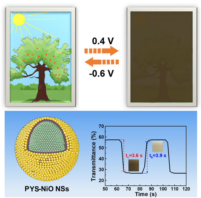
Tag Archives: Tsinghua University

Ultrafast neuromorphic (brainlike) computing at room temperature made possible by utilizing polariton nonlinearities

A June 6, 2025 news item on Nanowerk describes research into the development of ultrafast neuromorphic (brainlike) computing, Note: A link has been removed,

Neuromorphic computing, inspired by the human brain, is considered as the next-generation paradigm for artificial intelligence (AI), offering dramatically increased speed and lower energy consumption. While software-based artificial neural networks (ANNs) have made remarkable strides, unlocking their full potential calls for physical platforms that combine ultrafast operation, high computational density, energy efficiency, and scalability.

Among various physical systems, microcavity exciton polaritons have attracted attention for neuromorphic computing due to their ultrafast dynamics, strong nonlinearities, and light-based architecture, which naturally align with the requirements of brain-inspired computation. However, their practical use has been hampered by the need for cryogenic operation and intricate fabrication processes.

In a new paper published in eLight (“Ultrafast neuromorphic computing driven by polariton nonlinearities”), a team of scientists led by Professor Qihua Xiong from Tsinghua University and Beijing Academy of Quantum Information Sciences report a demonstration of neuromorphic computing utilizing perovskite microcavity exciton polaritons operating at room temperature. Their novel system achieves high-speed digit recognition with 92% accuracy using only single-step training and opens new opportunities for scalable, light-driven neural hardware.

A June 4, 2025 Light Publishing Center, Changchun Institute of Optics, Fine Mechanics And Physics, CAS (Chinese Academy of Sciences) press release on EurekAlert, which originated the news item, provides more technical details,

The core of their system is a planar FAPbBr3 perovskite microcavity which supports exciton-polariton condensation under non-resonant optical pumping. Input images from the MNIST dataset are optically encoded by a spatial light modulator (SLM) and projected onto the microcavity as spatially structured excitation beams. The resulting polariton emission patterns serve as the output of the ANN, which is then linearly processed using ridge regression. Remarkably, this scheme requires no predefined network structure—only the physical response of the polariton system—and achieves competitive accuracy using a lightweight training set of 900 images.

“Unlike conventional approaches that rely on prefabricated structures or predefined network nodes, our method employs a fully connected spatial mapping, utilizing the entire perovskite sample area without additional structural constraints,” the corresponding author Qihua Xiong replied. This not only improves the system’s scalability but also simplifies experimental realization.

What makes this system stand out is the intrinsic nonlinear and dynamical response of the polaritons. The researchers show that below the condensation threshold, the system behaves nearly linearly, while near and above threshold, nonlinearities emerge sharply, enhancing pattern discrimination. Moreover, by applying ultrafast Kerr-gated time-resolved photoluminescence, the team probes the temporal evolution of polariton responses. They find that polariton dynamics unfold on the picosecond scale and exhibit time-dependent nonlinear mappings, which significantly broaden the system’s capacity for processing complex and temporally varying inputs.

The researchers conclude that “perovskite microcavity exciton polaritons offer ultrafast processing speeds on the picosecond timescale and exhibit exceptionally strong nonlinear interactions, significantly surpassing those in traditional photonic systems.” These attributes make them powerful candidates for future physical neural networks capable of real-time, energy-efficient AI.

This work highlights the growing role of halide perovskites in next-generation photonic computing and marks an important step toward developing all-optical neuromorphic hardware—free from the energy and speed limitations of traditional electronics.

Here’s a link to and a citation for the paper,

Ultrafast neuromorphic computing driven by polariton nonlinearities by Yusong Gan, Ying Shi, Sanjib Ghosh, Haiyun Liu, Huawen Xu & Qihua Xiong. eLight volume 5, Article number: 9 (2025) DOI: https://doi.org/10.1186/s43593-025-00087-9 Published: 02 June 2025

This paper is open access.

Memristor-based brain-computer interfaces (BCIs)

Brief digression: For anyone unfamiliar with memristors, they are, for want of better terms, devices or elements that have memory in addition to their resistive properties. (For more see: R Jagan Mohan Rao’s undated article ‘What is a Memristor? Principle, Advantages, Applications” on InsstrumentalTools.com)

A March 27,2025 news item on ScienceDaily announces a memristor-enhanced brain-computer interface (BCI),

Summary: Researchers have conducted groundbreaking research on memristor-based brain-computer interfaces (BCIs). This research presents an innovative approach for implementing energy-efficient adaptive neuromorphic decoders in BCIs that can effectively co-evolve [emphasis mine] with changing brain signals.

So, the decoder in the BCI will ‘co-evolve’ with your brain? hmmm Also, where is this ‘memristor chip’? The video demo (https://assets-eu.researchsquare.com/files/rs-3966063/v1/7a84dc7037b11bad96ae0378.mp4) shows a volunteer wearing cap attached by cable to an intermediary device (an enlarged chip with a brain on it?) which is in turn attached to a screen. I believe some artistic licence has been taken with regard to the brain on the chip..

Caption: Researchers propose an adaptive neuromorphic decoder supporting brain-machine co-evolution. Credit: The University of Hong Kong

A March 25, 2025 University of Hong Kong (HKU) press release (also on EurekAlert but published on March 26, 2025), which originated the news item, explains more about memristors, BCIs, and co-evolution,

Professor Ngai Wong and Dr Zhengwu Liu from the Department of Electrical and Electronic Engineering at the Faculty of Engineering at the University of Hong Kong (HKU), in collaboration with research teams at Tsinghua University and Tianjin University, have conducted groundbreaking research on memristor-based brain-computer interfaces (BCIs). Published in Nature Electronics, this research presents an innovative approach for implementing energy-efficient adaptive neuromorphic decoders in BCIs that can effectively co-evolve with changing brain signals.

A brain-computer interface (BCI) is a computer-based system that creates a direct communication pathway between the brain and external devices, such as computers, allowing individuals to control these devices or applications purely through brain activity, bypassing the need for traditional muscle movements or the nervous system. This technology holds immense potential across a wide range of fields, from assistive technologies to neurological rehabilitation. However, traditional BCIs still face challenges.

“The brain is a complex dynamic system with signals that constantly evolve and fluctuate. This poses significant challenges for BCIs to maintain stable performance over time,” said Professor Wong and Dr Liu. “Additionally, as brain-machine links grow in complexity, traditional computing architectures struggle with real-time processing demands.”

The collaborative research addressed these challenges by developing a 128K-cell memristor chip that serves as an adaptive brain signal decoder. The team introduced a hardware-efficient one-step memristor decoding strategy that significantly reduces computational complexity while maintaining high accuracy. Dr Liu, a Research Assistant Professor in the Department of Electrical and Electronic Engineering at HKU, contributed as a co-first author to this groundbreaking work.

In real-world testing, the system demonstrated impressive capabilities in a four-degree-of-freedom drone flight control task, achieving 85.17% decoding accuracy—equivalent to software-based methods—while consuming 1,643 times less energy and offering 216 times higher normalised speed than conventional CPU-based systems.

Most significantly, the researchers developed an interactive update framework that enables the memristor decoder and brain signals to adapt to each other naturally. This co-evolution, demonstrated in experiments involving ten participants over six-hour sessions, resulted in approximately 20% higher accuracy compared to systems without co-evolution capability.

“Our work on optimising the computational models and error mitigation techniques was crucial to ensure that the theoretical advantages of memristor technology could be realised in practical BCI applications,” explained Dr Liu. “The one-step decoding approach we developed together significantly reduces both computational complexity and hardware costs, making the technology more accessible for a wide range of practical scenarios.”

Professor Wong further emphasised, “More importantly, our interactive updating framework enables co-evolution between the memristor decoder and brain signals, addressing the long-term stability issues faced by traditional BCIs. This co-evolution mechanism allows the system to adapt to natural changes in brain signals over time, greatly enhancing decoding stability and accuracy during prolonged use.”

Building on the success of this research, the team is now expanding their work through a new collaboration with HKU Li Ka Shing Faculty of Medicine and Queen Mary Hospital to develop a multimodal large language model for epilepsy data analysis.

“This new collaboration aims to extend our work on brain signal processing to the critical area of epilepsy diagnosis and treatment,” said Professor Wong and Dr Liu. “By combining our expertise in advanced algorithms and neuromorphic computing with clinical data and expertise, we hope to develop more accurate and efficient models to assist epilepsy patients.”

The research represents a significant step forward in human-centred hybrid intelligence, which combines biological brains with neuromorphic computing systems, opening new possibilities for medical applications, rehabilitation technologies, and human-machine interaction.

The project received support from the RGC Theme-based Research Scheme (TRS) project T45-701/22-R, the STI 2030-Major Projects, the National Natural Science Foundation of China, and the XPLORER Prize.

Here’s a link to and a citation for the paper,

A memristor-based adaptive neuromorphic decoder for brain–computer interfaces by Zhengwu Liu, Jie Mei, Jianshi Tang, Minpeng Xu, Bin Gao, Kun Wang, Sanchuang Ding, Qi Liu, Qi Qin, Weize Chen, Yue Xi, Yijun Li, Peng Yao, Han Zhao, Ngai Wong, He Qian, Bo Hong, Tzyy-Ping Jung, Dong Ming & Huaqiang Wu. Nature Electronics volume 8, pages 362–372 (2025) DOI: https://doi.org/10.1038/s41928-025-01340-2 Published online: 17 February 2025 Issue Date: April 2025

This paper is behind a paywall.

Words from the press release like “… human-centred hybrid intelligence, which combines biological brains with neuromorphic computing systems …” put me in mind of cyborgs.

China’s ex-UK ambassador clashes with ‘AI godfather’ on panel at AI Action Summit in France (February 10 – 11, 2025)

The Artificial Intelligence (AI) Action Summit held from February 10 – 11, 2025 in Paris seems to have been pretty exciting, President Emanuel Macron announced a 09B euros investment in the French AI sector on February 10, 2025 (I have more in my February 13, 2025 posting [scroll down to the ‘What makes Canadian (and Greenlandic) minerals and water so important?’ subhead]). I also have this snippet, which suggests Macron is eager to provide an alternative to US domination in the field of AI, from a February 10, 2025 posting on CCGTN (China Global Television Network),

French President Emmanuel Macron announced on Sunday night [February 10, 2025] that France is set to receive a total investment of 109 billion euros (approximately $112 billion) in artificial intelligence over the coming years.

Speaking in a televised interview on public broadcaster France 2, Macron described the investment as “the equivalent for France of what the United States announced with ‘Stargate’.”

He noted that the funding will come from the United Arab Emirates, major American and Canadian investment funds [emphases mine], as well as French companies.

Prime Minister Justin Trudeau attended the AI Action Summit on Tuesday, February 11, 2025 according to a Canadian Broadcasting Corporation (CBC) news online article by Ashley Burke and Olivia Stefanovich,

Prime Minister Justin Trudeau warned U.S. Vice-President J.D. Vance that punishing tariffs on Canadian steel and aluminum will hurt his home state of Ohio, a senior Canadian official said. 

The two leaders met on the sidelines of an international summit in Paris Tuesday [February 11, 2025], as the Trump administration moves forward with its threat to impose 25 per cent tariffs on all steel and aluminum imports, including from its biggest supplier, Canada, effective March 12.

Speaking to reporters on Wednesday [February 12, 2025] as he departed from Brussels, Trudeau characterized the meeting as a brief chat that took place as the pair met.

“It was just a quick greeting exchange,” Trudeau said. “I highlighted that $2.2 billion worth of steel and aluminum exports from Canada go directly into the Ohio economy, often to go into manufacturing there.

“He nodded, and noted it, but it wasn’t a longer exchange than that.”

Vance didn’t respond to Canadian media’s questions about the tariffs while arriving at the summit on Tuesday [February 11, 2025].

Additional insight can be gained from a February 10, 2025 PBS (US Public Broadcasting Service) posting of an AP (Associated Press) article with contributions from Kelvin Chan and Angela Charlton in Paris, Ken Moritsugu in Beijing, and Aijaz Hussain in New Delhi,

JD Vance stepped onto the world stage this week for the first time as U.S. vice president, using a high-stakes AI summit in Paris and a security conference in Munich to amplify Donald Trump’s aggressive new approach to diplomacy.

The 40-year-old vice president, who was just 18 months into his tenure as a senator before joining Trump’s ticket, is expected, while in Paris, to push back on European efforts to tighten AI oversight while advocating for a more open, innovation-driven approach.

The AI summit has drawn world leaders, top tech executives, and policymakers to discuss artificial intelligence’s impact on global security, economics, and governance. High-profile attendees include Chinese Vice Premier Zhang Guoqing, signaling Beijing’s deep interest in shaping global AI standards.

Macron also called on “simplifying” rules in France and the European Union to allow AI advances, citing sectors like healthcare, mobility, energy, and “resynchronize with the rest of the world.”

“We are most of the time too slow,” he said.

The summit underscores a three-way race for AI supremacy: Europe striving to regulate and invest, China expanding access through state-backed tech giants, and the U.S. under Trump prioritizing a hands-off approach.

Vance has signaled he will use the Paris summit as a venue for candid discussions with world leaders on AI and geopolitics.

“I think there’s a lot that some of the leaders who are present at the AI summit could do to, frankly — bring the Russia-Ukraine conflict to a close, help us diplomatically there — and so we’re going to be focused on those meetings in France,” Vance told Breitbart News.

Vance is expected to meet separately Tuesday with Indian Prime Minister Narendra Modi and European Commission President Ursula von der Leyen, according to a person familiar with planning who spoke on the condition of anonymity.

Modi is co-hosting the summit with Macron in an effort to prevent the sector from becoming a U.S.-China battle.

Indian Foreign Secretary Vikram Misri stressed the need for equitable access to AI to avoid “perpetuating a digital divide that is already existing across the world.”

But the U.S.-China rivalry overshadowed broader international talks.

The U.S.-China rivalry didn’t entirely overshadow the talks. At least one Chinese former diplomat chose to make her presence felt by chastising a Canadian academic according to a February 11, 2025 article by Matthew Broersma for silicon.co.uk

A representative of China at this week’s AI Action Summit in Paris stressed the importance of collaboration on artificial intelligence, while engaging in a testy exchange with Yoshua Bengio, a Canadian academic considered one of the “Godfathers” of AI.

Fu Ying, a former Chinese government official and now an academic at Tsinghua University in Beijing, said the name of China’s official AI Development and Safety Network was intended to emphasise the importance of collaboration to manage the risks around AI.

She also said tensions between the US and China were impeding the ability to develop AI safely.

… Fu Ying, a former vice minister of foreign affairs in China and the country’s former UK ambassador, took veiled jabs at Prof Bengio, who was also a member of the panel.

Zoe Kleinman’s February 10, 2025 article for the British Broadcasting Corporation (BBC) news online website also notes the encounter,

A former Chinese official poked fun at a major international AI safety report led by “AI Godfather” professor Yoshua Bengio and co-authored by 96 global experts – in front of him.

Fu Ying, former vice minister of foreign affairs and once China’s UK ambassador, is now an academic at Tsinghua University in Beijing.

The pair were speaking at a panel discussion ahead of a two-day global AI summit starting in Paris on Monday [February 10, 2025].

The aim of the summit is to unite world leaders, tech executives, and academics to examine AI’s impact on society, governance, and the environment.

Fu Ying began by thanking Canada’s Prof Bengio for the “very, very long” document, adding that the Chinese translation stretched to around 400 pages and she hadn’t finished reading it.

She also had a dig at the title of the AI Safety Institute – of which Prof Bengio is a member.

China now has its own equivalent; but they decided to call it The AI Development and Safety Network, she said, because there are lots of institutes already but this wording emphasised the importance of collaboration.

The AI Action Summit is welcoming guests from 80 countries, with OpenAI chief executive Sam Altman, Microsoft president Brad Smith and Google chief executive Sundar Pichai among the big names in US tech attending.

Elon Musk is not on the guest list but it is currently unknown whether he will decide to join them. [As of February 13, 2025, Mr. Musk did not attend the summit, which ended February 11, 2025.]

A key focus is regulating AI in an increasingly fractured world. The summit comes weeks after a seismic industry shift as China’s DeepSeek unveiled a powerful, low-cost AI model, challenging US dominance.

The pair’s heated exchanges were a symbol of global political jostling in the powerful AI arms race, but Fu Ying also expressed regret about the negative impact of current hostilities between the US and China on the progress of AI safety.

She gave a carefully-crafted glimpse behind the curtain of China’s AI scene, describing an “explosive period” of innovation since the country first published its AI development plan in 2017, five years before ChatGPT became a viral sensation in the west.

She added that “when the pace [of development] is rapid, risky stuff occurs” but did not elaborate on what might have taken place.

“The Chinese move faster [than the west] but it’s full of problems,” she said.

Fu Ying argued that building AI tools on foundations which are open source, meaning everyone can see how they work and therefore contribute to improving them, was the most effective way to make sure the tech did not cause harm.

Most of the US tech giants do not share the tech which drives their products.

Open source offers humans “better opportunities to detect and solve problems”, she said, adding that “the lack of transparency among the giants makes people nervous”.

But Prof Bengio disagreed.

His view was that open source also left the tech wide open for criminals to misuse.

He did however concede that “from a safety point of view”, it was easier to spot issues with the viral Chinese AI assistant DeepSeek, which was built using open source architecture, than ChatGPT, whose code has not been shared by its creator OpenAI.

Fro anyone curious about Professor Bengio’s AI safety report, I have more information in a September 29, 2025 Université de Montréal (UdeM) press release,

The first international report on the safety of artificial intelligence, led by Université de Montréal computer-science professor Yoshua Bengio, was released today and promises to serve as a guide for policymakers worldwide. 

Announced in November 2023 at the AI Safety Summit at Bletchley Park, England, and inspired by the workings of the United Nations Intergovernmental Panel on Climate Change, the report consolidates leading international expertise on AI and its risks. 

Supported by the United Kingdom’s Department for Science, Innovation and Technology, Bengio, founder and scientific director of the UdeM-affiliated Mila – Quebec AI Institute, led a team of 96 international experts in drafting the report.

The experts were drawn from 30 countries, the U.N., the European Union and the OECD [Organisation for Economic Cooperation and Development]. Their report will help inform discussions next month at the AI Action Summit in Paris, France and serve as a global handbook on AI safety to help support policymakers.

Towards a common understanding

The most advanced AI systems in the world now have the ability to write increasingly sophisticated computer programs, identify cyber vulnerabilities, and perform on a par with human PhD-level experts on tests in biology, chemistry, and physics. 

In what is identified as a key development for policymakers to monitor, the AI Safety Report published today warns that AI systems are also increasingly capable of acting as AI agents, autonomously planning and acting in pursuit of a goal. 

As policymakers worldwide grapple with the rapid and unpredictable advancements in AI, the report contributes to bridging the gap by offering a scientific understanding of emerging risks to guide decision-making.  

The document sets out the first comprehensive, independent, and shared scientific understanding of advanced AI systems and their risks, highlighting how quickly the technology has evolved.  

Several areas require urgent research attention, according to the report, including how rapidly capabilities will advance, how general-purpose AI models work internally, and how they can be designed to behave reliably. 

Three distinct categories of AI risks are identified: 

  • Malicious use risks: these include cyberattacks, the creation of AI-generated child-sexual-abuse material, and even the development of biological weapons; 
  • System malfunctions: these include bias, reliability issues, and the potential loss of control over advanced general-purpose AI systems; 
  • Systemic risks: these stem from the widespread adoption of AI, include workforce disruption, privacy concerns, and environmental impacts.  

The report places particular emphasis on the urgency of increasing transparency and understanding in AI decision-making as the systems become more sophisticated and the technology continues to develop at a rapid pace. 

While there are still many challenges in mitigating the risks of general-purpose AI, the report highlights promising areas for future research and concludes that progress can be made.   

Ultimately, it emphasizes that while AI capabilities could advance at varying speeds, their development and potential risks are not a foregone conclusion. The outcomes depend on the choices that societies and governments make today and in the future. 

“The capabilities of general-purpose AI have increased rapidly in recent years and months,” said Bengio. “While this holds great potential for society, AI also presents significant risks that must be carefully managed by governments worldwide.  

“This report by independent experts aims to facilitate constructive and evidence-based discussion around these risks and serves as a common basis for policymakers around the world to understand general-purpose AI capabilities, risks and possible mitigations.” 

The report is more formally known as the International AI Safety Report 2025 and can be found on the gov.uk website.

There have been two previous AI Safety Summits that I’m aware of and you can read about them in my May 21, 2024 posting about the one in Korea and in my November 2, 2023 posting about the first summit at Bletchley Park in the UK.

You can find the Canadian Artificial Intelligence Safety Institute (or AI Safety Institute) here and my coverage of DeepSeek’s release and the panic in the US artificial intelligence and the business communities that ensued in my January 29, 2025 posting.

Better (safer, cheaper) battery invented for wearable tech

A June 5, 2024 news item on phys.org announces new research into ‘aqueous’ wearable batteries,

Researchers have developed a safer, cheaper, better performing and more flexible battery option for wearable devices. A paper describing the “recipe” for their new battery type was published in the journal Nano Research Energy on June 3 [2024].

Fitness trackers. Smart watches. Virtual-reality headsets. Even smart clothing and implants. Wearable smart devices are everywhere these days. But for greater comfort, reliability and longevity, these devices will require greater levels of flexibility and miniaturization of their energy storage mechanisms, which are often frustratingly bulky, heavy and fragile. On top of this, any improvements cannot come at the expense of safety.

As a result, in recent years, a great deal of battery research has focused on the development of “micro” flexible energy storage devices, or MFESDs. A range of different structures and electrochemical foundations have been explored, and among them, aqueous micro batteries offer many distinct advantages.

A June 5, 2024 Tsinghua University press release on EurekAlert, which originated the news item, provides more detail,

Aqueous batteries—those that use a water-based solution as an electrolyte (the medium that allows transport of ions in the battery and thus creating an electric circuit) are nothing new. They have been around since the late 19th century. However, their energy density—or the amount of energy contained in the battery per unit of volume—is too low for use in things like electric vehicles as they would take up too much space. Lithium-ion batteries are far more appropriate for such uses.

At the same time, aqueous batteries are much less flammable, and thus safer, than lithium-ion batteries. They are also much cheaper. As a result of this more robust safety and low cost, aqueous options have increasingly been explored as one of the better options for MFESDs. These are termed aqueous micro batteries, or just AMBs.

“Up till now, sadly, AMBs have not lived up to their potential,” said Ke Niu, a materials scientist with the Guangxi Key Laboratory of Optical and Electronic Materials and Devices at the Guilin University of Technology—one of the lead researchers on the team. “To be able to be used in a wearable device, they need to withstand a certain degree of real-world bending and twisting. But most of those explored so far fail in the face of such stress.”

To overcome this, any fractures or failure points in an AMB would need to be self-healing following such stress. Unfortunately, the self-healing AMBs that have been developed so far have tended to depend on metallic compounds as the carriers of charge in the battery’s electric circuit. This has the undesirable side-effect of strong reaction between the metal’s ions and the materials that the electrodes (the battery’s positive and negative electrical conductors) are made out of. This in turn reduces the battery’s reaction rate (the speed at which the electrochemical reactions at the heart of any battery take place), drastically limiting performance.

“So we started investigating the possibility of non-metallic charge carriers, as these would not suffer from the same difficulties from interaction with the electrodes,” added Junjie Shi, another leading member of the team and a researcher with the School of Physics and Center zfor Nanoscale Characterization & Devices (CNCD) at the Huazhong University of Science and Technology in Wuhan.

The research team alighted upon ammonium ions, derived from abundantly available ammonium salts, as the optimal charge carriers. They are far less corrosive than other options and have a wide electrochemical stability window.

“But ammonium ions are not the only ingredient in the recipe needed to make our batteries self-healing,” said Long Zhang, the third leading member of the research team, also at CNCD.

For that, the team incorporated the ammonium salts into a hydrogel—a polymer material that can absorb and retain a large amount of water without disturbing its structure. This gives hydrogels impressive flexibility—delivering precisely the sort of self-healing character needed. Gelatin is probably the most well-known hydrogel, although the researchers in this case opted for a polyvinyl alcohol hydrogel (PVA) for its great strength and low cost.

To optimize compatibility with the ammonium electrolyte, titanium carbide—a ‘2D’ nanomaterial with only a single layer of atoms—was chosen for the anode (the negative electrode) material for its excellent conductivity. Meanwhile manganese dioxide, already commonly used in dry cell batteries, was woven into a carbon nanotube matrix (again to improve conductivity) for the cathode (the positive electrode).

Testing of the prototype self-healing battery showed it exhibited excellent energy density, power density, cycle life, flexibility, and self-healing even after ten self-healing cycles.

The team now aims to further develop and optimise their prototype in preparation for commercial production.


About Nano Research Energy

Nano Research Energy is launched by Tsinghua University Press and exclusively available via SciOpen, aiming at being an international, open-access and interdisciplinary journal. We will publish research on cutting-edge advanced nanomaterials and nanotechnology for energy. It is dedicated to exploring various aspects of energy-related research that utilizes nanomaterials and nanotechnology, including but not limited to energy generation, conversion, storage, conservation, clean energy, etc. Nano Research Energy will publish four types of manuscripts, that is, Communications, Research Articles, Reviews, and Perspectives in an open-access form.

About SciOpen

SciOpen is a professional open access resource for discovery of scientific and technical content published by the Tsinghua University Press and its publishing partners, providing the scholarly publishing community with innovative technology and market-leading capabilities. SciOpen provides end-to-end services across manuscript submission, peer review, content hosting, analytics, and identity management and expert advice to ensure each journal’s development by offering a range of options across all functions as Journal Layout, Production Services, Editorial Services, Marketing and Promotions, Online Functionality, etc. By digitalizing the publishing process, SciOpen widens the reach, deepens the impact, and accelerates the exchange of ideas.

Here’s a link to and a citation for the paper,

A self-healing aqueous ammonium-ion micro batteries based on PVA-NH4Cl hydrogel electrolyte and MXene-integrated perylene anode by Ke Niu, Junjie Shi, Long Zhang, Yang Yue, Mengjie Wang, Qixiang Zhang, Yanan Ma, Shuyi Mo, Shaofei Li, Wenbiao Li, Li Wen, Yixin Hou, Fei Long, Yihua Gao. Nano Research Energy (2024)DOI: https://doi.org/10.26599/NRE.2024.9120127 Published: 03 June 2024

This paper is open access by means of a “Creative Commons Attribution 4.0 International License (http://creativecommons.org/licenses/by/4.0/), which permits use, distribution and reproduction in any medium, provided the original work is properly cited.”

Excellent electrochromic smart window performance with yolk-shell NiO (nitrogen oxide) nanospheres

Electrochromic windows hold great promise where energy savings are concerned. So far, it’s still just a promise but perhaps the research in this April 17, 2023 news item on phys.org will help realize it, Note: Links have been removed,

Researchers from Tsinghua University synthesized porous yolk-shell NiO nanospheres (PYS-NiO NSs) via a solvothermal and subsequent calcination process of Ni-MOF. As the large specific surface areas and hollow porous nanostructures were conducive to ionic transport, PYS-NiO NSs exhibited a fast coloring/bleaching speed (3.6/3.9 s per one coloring/bleaching cycle) and excellent cycling stability (82% of capacity retention after 3000 cycles). These superior electrochromic (EC) properties indicated that the PYS-NiO NSs was a promising candidate for high performance EC devices.

Electrochromic (EC) materials (ECMs) are defined as the materials which have reversible changes in their colors and optical properties (transmittance, reflectance, and absorption) under different external voltages. Over the past decades, ECMs show promising advantages and application prospects in many fields such as smart windows, adaptive camouflage, electronic displays, and energy storage, etc., because of their excellent optical modulation abilities.

This image doesn’t seem all that helpful (to me) in understanding the research,

Caption: Porous yolk-shell nanospheres exhibit a fast coloring/bleaching speed. Credit: Baoshun Wang, Tsinghua University

An April 17, 2023 Particuology (journal) news release on EurekAlert, which originated the news item, does provide more detail, Note: Links have been removed,

Transition metal oxides (TMOs) are one of the most important ECMs which have been widely studied. They have many advantages such as rich nanostructure design, simple synthesis process, high security, etc. Among them, nickel oxide (NiO) is an attractive anode ECM and has attracted extensive research interest due to its high optical contrast, high coloring efficiency, low cost, etc. However, NiO-based ECMs still face the challenges of long EC switching times and poor cycling life which are caused by their poor ionic/electronic diffusion kinetics and low electrical conductivity.

Metal-organic frameworks (MOFs) have attracted enormous attention, because of their high porosity and large surface areas, and could be adjusted to achieve different properties by selecting different metal ions and organic bridging ligands. Due to the porosity and long-range orderliness, MOFs can provide fast and convenient channels for small molecules and ions to insert and extract during the transformation process. Therefore, MOFs can be used as effective templates for the preparation of hollow and porous TMOs with high ion transport efficiency, excellent specific capacitance, and electrochemical activities.

So the authors proposed a new strategy to design a kind of NiO with hollow and porous structure to obtain excellent EC performance and cyclic stability. As a proof-of-concept demonstration, the authors successfully synthesized MOFs-derived porous yolk-shell NiO nanospheres (PYS-NiO NSs) which exhibited excellent EC performance. Ni-organic framework spheres were prepared by a simple solvothermal method and then converted to PYS-NiO NSs by thermal decomposition. The PYS-NiO NSs exhibited relatively high specific surface areas and stable hollow nanostructures, which not only provided a large contact area between active sites and electrolyte ions in the EC process but also helped the NiO to accommodate large volume changes without breaking. Besides, the PYS-NiO NSs also shortened the ionic diffusion length and provided efficient channels for transferring electronics and ions. In addition, the coupling with carbon also rendered the PYS-NiO NSs with improved electronic conductivity and obtained better EC performance. The PYS-NiO NSs exhibited a fast coloring/bleaching speed (3.6/3.9 s). Besides, PYS-NiO NSs also exhibited excellent cycling stability (82% of capacity retention after 3000 cycles). These superior EC properties indicate that the PYS-NiO NSs is a promising candidate for high-performance EC devices. The as-prepared PYS-NiO NSs are believed to be a promising candidate for smart windows, displays, antiglare rearview mirrors, etc. More importantly, this work provides a new and feasible strategy for the efficient preparation of ECMs with fast response speed and high cyclic stability.

Particuology (IF=3.251) is an interdisciplinary journal that publishes frontier research articles and critical reviews on the discovery, formulation and engineering of particulate materials, processes and systems. Topics are broadly relevant to the production of materials, pharmaceuticals and food, the conversion of energy resources, and protection of the environment. For more information, please visit: https://www.journals.elsevier.com/particuology.

Here’s a link to and a citation for the paper, Note: There is an unusually long lead time between online access and print access,

Novel self-assembled porous yolk-shell NiO nanospheres with excellent electrochromic performance for smart windows by Baoshun Wang, Ya Huang, Siming Zhao, Run Li, Di Gao, Hairong Jiang, Rufan Zhang. Particuology Volume 84, January 2024, Pages 72-80 DOI: https://doi.org/10.1016/j.partic.2023.03.007 Available online: April 17, 2023

This paper is open access.

Future firefighters and wearable technology

I imagine this wearable technology would also be useful for the military too. However, the focus for these researchers from China is firefighting. (Given the situation with the Canadian wildfires in June 2023, we have 10x more than the average at this time in the season over the last 10 years, it’s good to see some work focused on safety for firefighters.) From a January 17, 2023 news item on phys.org,

Firefighting may look vastly different in the future thanks to intelligent fire suits and masks developed by multiple research institutions in China.

Researchers published results showing breathable electrodes woven into fabric used in fire suits have proven to be stable at temperatures over 520ºC. At these temperatures, the fabric is found to be essentially non-combustible with high rates of thermal protection time.

Caption: Scientists from multiple institutions address the challenges and limitations of current fire-fighting gear by introducing wearable, breathable sensors and electrodes to better serve firefighters. Credit: Nano Research, Tsinghua University Press

A January 17, 2023 Tsinghua University Press press release on EurekAlert, which originated the news item, provides more technical details,

The results show the efficacy and practicality of Janus graphene/poly(p-phenylene benzobisoxazole), or PBO, woven fabric in making firefighting “smarter” with the main goal being to manufacture products on an industrial scale that are flame-retardant but also intelligent enough to warn the firefighter of increased risks while traversing the flames.

“Conventional firefighting clothing and fire masks can ensure firemen’s safety to a certain extent,” said Wei Fan, professor at the School of Textile Science and Engineering at Xi’an Polytechnic University. “However, the fire scene often changes quickly, sometimes making firefighters trapped in the fire for failing to judge the risks in time. At this situation, firefighters also need to be rescued.”

The key here is the use of Janus graphene/PBO, woven fabrics. While not the first of its kind, the introduction of PBO fibers offers better strength and fire protection than other similar fibers, such as Kevlar. The PBO fibers are first woven into a fabric that is then irradiated using a CO2 infrared laser. From here, the fabric becomes the Janus graphene/PBO hybrid that is the focus of the study.   

The mask also utilizes a top and bottom layer of Janus graphene/PBO with a piezoelectric layer in between that acts as a way to convert mechanical pressures to electricity.

“The mask has a good smoke particle filtration effect, and the filtration efficiency of PM2.5 and PM3.0 reaches 95% and 100%, respectively. Meanwhile, the mask has good wearing comfort as its respiratory resistance (46.8 Pa) is lower than 49 Pa of commercial masks. Besides, the mask is sensitive to the speed and intensity of human breathing, which can dynamically monitor the health of the firemen” said Fan.

Flame-retardant electronics featured in these fire suits are flexible, heat resistant, quick to make and low-cost which makes scaling for industrial production a tangible achievement. This makes it more likely that the future of firefighting suits and masks will be able to effectively use this technology. Quick, effective responses can also reduce economic losses attributed to fires.

“The graphene/PBO woven fabrics-based sensors exhibit good repeatability and stability in human motion monitoring and NO2 gas detection, the main toxic gas in fires, which can be applied to firefighting suits to help firefighters effectively avoiding danger” Fan said. Being able to detect sharp increases in NO2 gas can help firefighters change course in an instant if needed and could be a lifesaving addition to firefighter gear.

Major improvements can be made in the firefighting field to better protect the firefighters by taking advantage of graphene/PBO woven and nonwoven fabrics. Widescale use of this technology can help the researchers reach their ultimate goal of reducing mortality and injury to those who risk their lives fighting fires.

Yu Luo and Yaping Miao of the School of Textile Science and Engineering at Xi’an Polytechnic University contributed equally to this work. Professor Wei Fan is the corresponding author. Yingying Zhang and Huimin Wang of the Department of Chemistry at Tsinghua University, Kai Dong of the Beijing Institute of Nanoenergy and Nanosystems at the Chinese Academy of Sciences, and Lin Hou and Yanyan Xu of Shaanxi Textile Research Institute Co., LTD, Weichun Chen and Yao Zhang of the School of Textile Science and Engineering at Xi’an Polytechnic University contributed to this research. 

This work was supported by the National Natural Science Foundation of China, Textile Vision Basic Research Program of China, Key Research and Development Program of Xianyang Science and Technology Bureau, Key Research and Development Program of Shaanxi Province, Natural Science Foundation of Shaanxi Province, and Scientific Research Project of Shaanxi Provincial Education Department.

Here are two links and a citation for the same paper,

Laser-induced Janus graphene/poly(p-phenylene benzobisoxazole) fabrics with intrinsic flame retardancy as flexible sensors and breathable electrodes for fire-fighting field by Yu Luo, Yaping Miao, Huimin Wang, Kai Dong, Lin Hou, Yanyan Xu, Weichun Chen, Yao Zhang, Yingying Zhang & Wei Fan. Nano Research (2023) DOI: https://doi.org/10.1007/s12274-023-5382-y Published12 January 2023

This link leads to a paywall.

Here’s the second link (to SciOpen)

Laser-induced Janus graphene/poly(p-phenylene benzobisoxazole) fabrics with intrinsic flame retardancy as flexible sensors and breathable electrodes for fire-fighting field. SciOpen Published January 12, 2023

This link leads to an open access journal published by Tsinghua University Press.

New chip for neuromorphic computing runs at a fraction of the energy of today’s systems

An August 17, 2022 news item on Nanowerk announces big (so to speak) claims from a team researching neuromorphic (brainlike) computer chips,

An international team of researchers has designed and built a chip that runs computations directly in memory and can run a wide variety of artificial intelligence (AI) applications–all at a fraction of the energy consumed by computing platforms for general-purpose AI computing.

The NeuRRAM neuromorphic chip brings AI a step closer to running on a broad range of edge devices, disconnected from the cloud, where they can perform sophisticated cognitive tasks anywhere and anytime without relying on a network connection to a centralized server. Applications abound in every corner of the world and every facet of our lives, and range from smart watches, to VR headsets, smart earbuds, smart sensors in factories and rovers for space exploration.

The NeuRRAM chip is not only twice as energy efficient as the state-of-the-art “compute-in-memory” chips, an innovative class of hybrid chips that runs computations in memory, it also delivers results that are just as accurate as conventional digital chips. Conventional AI platforms are a lot bulkier and typically are constrained to using large data servers operating in the cloud.

In addition, the NeuRRAM chip is highly versatile and supports many different neural network models and architectures. As a result, the chip can be used for many different applications, including image recognition and reconstruction as well as voice recognition.

..

An August 17, 2022 University of California at San Diego (UCSD) news release (also on EurekAlert), which originated the news item, provides more detail than usually found in a news release,

“The conventional wisdom is that the higher efficiency of compute-in-memory is at the cost of versatility, but our NeuRRAM chip obtains efficiency while not sacrificing versatility,” said Weier Wan, the paper’s first corresponding author and a recent Ph.D. graduate of Stanford University who worked on the chip while at UC San Diego, where he was co-advised by Gert Cauwenberghs in the Department of Bioengineering. 

The research team, co-led by bioengineers at the University of California San Diego, presents their results in the Aug. 17 [2022] issue of Nature.

Currently, AI computing is both power hungry and computationally expensive. Most AI applications on edge devices involve moving data from the devices to the cloud, where the AI processes and analyzes it. Then the results are moved back to the device. That’s because most edge devices are battery-powered and as a result only have a limited amount of power that can be dedicated to computing. 

By reducing power consumption needed for AI inference at the edge, this NeuRRAM chip could lead to more robust, smarter and accessible edge devices and smarter manufacturing. It could also lead to better data privacy as the transfer of data from devices to the cloud comes with increased security risks. 

On AI chips, moving data from memory to computing units is one major bottleneck. 

“It’s the equivalent of doing an eight-hour commute for a two-hour work day,” Wan said. 

To solve this data transfer issue, researchers used what is known as resistive random-access memory, a type of non-volatile memory that allows for computation directly within memory rather than in separate computing units. RRAM and other emerging memory technologies used as synapse arrays for neuromorphic computing were pioneered in the lab of Philip Wong, Wan’s advisor at Stanford and a main contributor to this work. Computation with RRAM chips is not necessarily new, but generally it leads to a decrease in the accuracy of the computations performed on the chip and a lack of flexibility in the chip’s architecture. 

“Compute-in-memory has been common practice in neuromorphic engineering since it was introduced more than 30 years ago,” Cauwenberghs said.  “What is new with NeuRRAM is that the extreme efficiency now goes together with great flexibility for diverse AI applications with almost no loss in accuracy over standard digital general-purpose compute platforms.”

A carefully crafted methodology was key to the work with multiple levels of “co-optimization” across the abstraction layers of hardware and software, from the design of the chip to its configuration to run various AI tasks. In addition, the team made sure to account for various constraints that span from memory device physics to circuits and network architecture. 

“This chip now provides us with a platform to address these problems across the stack from devices and circuits to algorithms,” said Siddharth Joshi, an assistant professor of computer science and engineering at the University of Notre Dame , who started working on the project as a Ph.D. student and postdoctoral researcher in Cauwenberghs lab at UC San Diego. 

Chip performance

Researchers measured the chip’s energy efficiency by a measure known as energy-delay product, or EDP. EDP combines both the amount of energy consumed for every operation and the amount of times it takes to complete the operation. By this measure, the NeuRRAM chip achieves 1.6 to 2.3 times lower EDP (lower is better) and 7 to 13 times higher computational density than state-of-the-art chips. 

Researchers ran various AI tasks on the chip. It achieved 99% accuracy on a handwritten digit recognition task; 85.7% on an image classification task; and 84.7% on a Google speech command recognition task. In addition, the chip also achieved a 70% reduction in image-reconstruction error on an image-recovery task. These results are comparable to existing digital chips that perform computation under the same bit-precision, but with drastic savings in energy. 

Researchers point out that one key contribution of the paper is that all the results featured are obtained directly on the hardware. In many previous works of compute-in-memory chips, AI benchmark results were often obtained partially by software simulation. 

Next steps include improving architectures and circuits and scaling the design to more advanced technology nodes. Researchers also plan to tackle other applications, such as spiking neural networks.

“We can do better at the device level, improve circuit design to implement additional features and address diverse applications with our dynamic NeuRRAM platform,” said Rajkumar Kubendran, an assistant professor for the University of Pittsburgh, who started work on the project while a Ph.D. student in Cauwenberghs’ research group at UC San Diego.

In addition, Wan is a founding member of a startup that works on productizing the compute-in-memory technology. “As a researcher and  an engineer, my ambition is to bring research innovations from labs into practical use,” Wan said. 

New architecture 

The key to NeuRRAM’s energy efficiency is an innovative method to sense output in memory. Conventional approaches use voltage as input and measure current as the result. But this leads to the need for more complex and more power hungry circuits. In NeuRRAM, the team engineered a neuron circuit that senses voltage and performs analog-to-digital conversion in an energy efficient manner. This voltage-mode sensing can activate all the rows and all the columns of an RRAM array in a single computing cycle, allowing higher parallelism. 

In the NeuRRAM architecture, CMOS neuron circuits are physically interleaved with RRAM weights. It differs from conventional designs where CMOS circuits are typically on the peripheral of RRAM weights.The neuron’s connections with the RRAM array can be configured to serve as either input or output of the neuron. This allows neural network inference in various data flow directions without incurring overheads in area or power consumption. This in turn makes the architecture easier to reconfigure. 

To make sure that accuracy of the AI computations can be preserved across various neural network architectures, researchers developed a set of hardware algorithm co-optimization techniques. The techniques were verified on various neural networks including convolutional neural networks, long short-term memory, and restricted Boltzmann machines. 

As a neuromorphic AI chip, NeuroRRAM performs parallel distributed processing across 48 neurosynaptic cores. To simultaneously achieve high versatility and high efficiency, NeuRRAM supports data-parallelism by mapping a layer in the neural network model onto multiple cores for parallel inference on multiple data. Also, NeuRRAM offers model-parallelism by mapping different layers of a model onto different cores and performing inference in a pipelined fashion.

An international research team

The work is the result of an international team of researchers. 

The UC San Diego team designed the CMOS circuits that implement the neural functions interfacing with the RRAM arrays to support the synaptic functions in the chip’s architecture, for high efficiency and versatility. Wan, working closely with the entire team, implemented the design; characterized the chip; trained the AI models; and executed the experiments. Wan also developed a software toolchain that maps AI applications onto the chip. 

The RRAM synapse array and its operating conditions were extensively characterized and optimized at Stanford University. 

The RRAM array was fabricated and integrated onto CMOS at Tsinghua University. 

The Team at Notre Dame contributed to both the design and architecture of the chip and the subsequent machine learning model design and training.

The research started as part of the National Science Foundation funded Expeditions in Computing project on Visual Cortex on Silicon at Penn State University, with continued funding support from the Office of Naval Research Science of AI program, the Semiconductor Research Corporation and DARPA [{US} Defense Advanced Research Projects Agency] JUMP program, and Western Digital Corporation. 

Here’s a link to and a citation for the paper,

A compute-in-memory chip based on resistive random-access memory by Weier Wan, Rajkumar Kubendran, Clemens Schaefer, Sukru Burc Eryilmaz, Wenqiang Zhang, Dabin Wu, Stephen Deiss, Priyanka Raina, He Qian, Bin Gao, Siddharth Joshi, Huaqiang Wu, H.-S. Philip Wong & Gert Cauwenberghs. Nature volume 608, pages 504–512 (2022) DOI: https://doi.org/10.1038/s41586-022-04992-8 Published: 17 August 2022 Issue Date: 18 August 2022

This paper is open access.

Reconfiguring a LEGO-like AI chip with light

MIT engineers have created a reconfigurable AI chip that comprises alternating layers of sensing and processing elements that can communicate with each other. Credit: Figure courtesy of the researchers and edited by MIT News

This image certainly challenges any ideas I have about what Lego looks like. It seems they see things differently at the Massachusetts Institute of Technology (MIT). From a June 13, 2022 MIT news release (also on EurekAlert),

Imagine a more sustainable future, where cellphones, smartwatches, and other wearable devices don’t have to be shelved or discarded for a newer model. Instead, they could be upgraded with the latest sensors and processors that would snap onto a device’s internal chip — like LEGO bricks incorporated into an existing build. Such reconfigurable chipware could keep devices up to date while reducing our electronic waste. 

Now MIT engineers have taken a step toward that modular vision with a LEGO-like design for a stackable, reconfigurable artificial intelligence chip.

The design comprises alternating layers of sensing and processing elements, along with light-emitting diodes (LED) that allow for the chip’s layers to communicate optically. Other modular chip designs employ conventional wiring to relay signals between layers. Such intricate connections are difficult if not impossible to sever and rewire, making such stackable designs not reconfigurable.

The MIT design uses light, rather than physical wires, to transmit information through the chip. The chip can therefore be reconfigured, with layers that can be swapped out or stacked on, for instance to add new sensors or updated processors.

“You can add as many computing layers and sensors as you want, such as for light, pressure, and even smell,” says MIT postdoc Jihoon Kang. “We call this a LEGO-like reconfigurable AI chip because it has unlimited expandability depending on the combination of layers.”

The researchers are eager to apply the design to edge computing devices — self-sufficient sensors and other electronics that work independently from any central or distributed resources such as supercomputers or cloud-based computing.

“As we enter the era of the internet of things based on sensor networks, demand for multifunctioning edge-computing devices will expand dramatically,” says Jeehwan Kim, associate professor of mechanical engineering at MIT. “Our proposed hardware architecture will provide high versatility of edge computing in the future.”

The team’s results are published today in Nature Electronics. In addition to Kim and Kang, MIT authors include co-first authors Chanyeol Choi, Hyunseok Kim, and Min-Kyu Song, and contributing authors Hanwool Yeon, Celesta Chang, Jun Min Suh, Jiho Shin, Kuangye Lu, Bo-In Park, Yeongin Kim, Han Eol Lee, Doyoon Lee, Subeen Pang, Sang-Hoon Bae, Hun S. Kum, and Peng Lin, along with collaborators from Harvard University, Tsinghua University, Zhejiang University, and elsewhere.

Lighting the way

The team’s design is currently configured to carry out basic image-recognition tasks. It does so via a layering of image sensors, LEDs, and processors made from artificial synapses — arrays of memory resistors, or “memristors,” that the team previously developed, which together function as a physical neural network, or “brain-on-a-chip.” Each array can be trained to process and classify signals directly on a chip, without the need for external software or an Internet connection.

In their new chip design, the researchers paired image sensors with artificial synapse arrays, each of which they trained to recognize certain letters — in this case, M, I, and T. While a conventional approach would be to relay a sensor’s signals to a processor via physical wires, the team instead fabricated an optical system between each sensor and artificial synapse array to enable communication between the layers, without requiring a physical connection. 

“Other chips are physically wired through metal, which makes them hard to rewire and redesign, so you’d need to make a new chip if you wanted to add any new function,” says MIT postdoc Hyunseok Kim. “We replaced that physical wire connection with an optical communication system, which gives us the freedom to stack and add chips the way we want.”

The team’s optical communication system consists of paired photodetectors and LEDs, each patterned with tiny pixels. Photodetectors constitute an image sensor for receiving data, and LEDs to transmit data to the next layer. As a signal (for instance an image of a letter) reaches the image sensor, the image’s light pattern encodes a certain configuration of LED pixels, which in turn stimulates another layer of photodetectors, along with an artificial synapse array, which classifies the signal based on the pattern and strength of the incoming LED light.

Stacking up

The team fabricated a single chip, with a computing core measuring about 4 square millimeters, or about the size of a piece of confetti. The chip is stacked with three image recognition “blocks,” each comprising an image sensor, optical communication layer, and artificial synapse array for classifying one of three letters, M, I, or T. They then shone a pixellated image of random letters onto the chip and measured the electrical current that each neural network array produced in response. (The larger the current, the larger the chance that the image is indeed the letter that the particular array is trained to recognize.)

The team found that the chip correctly classified clear images of each letter, but it was less able to distinguish between blurry images, for instance between I and T. However, the researchers were able to quickly swap out the chip’s processing layer for a better “denoising” processor, and found the chip then accurately identified the images.

“We showed stackability, replaceability, and the ability to insert a new function into the chip,” notes MIT postdoc Min-Kyu Song.

The researchers plan to add more sensing and processing capabilities to the chip, and they envision the applications to be boundless.

“We can add layers to a cellphone’s camera so it could recognize more complex images, or makes these into healthcare monitors that can be embedded in wearable electronic skin,” offers Choi, who along with Kim previously developed a “smart” skin for monitoring vital signs.

Another idea, he adds, is for modular chips, built into electronics, that consumers can choose to build up with the latest sensor and processor “bricks.”

“We can make a general chip platform, and each layer could be sold separately like a video game,” Jeehwan Kim says. “We could make different types of neural networks, like for image or voice recognition, and let the customer choose what they want, and add to an existing chip like a LEGO.”

This research was supported, in part, by the Ministry of Trade, Industry, and Energy (MOTIE) from South Korea; the Korea Institute of Science and Technology (KIST); and the Samsung Global Research Outreach Program.

Here’s a link to and a citation for the paper,

Reconfigurable heterogeneous integration using stackable chips with embedded artificial intelligence by Chanyeol Choi, Hyunseok Kim, Ji-Hoon Kang, Min-Kyu Song, Hanwool Yeon, Celesta S. Chang, Jun Min Suh, Jiho Shin, Kuangye Lu, Bo-In Park, Yeongin Kim, Han Eol Lee, Doyoon Lee, Jaeyong Lee, Ikbeom Jang, Subeen Pang, Kanghyun Ryu, Sang-Hoon Bae, Yifan Nie, Hyun S. Kum, Min-Chul Park, Suyoun Lee, Hyung-Jun Kim, Huaqiang Wu, Peng Lin & Jeehwan Kim. Nature Electronics volume 5, pages 386–393 (2022) 05 May 2022 Issue Date: June 2022 Published: 13 June 2022 DOI: https://doi.org/10.1038/s41928-022-00778-y

This paper is behind a paywall.

Bruno Latour, science, and the 2021 Kyoto Prize in Arts and Philosophy: Commemorative Lecture

The Kyoto Prize (Wikipedia entry) was first given out in 1985. These days (I checked out a currency converter today, November 15, 2021), the Inamori Foundation, which administers the prize, gives out $100M yen per prize, worth about $1,098,000 CAD or $876,800 USD.

Here’s more about the prize from the November 9, 2021 Inamori Foundation press release on EurekAlert,

The Kyoto Prize is an international award of Japanese origin, presented to individuals who have made significant contributions to the progress of science, the advancement of civilization, and the enrichment and elevation of the human spirit. The Prize is granted in the three categories of Advanced Technology, Basic Sciences; Arts and Philosophy, each of which comprises four fields, making a total of 12 fields. Every year, one Prize is awarded in each of the three categories with prize money of 100 million yen per category.

One of the distinctive features of the Kyoto Prize is that it recognizes both “science” and “arts and philosophy” fields. This is because of its founder Kazuo Inamori’s conviction that the future of humanity can be assured only when there is a balance between scientific development and the enrichment of the human spirit.

The recipient for arts and philosophy, Bruno Latour has been mentioned here before (from a July 15, 2020 posting titled, ‘Architecture, the practice of science, and meaning’),

The 1979 book, Laboratory Life: the Social Construction of Scientific Facts by Bruno Latour and Steve Woolgar immediately came to mind on reading about a new book (The New Architecture of Science: Learning from Graphene) linking architecture to the practice of science (research on graphene). It turns out that one of the authors studied with Latour. (For more about Laboratory Life see: Bruno Latour’s Wikipedia entry; scroll down to Main Works)

Back to Latour and his prize from the November 9, 2021 Inamori Foundation press release,

Bruno Latour, Professor Emeritus at Paris Institute of Political Studies (Sciences Po), received the 2021 Kyoto Prize in Arts and Philosophy for his radically re-examining “modernity” by developing a philosophy that focuses on interactions between technoscience and social structure. Latour’s Commemorative Lecture “How to React to a Change in Cosmology” will be released on November 10, 2021, 10:00 AM JST at the 2021 Kyoto Prize Special Website.

“Viruses–we don’t even know if viruses are our enemies or our friends!” says Latour in his lecture. By using the ongoing Covid epidemic as a sort of lead, Latour discusses the shift in cosmology, a structure that distributes agencies around. He then suggests a “new project” we have to work on now, which he assumes is very different from the modernist project.

Bruno Latour has revolutionized the conventional view of science by treating nature, humans, laboratory equipment, and other entities as equal actors, and describing technoscience as the hybrid network of these actors. His philosophy re-examines “modernity” based on the dualism of nature and society. He has a large influence across disciplines, with his multifaceted activities that include proposals regarding global environmental issues.

Latour and the other two 2021 Kyoto Prize laureates are introduced on the 2021 Kyoto Prize Special Website with information about their work, profiles, and three-minute introduction videos. The Kyoto Prize in Advanced Technology for this year went to Andrew Chi-Chih Yao, Professor of Institute for Interdisciplinary Information Sciences at Tsinghua University, and Basic Sciences to Robert G. Roeder, Arnold and Mabel Beckman Professor of Biochemistry and Molecular Biology at The Rockefeller University. 

The folks at the Kyoto Prize have made a three-minute video introduction to Bruno Latour available,

For more information you can check out the Inamori Foundation website. There are two Kyoto Prize websites, the 2021 Kyoto Prize Special Website and the Kyoto Prize website. These are all English language websites and, if you have the language skills and the interest, it is possible to toggle (upper right hand side) and get the Japanese language version.

Finally, there’s a dedicated Bruno Latour webpage on the 2021 Kyoto Prize Special Website and Bruno Latour has his own website where French and English are items are mixed together but it seems the majority of the content is in English.