Tag Archives: artificial intelligence (AI)

Skin-like computing device analyzes health data with brain-mimicking artificial intelligence (a neuromorphic chip)

The wearable neuromorphic chip, made of stretchy semiconductors, can implement artificial intelligence (AI) to process massive amounts of health information in real time. Above, Asst. Prof. Sihong Wang shows a single neuromorphic device with three electrodes. (Photo by John Zich)

Does everything have to be ‘brainy’? Read on for the latest on ‘brainy’ devices.

An August 4, 2022 University of Chicago news release (also on EurekAlert) describes work on a stretchable neuromorphic chip, Note: Links have been removed,

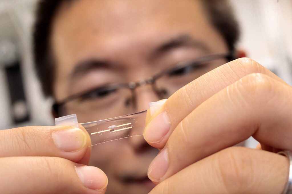
It’s a brainy Band-Aid, a smart watch without the watch, and a leap forward for wearable health technologies. Researchers at the University of Chicago’s Pritzker School of Molecular Engineering (PME) have developed a flexible, stretchable computing chip that processes information by mimicking the human brain. The device, described in the journal Matter, aims to change the way health data is processed.

“With this work we’ve bridged wearable technology with artificial intelligence and machine learning to create a powerful device which can analyze health data right on our own bodies,” said Sihong Wang, a materials scientist and Assistant Professor of Molecular Engineering.

Today, getting an in-depth profile about your health requires a visit to a hospital or clinic. In the future, Wang said, people’s health could be tracked continuously by wearable electronics that can detect disease even before symptoms appear. Unobtrusive, wearable computing devices are one step toward making this vision a reality. 

A Data Deluge
The future of healthcare that Wang—and many others—envision includes wearable biosensors to track complex indicators of health including levels of oxygen, sugar, metabolites and immune molecules in people’s blood. One of the keys to making these sensors feasible is their ability to conform to the skin. As such skin-like wearable biosensors emerge and begin collecting more and more information in real-time, the analysis becomes exponentially more complex. A single piece of data must be put into the broader perspective of a patient’s history and other health parameters.

Today’s smart phones are not capable of the kind of complex analysis required to learn a patient’s baseline health measurements and pick out important signals of disease. However, cutting-edge artificial intelligence platforms that integrate machine learning to identify patterns in extremely complex datasets can do a better job. But sending information from a device to a centralized AI location is not ideal.

“Sending health data wirelessly is slow and presents a number of privacy concerns,” he said. “It is also incredibly energy inefficient; the more data we start collecting, the more energy these transmissions will start using.”

Skin and Brains
Wang’s team set out to design a chip that could collect data from multiple biosensors and draw conclusions about a person’s health using cutting-edge machine learning approaches. Importantly, they wanted it to be wearable on the body and integrate seamlessly with skin.

“With a smart watch, there’s always a gap,” said Wang. “We wanted something that can achieve very intimate contact and accommodate the movement of skin.”

Wang and his colleagues turned to polymers, which can be used to build semiconductors and electrochemical transistors but also have the ability to stretch and bend. They assembled polymers into a device that allowed the artificial-intelligence-based analysis of health data. Rather than work like a typical computer, the chip— called a neuromorphic computing chip—functions more like a human brain, able to both store and analyze data in an integrated way.

Testing the Technology
To test the utility of their new device, Wang’s group used it to analyze electrocardiogram (ECG) data representing the electrical activity of the human heart. They trained the device to classify ECGs into five categories—healthy or four types of abnormal signals. Then, they tested it on new ECGs. Whether or not the chip was stretched or bent, they showed, it could accurately classify the heartbeats.

More work is needed to test the power of the device in deducing patterns of health and disease. But eventually, it could be used either to send patients or clinicians alerts, or to automatically tweak medications.

“If you can get real-time information on blood pressure, for instance, this device could very intelligently make decisions about when to adjust the patient’s blood pressure medication levels,” said Wang. That kind of automatic feedback loop is already used by some implantable insulin pumps, he added.

He already is planning new iterations of the device to both expand the type of devices with which it can integrate and the types of machine learning algorithms it uses.

“Integration of artificial intelligence with wearable electronics is becoming a very active landscape,” said Wang. “This is not finished research, it’s just a starting point.”

Here’s a link to and a citation for the paper,

Intrinsically stretchable neuromorphic devices for on-body processing of health data with artificial intelligence by Shilei Dai, Yahao Dai, Zixuan Zhao, Jie Xu, Jia Huang, Sihong Wang. Matter DOI:https://doi.org/10.1016/j.matt.2022.07.016 Published: August 04, 2022

This paper is behind a paywall.

New chip for neuromorphic computing runs at a fraction of the energy of today’s systems

An August 17, 2022 news item on Nanowerk announces big (so to speak) claims from a team researching neuromorphic (brainlike) computer chips,

An international team of researchers has designed and built a chip that runs computations directly in memory and can run a wide variety of artificial intelligence (AI) applications–all at a fraction of the energy consumed by computing platforms for general-purpose AI computing.

The NeuRRAM neuromorphic chip brings AI a step closer to running on a broad range of edge devices, disconnected from the cloud, where they can perform sophisticated cognitive tasks anywhere and anytime without relying on a network connection to a centralized server. Applications abound in every corner of the world and every facet of our lives, and range from smart watches, to VR headsets, smart earbuds, smart sensors in factories and rovers for space exploration.

The NeuRRAM chip is not only twice as energy efficient as the state-of-the-art “compute-in-memory” chips, an innovative class of hybrid chips that runs computations in memory, it also delivers results that are just as accurate as conventional digital chips. Conventional AI platforms are a lot bulkier and typically are constrained to using large data servers operating in the cloud.

In addition, the NeuRRAM chip is highly versatile and supports many different neural network models and architectures. As a result, the chip can be used for many different applications, including image recognition and reconstruction as well as voice recognition.

..

An August 17, 2022 University of California at San Diego (UCSD) news release (also on EurekAlert), which originated the news item, provides more detail than usually found in a news release,

“The conventional wisdom is that the higher efficiency of compute-in-memory is at the cost of versatility, but our NeuRRAM chip obtains efficiency while not sacrificing versatility,” said Weier Wan, the paper’s first corresponding author and a recent Ph.D. graduate of Stanford University who worked on the chip while at UC San Diego, where he was co-advised by Gert Cauwenberghs in the Department of Bioengineering. 

The research team, co-led by bioengineers at the University of California San Diego, presents their results in the Aug. 17 [2022] issue of Nature.

Currently, AI computing is both power hungry and computationally expensive. Most AI applications on edge devices involve moving data from the devices to the cloud, where the AI processes and analyzes it. Then the results are moved back to the device. That’s because most edge devices are battery-powered and as a result only have a limited amount of power that can be dedicated to computing. 

By reducing power consumption needed for AI inference at the edge, this NeuRRAM chip could lead to more robust, smarter and accessible edge devices and smarter manufacturing. It could also lead to better data privacy as the transfer of data from devices to the cloud comes with increased security risks. 

On AI chips, moving data from memory to computing units is one major bottleneck. 

“It’s the equivalent of doing an eight-hour commute for a two-hour work day,” Wan said. 

To solve this data transfer issue, researchers used what is known as resistive random-access memory, a type of non-volatile memory that allows for computation directly within memory rather than in separate computing units. RRAM and other emerging memory technologies used as synapse arrays for neuromorphic computing were pioneered in the lab of Philip Wong, Wan’s advisor at Stanford and a main contributor to this work. Computation with RRAM chips is not necessarily new, but generally it leads to a decrease in the accuracy of the computations performed on the chip and a lack of flexibility in the chip’s architecture. 

“Compute-in-memory has been common practice in neuromorphic engineering since it was introduced more than 30 years ago,” Cauwenberghs said.  “What is new with NeuRRAM is that the extreme efficiency now goes together with great flexibility for diverse AI applications with almost no loss in accuracy over standard digital general-purpose compute platforms.”

A carefully crafted methodology was key to the work with multiple levels of “co-optimization” across the abstraction layers of hardware and software, from the design of the chip to its configuration to run various AI tasks. In addition, the team made sure to account for various constraints that span from memory device physics to circuits and network architecture. 

“This chip now provides us with a platform to address these problems across the stack from devices and circuits to algorithms,” said Siddharth Joshi, an assistant professor of computer science and engineering at the University of Notre Dame , who started working on the project as a Ph.D. student and postdoctoral researcher in Cauwenberghs lab at UC San Diego. 

Chip performance

Researchers measured the chip’s energy efficiency by a measure known as energy-delay product, or EDP. EDP combines both the amount of energy consumed for every operation and the amount of times it takes to complete the operation. By this measure, the NeuRRAM chip achieves 1.6 to 2.3 times lower EDP (lower is better) and 7 to 13 times higher computational density than state-of-the-art chips. 

Researchers ran various AI tasks on the chip. It achieved 99% accuracy on a handwritten digit recognition task; 85.7% on an image classification task; and 84.7% on a Google speech command recognition task. In addition, the chip also achieved a 70% reduction in image-reconstruction error on an image-recovery task. These results are comparable to existing digital chips that perform computation under the same bit-precision, but with drastic savings in energy. 

Researchers point out that one key contribution of the paper is that all the results featured are obtained directly on the hardware. In many previous works of compute-in-memory chips, AI benchmark results were often obtained partially by software simulation. 

Next steps include improving architectures and circuits and scaling the design to more advanced technology nodes. Researchers also plan to tackle other applications, such as spiking neural networks.

“We can do better at the device level, improve circuit design to implement additional features and address diverse applications with our dynamic NeuRRAM platform,” said Rajkumar Kubendran, an assistant professor for the University of Pittsburgh, who started work on the project while a Ph.D. student in Cauwenberghs’ research group at UC San Diego.

In addition, Wan is a founding member of a startup that works on productizing the compute-in-memory technology. “As a researcher and  an engineer, my ambition is to bring research innovations from labs into practical use,” Wan said. 

New architecture 

The key to NeuRRAM’s energy efficiency is an innovative method to sense output in memory. Conventional approaches use voltage as input and measure current as the result. But this leads to the need for more complex and more power hungry circuits. In NeuRRAM, the team engineered a neuron circuit that senses voltage and performs analog-to-digital conversion in an energy efficient manner. This voltage-mode sensing can activate all the rows and all the columns of an RRAM array in a single computing cycle, allowing higher parallelism. 

In the NeuRRAM architecture, CMOS neuron circuits are physically interleaved with RRAM weights. It differs from conventional designs where CMOS circuits are typically on the peripheral of RRAM weights.The neuron’s connections with the RRAM array can be configured to serve as either input or output of the neuron. This allows neural network inference in various data flow directions without incurring overheads in area or power consumption. This in turn makes the architecture easier to reconfigure. 

To make sure that accuracy of the AI computations can be preserved across various neural network architectures, researchers developed a set of hardware algorithm co-optimization techniques. The techniques were verified on various neural networks including convolutional neural networks, long short-term memory, and restricted Boltzmann machines. 

As a neuromorphic AI chip, NeuroRRAM performs parallel distributed processing across 48 neurosynaptic cores. To simultaneously achieve high versatility and high efficiency, NeuRRAM supports data-parallelism by mapping a layer in the neural network model onto multiple cores for parallel inference on multiple data. Also, NeuRRAM offers model-parallelism by mapping different layers of a model onto different cores and performing inference in a pipelined fashion.

An international research team

The work is the result of an international team of researchers. 

The UC San Diego team designed the CMOS circuits that implement the neural functions interfacing with the RRAM arrays to support the synaptic functions in the chip’s architecture, for high efficiency and versatility. Wan, working closely with the entire team, implemented the design; characterized the chip; trained the AI models; and executed the experiments. Wan also developed a software toolchain that maps AI applications onto the chip. 

The RRAM synapse array and its operating conditions were extensively characterized and optimized at Stanford University. 

The RRAM array was fabricated and integrated onto CMOS at Tsinghua University. 

The Team at Notre Dame contributed to both the design and architecture of the chip and the subsequent machine learning model design and training.

The research started as part of the National Science Foundation funded Expeditions in Computing project on Visual Cortex on Silicon at Penn State University, with continued funding support from the Office of Naval Research Science of AI program, the Semiconductor Research Corporation and DARPA [{US} Defense Advanced Research Projects Agency] JUMP program, and Western Digital Corporation. 

Here’s a link to and a citation for the paper,

A compute-in-memory chip based on resistive random-access memory by Weier Wan, Rajkumar Kubendran, Clemens Schaefer, Sukru Burc Eryilmaz, Wenqiang Zhang, Dabin Wu, Stephen Deiss, Priyanka Raina, He Qian, Bin Gao, Siddharth Joshi, Huaqiang Wu, H.-S. Philip Wong & Gert Cauwenberghs. Nature volume 608, pages 504–512 (2022) DOI: https://doi.org/10.1038/s41586-022-04992-8 Published: 17 August 2022 Issue Date: 18 August 2022

This paper is open access.

Reconfiguring a LEGO-like AI chip with light

MIT engineers have created a reconfigurable AI chip that comprises alternating layers of sensing and processing elements that can communicate with each other. Credit: Figure courtesy of the researchers and edited by MIT News

This image certainly challenges any ideas I have about what Lego looks like. It seems they see things differently at the Massachusetts Institute of Technology (MIT). From a June 13, 2022 MIT news release (also on EurekAlert),

Imagine a more sustainable future, where cellphones, smartwatches, and other wearable devices don’t have to be shelved or discarded for a newer model. Instead, they could be upgraded with the latest sensors and processors that would snap onto a device’s internal chip — like LEGO bricks incorporated into an existing build. Such reconfigurable chipware could keep devices up to date while reducing our electronic waste. 

Now MIT engineers have taken a step toward that modular vision with a LEGO-like design for a stackable, reconfigurable artificial intelligence chip.

The design comprises alternating layers of sensing and processing elements, along with light-emitting diodes (LED) that allow for the chip’s layers to communicate optically. Other modular chip designs employ conventional wiring to relay signals between layers. Such intricate connections are difficult if not impossible to sever and rewire, making such stackable designs not reconfigurable.

The MIT design uses light, rather than physical wires, to transmit information through the chip. The chip can therefore be reconfigured, with layers that can be swapped out or stacked on, for instance to add new sensors or updated processors.

“You can add as many computing layers and sensors as you want, such as for light, pressure, and even smell,” says MIT postdoc Jihoon Kang. “We call this a LEGO-like reconfigurable AI chip because it has unlimited expandability depending on the combination of layers.”

The researchers are eager to apply the design to edge computing devices — self-sufficient sensors and other electronics that work independently from any central or distributed resources such as supercomputers or cloud-based computing.

“As we enter the era of the internet of things based on sensor networks, demand for multifunctioning edge-computing devices will expand dramatically,” says Jeehwan Kim, associate professor of mechanical engineering at MIT. “Our proposed hardware architecture will provide high versatility of edge computing in the future.”

The team’s results are published today in Nature Electronics. In addition to Kim and Kang, MIT authors include co-first authors Chanyeol Choi, Hyunseok Kim, and Min-Kyu Song, and contributing authors Hanwool Yeon, Celesta Chang, Jun Min Suh, Jiho Shin, Kuangye Lu, Bo-In Park, Yeongin Kim, Han Eol Lee, Doyoon Lee, Subeen Pang, Sang-Hoon Bae, Hun S. Kum, and Peng Lin, along with collaborators from Harvard University, Tsinghua University, Zhejiang University, and elsewhere.

Lighting the way

The team’s design is currently configured to carry out basic image-recognition tasks. It does so via a layering of image sensors, LEDs, and processors made from artificial synapses — arrays of memory resistors, or “memristors,” that the team previously developed, which together function as a physical neural network, or “brain-on-a-chip.” Each array can be trained to process and classify signals directly on a chip, without the need for external software or an Internet connection.

In their new chip design, the researchers paired image sensors with artificial synapse arrays, each of which they trained to recognize certain letters — in this case, M, I, and T. While a conventional approach would be to relay a sensor’s signals to a processor via physical wires, the team instead fabricated an optical system between each sensor and artificial synapse array to enable communication between the layers, without requiring a physical connection. 

“Other chips are physically wired through metal, which makes them hard to rewire and redesign, so you’d need to make a new chip if you wanted to add any new function,” says MIT postdoc Hyunseok Kim. “We replaced that physical wire connection with an optical communication system, which gives us the freedom to stack and add chips the way we want.”

The team’s optical communication system consists of paired photodetectors and LEDs, each patterned with tiny pixels. Photodetectors constitute an image sensor for receiving data, and LEDs to transmit data to the next layer. As a signal (for instance an image of a letter) reaches the image sensor, the image’s light pattern encodes a certain configuration of LED pixels, which in turn stimulates another layer of photodetectors, along with an artificial synapse array, which classifies the signal based on the pattern and strength of the incoming LED light.

Stacking up

The team fabricated a single chip, with a computing core measuring about 4 square millimeters, or about the size of a piece of confetti. The chip is stacked with three image recognition “blocks,” each comprising an image sensor, optical communication layer, and artificial synapse array for classifying one of three letters, M, I, or T. They then shone a pixellated image of random letters onto the chip and measured the electrical current that each neural network array produced in response. (The larger the current, the larger the chance that the image is indeed the letter that the particular array is trained to recognize.)

The team found that the chip correctly classified clear images of each letter, but it was less able to distinguish between blurry images, for instance between I and T. However, the researchers were able to quickly swap out the chip’s processing layer for a better “denoising” processor, and found the chip then accurately identified the images.

“We showed stackability, replaceability, and the ability to insert a new function into the chip,” notes MIT postdoc Min-Kyu Song.

The researchers plan to add more sensing and processing capabilities to the chip, and they envision the applications to be boundless.

“We can add layers to a cellphone’s camera so it could recognize more complex images, or makes these into healthcare monitors that can be embedded in wearable electronic skin,” offers Choi, who along with Kim previously developed a “smart” skin for monitoring vital signs.

Another idea, he adds, is for modular chips, built into electronics, that consumers can choose to build up with the latest sensor and processor “bricks.”

“We can make a general chip platform, and each layer could be sold separately like a video game,” Jeehwan Kim says. “We could make different types of neural networks, like for image or voice recognition, and let the customer choose what they want, and add to an existing chip like a LEGO.”

This research was supported, in part, by the Ministry of Trade, Industry, and Energy (MOTIE) from South Korea; the Korea Institute of Science and Technology (KIST); and the Samsung Global Research Outreach Program.

Here’s a link to and a citation for the paper,

Reconfigurable heterogeneous integration using stackable chips with embedded artificial intelligence by Chanyeol Choi, Hyunseok Kim, Ji-Hoon Kang, Min-Kyu Song, Hanwool Yeon, Celesta S. Chang, Jun Min Suh, Jiho Shin, Kuangye Lu, Bo-In Park, Yeongin Kim, Han Eol Lee, Doyoon Lee, Jaeyong Lee, Ikbeom Jang, Subeen Pang, Kanghyun Ryu, Sang-Hoon Bae, Yifan Nie, Hyun S. Kum, Min-Chul Park, Suyoun Lee, Hyung-Jun Kim, Huaqiang Wu, Peng Lin & Jeehwan Kim. Nature Electronics volume 5, pages 386–393 (2022) 05 May 2022 Issue Date: June 2022 Published: 13 June 2022 DOI: https://doi.org/10.1038/s41928-022-00778-y

This paper is behind a paywall.

Speaking in Color, an AI-powered paint tool

This June 16, 2022 article by Jeff Beer for Fast Company took me in an unexpected direction but first, there’s this from Beer’s story,

If an architect wanted to create a building that matched the color of a New York City summer sunset, they’d have to pore over potentially hundreds of color cards designed for industry to get anything close, and still it’d be a tall order to find that exact match. But a new AI-powered, voice-controlled tool from Sherwin-Williams aims to change that.

The paint brand recently launched Speaking in Color, a tool that allows users to tell it about certain places, objects, or shades in order to arrive at that perfect color. You start with a broad description like, say, “New York City summer sunset,” and then fine tune from there once it responds with photos and other options with more in-depth preferences like “darker red,” “make it moodier,” or “add a sliver of sun,” until it’s done.

Developed with agency Wunderman Thompson, it’s a React web app that uses natural language to find your preferred color using both third-party and proprietary code. The tool’s custom algorithm allows you to tweak colors in a way that translates statements like “make it dimmer,” “add warmth,” or “more like the 1980s” into mathematical adjustments.

It seems to me Wunderman Thompson needs to rethink its Sherwin Williams Speaking in Color promotional video (it’s embedded with Beer’s June 16, 2022 article or you can find it here; scroll down about 50% of the way). You’ll note, the color prompts are not spoken; they’re in text, e.g., ‘crystal-clear Caribbean ocean’. So much for ‘speaking in color’ but the article aroused my curiosity which is how I found this May 19, 2017 article by Annalee Newitz for Ars Technica highlighting another color/AI project (Note: A link has been removed),

At some point, we’ve all wondered about the incredibly strange names for paint colors. Research scientist and neural network goofball Janelle Shane took the wondering a step further. Shane decided to train a neural network to generate new paint colors, complete with appropriate names. The results are possibly the greatest work of artificial intelligence I’ve seen to date.

Writes Shane on her Tumblr, “For this experiment, I gave the neural network a list of about 7,700 Sherwin-Williams paint colors along with their RGB values. (RGB = red, green, and blue color values.) Could the neural network learn to invent new paint colors and give them attractive names?”

Shane told Ars that she chose a neural network algorithm called char-rnn, which predicts the next character in a sequence. So basically the algorithm was working on two tasks: coming up with sequences of letters to form color names, and coming up with sequences of numbers that map to an RGB value. As she checked in on the algorithm’s progress, she found that it was able to create colors long before it could actually name them reliably.

The longer it processed the dataset, the closer the algorithm got to making legit color names, though they were still mostly surreal: “Soreer Gray” is a kind of greenish color, and “Sane Green” is a purplish blue. When Shane cranked up “creativity” on the algorithm’s output, it gave her a violet color called “Dondarf” and a Kelly green called “Bylfgoam Glosd.” After churning through several more iterations of this process, Shane was able to get the algorithm to recognize some basic colors like red and gray, “though not reliably,” because she also gets a sky blue called “Gray Pubic” and a dark green called “Stoomy Brown.”

Brown has since written a book about artificial intelligence (You Look Like a Thing and I Love You; How Artificial Intelligence Works and Why It’s Making the World a Weirder Place [2019]) and continues her investigations of AI. You can find her website and blog here and her Wikipedia entry here.

Cambodian sci-fi movie exploring Buddhism and nanotechnology

The movie is ‘Karmalink’. From its Internet Movie Datavase (IMDb) entry,

In this Buddhist sci-fi mystery set in near-future Phnom Penh, a young Cambodian detective untangles a link between her friend’s past-life dreams of a lost gold artifact and a neuroscientist’s determination to attain digital enlightenment.

Craig C Lewis’ June 10, 2022 article on buddhistdoor.net offers both illumination and puzzlement,

Cambodian Sci-Fi Movie Karmalink Explores Enlightenment, Reincarnation, and Nanotechnology

The Cambodian science fiction move Karmalink, which won awards on its film festival debut last year for its intriguing mix of high-tech mystery and Buddhist philosophy, has released a new trailer ahead of its North American release next month.

“In near-future Phnom Penh, a teenage boy teams up with a street-smart girl from his neighborhood to untangle the mystery of his past-life dreams,” a synopsis on the website of executive producer Valerie Steinberg explains. “What begins as a hunt for a Buddhist treasure soon leads to greater discoveries that will either end in digital enlightenment or a total loss of identity.” (Valerie Steinberg)

Directed and co-written by Jake Wachtel, Karmalink’s story is set in the Cambodian capital Phnom Penh, and sets out to explore the intersection of the Buddhist themes of karma, reincarnation, and enlightenment with the consciousness-altering implications of augmented reality and artificial intelligence, as well as the growing disparity between rich and poor.

The main plot follows a 13-year-old boy, Leng Heng (Leng Heng Prak), and his friend, Srey Leak (Srey Leak Chhith), who live in a crowded, dilapidated community on the outskirts of Phnom Penh of the near future.

Heng has been having a recurring dream about a golden Buddha statue owned by various people who he believes to be his past incarnations. Heng enlists the help of Leak to untangle the links between his dreams and the aspirations of a prominent neuroscientist to attain digital enlightenment via nanotechnology [emphasis mine] in order to find the truth and discover their own destiny.

Unfortunately, there are no more details as to how nanotechnology helps with attaining ‘digital enlightenment’. As to what digital enlightenment might be, that too is a mystery.

Matt Villei’s June 9 (?), 2022 article for collider.com provides more details about the movie and its trailer/preview,

The trailer is made up of the many rewards and snippets that the film received during its film festival run, which started in September 2021 at that year’s Venice’s International Film Critic’s Week. It was also announced a few days ago that it will be released theatrically in major US cities as well as Video On Demand in both the US and Canada on July 15, 2022. The film is spoken in Khmer with English subtitles and is a total of 102 minutes long. The film was created as a way to “interrogate processes of neo-colonialism, and highlighting the alienating effects of technological progress, Jake Wachtel’s Karmalink is a mind-bending tale of reincarnation, artificial consciousness, and the search for enlightenment.”

Sadly, the lead actor, Leng Heng Prak, has died since production of the film.

You may want to keep an eye out for Karmalink.

Art and 5G at museums in Turin (Italy)

Caption: In the framework of EU-funded project 5GTours, R1 humanoid robot tested at GAM (Turin) its ability to navigate and interact with visitors at the 20th-century collections, accompanying them to explore a selection of the museum’s most representative works, such as Andy Warhol’s “Orange car crash”. The robot has been designed and developed by IIT, while the 5G connection was set up by TIM using Ericsson technology.. Credit: IIT-Istituto Italiano di Tecnologia/GAM

This May 27, 2022 Istituto Italiano di Tecnologia (IIT) press release on EurekAlert offers an intriguing view into the potential for robots in art galleries,

Robotics, 5G and art: during the month of May visitors to the Turin’s art museums, Turin Civic Gallery of Modern and Contemporary Art (GAM) and Turin City Museum of Ancient Art (Palazzo Madama), had the opportunity to be part of various experiments based on 5G-network technology. Interactive technologies and robots were the focus of an innovative enjoyment of the art collections, with a great appreciation from the public.

Visitors to the GAM and to Palazzo Madama were provided with a number of engaging interactive experiences made possible through a significant collaboration between public and private organisations, which have been working together for more than three years to experiment the potential of new 5G technology in the framework of the EU-funded project 5GTours (https://5gtours.eu/).

The demonstrations set up in Turin led to the creation of innovative applications in the tourism and culture sectors that can easily be replicated in any artistic or museum context.

In both venues, visitors had the opportunity to meet R1, the humanoid robot designed by the IIT-Istituto Italiano di Tecnologia (Italian Institute of Technology) in Genova and created to operate in domestic and professional environments, whose autonomous and remote navigation system is well integrated with the bandwidth and latency offered by a 5G connection. R1, the robot – 1 metre 25 cm in height, weighing 50 kg, made 50% from plastic and 50% from carbon fibre and metal – is able to describe the works and answer questions regarding the artist or the period in history to which the work belongs. 5G connectivity is required in order to transmit the considerable quantity of data generated by the robot’s sensors and the algorithms that handle environmental perception, autonomous navigation and dialogue to external processing systems with extremely rapid response times.

At Palazzo Madama R1 humanoid robot led a guided tour of the Ceramics Room, while at GAM it was available to visitors of the twentieth-century collections, accompanying them to explore a selection of the museum’s most representative works. R1 robot explained and responded to questions about six relevant paintings: Felice Casorati’s “Daphne a Pavarolo”, Osvaldo Lucini’s “Uccello 2”, Marc Chagall’s “Dans mon pays”, Alberto Burri’s “Sacco”, Andy Warhol’s “Orange car crash” and Mario Merz’s “Che Fare?”.

Moreover, visitors – with the use of Meta Quest visors also connected to the 5G network – were required to solve a puzzle, putting the paintings in the Guards’ Room back into their frames. With these devices, the works in the hall, which in reality cannot be touched, can be handled and moved virtually. Lastly, the visitors involved had the opportunity to visit the underground spaces of Palazzo Madama with the mini-robot Double 3, which uses the 5G network to move reactively and precisely within the narrow spaces.

At GAM a class of students from a local school were able to remotely connect and manoeuvre the mini-robot Double 3 located in the rooms of the twentieth-century collections at the GAM directly from their classroom. A treasure hunt held in the museum with the participants never leaving the school.

In the Educational Area, a group of youngsters had the opportunity of collaborating in the painting of a virtual work of art on a large technological wall, drawing inspiration from works by Nicola De Maria.

The 5G network solutions created at the GAM and at Palazzo Madama by TIM [Telecom Italia] with Ericsson technology in collaboration with the City of Turin and the Turin Museum Foundation, guarantee constant high-speed transmission and extremely low latency. These solutions, which comply with 3GPP standard, are extremely flexible in terms of setting up and use. In the case of Palazzo Madama, a UNESCO World Heritage Site, tailor-made installations were designed, using apparatus and solutions that perfectly integrate with the museum spaces, while at the same time guaranteeing extremely high performance. At the GAM, the Radio Dot System has been implemented, a new 5G solution from Ericsson that is small enough to be held in the palm of a hand, and that provides network coverage and performance required for busy indoor areas. Thanks to these activities, Turin is ever increasingly playing a role as an open-air laboratory for urban innovation; since 2021 it has been the location of the “House of Emerging Technology – CTE NEXT”, a veritable centre for technology transfer via 5G and for emerging technologies coordinated by the Municipality of Turin and financed by the Ministry for Economic Development.

Through these solutions, Palazzo Madama and the GAM are now unique examples of technology in Italy and a rare example on a European level of museum buildings with full 5G coverage.

The experience was the result of the project financed by the European Union, 5G-TOURS 5G smarT mObility, media and e-health for toURists and citizenS”, the city of Turin – Department and Directorate of Innovation, in collaboration with the Department of Culture – Ericsson, TIM [Telecom Italia], the Turin Museum Foundation and the IIT-Istituto Italiano di Tecnologia (Italian Institute of Technology) of Genova, with the contribution of the international partners Atos and Samsung. The 5G coverage within the two museums was set up by TIM using Ericsson technology, solutions that perfectly integrated with the areas within the two museums structures.

Just in case you missed the link in the press release, you can find more information about this European Union Horizon 2020-funded 5G project, here at 5G TOURS (SmarT mObility, media and e-health for toURists and citizenS). You can find out more about the grant, e.g., this project sunset in July 2022, here.

How AI-designed fiction reading lists and self-publishing help nurture far-right and neo-Nazi novelists

Literary theorists Helen Young and Geoff M Boucher, both at Deakin University (Australia), have co-written a fascinating May 29, 2022 essay on The Conversation (and republished on phys.org) analyzing some of the reasons (e.g., novels) for the resurgence in neo-Nazi activity and far-right extremism, Note: Links have been removed,

Far-right extremists pose an increasing risk in Australia and around the world. In 2020, ASIO [Australian Security Intelligence Organisation] revealed that about 40% of its counter-terrorism work involved the far right.

The recent mass murder in Buffalo, U.S., and the attack in Christchurch, New Zealand, in 2019 are just two examples of many far-right extremist acts of terror.

Far-right extremists have complex and diverse methods for spreading their messages of hate. These can include through social media, video games, wellness culture, interest in medieval European history, and fiction [emphasis mine]. Novels by both extremist and non-extremist authors feature on far-right “reading lists” designed to draw people into their beliefs and normalize hate.

Here’s more about how the books get published and distributed, from the May 29, 2022 essay, Note: Links have been removed,

Publishing houses once refused to print such books, but changes in technology have made traditional publishers less important. With self-publishing and e-books, it is easy for extremists to produce and distribute their fiction.

In this article, we have only given the titles and authors of those books that are already notorious, to avoid publicizing other dangerous hate-filled fictions.

Why would far-right extremists write novels?

Reading fiction is different to reading non-fiction. Fiction offers readers imaginative scenarios that can seem to be truthful, even though they are not fact-based. It can encourage readers to empathize with the emotions, thoughts and ethics of characters, particularly when they recognize those characters as being “like” them.

A novel featuring characters who become radicalized to far-right extremism, or who undertake violent terrorist acts, can help make those things seem justified and normal.

Novels that promote political violence, such as The Turner Diaries, are also ways for extremists to share plans and give readers who hold extreme views ideas about how to commit terrorist acts. …

In the late 20th century, far-right extremists without Pierce’s notoriety [American neo-Nazi William L. Pierce published The Turner Diaries (1978)] found it impossible to get their books published. One complained about this on his blog in 1999, blaming feminists and Jewish people. Just a few years later, print-on-demand and digital self-publishing made it possible to circumvent this difficulty.

The same neo-Nazi self-published what he termed “a lifetime of writing” in the space of a few years in the early 2000s. The company he paid to produce his books—iUniverse.com—helped get them onto the sales lists of major booksellers Barnes and Noble and Amazon in the early 2000s, making a huge difference to how easily they circulated outside extremist circles.

It still produces print-on-demand hard copies, even though the author has died. The same author’s books also circulate in digital versions, including on Google Play and Kindle, making them easily accessible.

Distributing extremist novels digitally

Far-right extremists use social media to spread their beliefs, but other digital platforms are also useful for them.

Seemingly innocent sites that host a wide range of mainstream material, such as Google Books, Project Gutenberg, and the Internet Archive, are open to exploitation. Extremists use them to share, for example, material denying the Holocaust alongside historical Nazi newspapers.

Amazon’s Kindle self-publishing service has been called “a haven for white supremacists” because of how easy it is for them to circulate political tracts there. The far-right extremist who committed the Oslo terrorist attacks in 2011 recommended in his manifesto that his followers use Kindle to to spread his message.

Our research has shown that novels by known far-right extremists have been published and circulated through Kindle as well as other digital self-publishing services.

Ai and its algorithms also play a role, from the May 29, 2022 essay,

Radicalising recommendations

As we researched how novels by known violent extremists circulate, we noticed that the sales algorithms of mainstream platforms were suggesting others that we might also be interested in. Sales algorithms work by recommending items that customers who purchased one book have also viewed or bought.

Those recommendations directed us to an array of novels that, when we investigated them, proved to resonate with far-right ideologies.

A significant number of them were by authors with far-right political views. Some had ties to US militia movements and the gun-obsessed “prepper” subculture. Almost all of the books were self-published as e-books and print-on-demand editions.

Without the marketing and distribution channels of established publishing houses, these books rely on digital circulation for sales, including sale recommendation algorithms.

The trail of sales recommendations led us, with just two clicks, to the novels of mainstream authors. They also led us back again, from mainstream authors’ books to extremist novels. This is deeply troubling. It risks unsuspecting readers being introduced to the ideologies, world-views and sometimes powerful emotional narratives of far-right extremist novels designed to radicalise.

It’s not always easy to tell right away if you’re reading fiction promoting far-right ideologies, from the May 29, 2022 essay,

Recognising far-right messages

Some extremist novels follow the lead of The Turner Diaries and represent the start of a racist, openly genocidal war alongside a call to bring one about. Others are less obvious about their violent messages.

Some are not easily distinguished from mainstream novels – for example, from political thrillers and dystopian adventure stories like those of Tom Clancy or Matthew Reilly – so what is different about them? Openly neo-Nazi authors, like Pierce, often use racist, homophobic and misogynist slurs, but many do not. This may be to help make their books more palatable to general readers, or to avoid digital moderation based on specific words.

Knowing more about far-right extremism can help. Researchers generally say that there are three main things that connect the spectrum of far-right extremist politics: acceptance of social inequality, authoritarianism, and embracing violence as a tool for political change. Willingness to commit or endorse violence is a key factor separating extremism from other radical politics.

It is very unlikely that anyone would become radicalised to violent extremism just by reading novels. Novels can, however, reinforce political messages heard elsewhere (such as on social media) and help make those messages and acts of hate feel justified.

With the growing threat of far-right extremism and deliberate recruitment strategies of extremists targeting unexpected places, it is well worth being informed enough to recognise the hate-filled stories they tell.

I recommend reading the essay as my excerpts don’t do justice to the ideas being presented. As Young and Boucher note, it’s “… unlikely that anyone would become radicalised to violent extremism …” by reading novels but far-right extremists and neo-Nazis write fiction because the tactic works at some level.

Smart City tech brief: facial recognition, cybersecurity; privacy protection; and transparency

This May 10, 2022 Association for Computing Machinery (ACM) announcement (received via email) has an eye-catching head,

Should Smart Cities Adopt Facial Recognition, Remote Monitoring Software+Social Media to Police [verb] Info?

The Association for Computing Machinery, the largest and most prestigious computer science society worldwide (100,000 members) has released a report, ACM TechBrief: Smart Cities, for smart city planners to address 1) cybersecurity; 2) privacy protections; 3) fairness and transparency; and 4) sustainability when planning and designing systems, including climate impact. 

There’s a May 3, 2022 ACM news release about the latest technical brief,

The Association for Computing Machinery’s global Technology Policy Council (ACM TPC) just released, “ACM TechBrief: Smart Cities,” which highlights the challenges involved in deploying information and communication technology to create smart cities and calls for policy leaders planning such projects to do so without compromising security, privacy, fairness and sustainability. The TechBrief includes a primer on smart cities, key statistics about the growth and use of these technologies, and a short list of important policy implications.

“Smart cities” are municipalities that use a network of physical devices and computer technologies to make the delivery of public services more efficient and/or more environmentally friendly. Examples of smart city applications include using sensors to turn off streetlights when no one is present, monitoring traffic patterns to reduce roadway congestion and air pollution, or keeping track of home-bound medical patients in order to dispatch emergency responders when needed. Smart cities are an outgrowth of the Internet of Things (IoT), the rapidly growing infrastructure of literally billions of physical devices embedded with sensors that are connected to computers and the Internet.

The deployment of smart city technology is growing across the world, and these technologies offer significant benefits. For example, the TechBrief notes that “investing in smart cities could contribute significantly to achieving greenhouse gas emissions reduction targets,” and that “smart cities use digital innovation to make urban service delivery more efficient.”

Because of the meteoric growth and clear benefits of smart city technologies, the TechBrief notes that now is an urgent time to address some of the important public policy concerns that smart city technologies raise. The TechBrief lists four key policy implications that government officials, as well as the private companies that develop these technologies, should consider.

These include:

Cybersecurity risks must be considered at every stage of every smart city technology’s life cycle.

Effective privacy protection mechanisms must be an essential component of any smart city technology deployed.

Such mechanisms should be transparently fair to all city users, not just residents.

The climate impact of smart city infrastructures must be fully understood as they are being designed and regularly assessed after they are deployed

“Smart cities are fast becoming a reality around the world,”explains Chris Hankin, a Professor at Imperial College London and lead author of the ACM TechBrief on Smart Cities. “By 2025, 26% of all internet-connected devices will be used in a smart city application. As technologists, we feel we have a responsibility to raise important questions to ensure that these technologies best serve the public interest. For example, many people are unaware that some smart city technologies involve the collection of personally identifiable data. We developed this TechBrief to familiarize the public and lawmakers with this topic and present some key issues for consideration. Our overarching goal is to guide enlightened public policy in this area.”

“Our new TechBrief series builds on earlier and ongoing work by ACM’s technology policy committees,” added James Hendler, Professor at Rensselaer Polytechnic Institute and Chair of the ACM Technology Policy Council. “Because many smart city applications involve algorithms making decisions which impact people directly, this TechBrief calls for methods to ensure fairness and transparency in how these systems are developed. This reinforces an earlier statement we issued that outlined seven principles for algorithmic transparency and accountability. We also note that smart city infrastructures are especially vulnerable to malicious attacks.”

This TechBrief is the third in a series of short technical bulletins by ACM TPC that present scientifically grounded perspectives on the impact of specific developments or applications of technology. Designed to complement ACM’s activities in the policy arena, TechBriefs aim to inform policymakers, the public, and others about the nature and implications of information technologies. The first ACM TechBrief focused on climate change, while the second addressed facial recognition. Topics under consideration for future issues include quantum computing, election security, and encryption.

About the ACM Technology Policy Council

ACM’s global Technology Policy Council sets the agenda for ACM’s global policy activities and serves as the central convening point for ACM’s interactions with government organizations, the computing community, and the public in all matters of public policy related to computing and information technology. The Council’s members are drawn from ACM’s global membership. It coordinates the activities of ACM’s regional technology policy groups and sets the agenda for global initiatives to address evolving technology policy issues.

About ACM

ACM, the Association for Computing Machinery, is the world’s largest educational and scientific computing society, uniting educators, researchers and professionals to inspire dialogue, share resources and address the field’s challenges. ACM strengthens the computing profession’s collective voice through strong leadership, promotion of the highest standards, and recognition of technical excellence. ACM supports the professional growth of its members by providing opportunities for life-long learning, career development, and professional networking.

This is indeed a brief. I recommend reading it as it provides a very good overview to the topic of ‘smart cities’ and raises a question or two. For example, there’s this passage from the April 2022 Issue 3 Technical Brief on p. 2,

… policy makers should target broad and fair access and application of AI and, in general, ICT [information and communication technologies]. This can be achieved through transparent planning and decision-making processes for smart city infrastructure and application developments, such as open hearings, focus groups, and advisory panels. The goal must be to minimize potential harm while maximizing the benefits that algorithmic decision-making [emphasis mine] can bring

Is this algorithmic decision-making under human supervision? It doesn’t seem to be specified in the brief itself. It’s possible the answer lies elsewhere. After all, this is the third in the series.

Tiny nanomagnets interact like neurons in the brain for low energy artificial intelligence (brainlike) computing

Saving energy is one of the main drivers for the current race to make neuromorphic (brainlike) computers as this May 5, 2022 news item on Nanowerk comments, Note: Links have been removed,

Researchers have shown it is possible to perform artificial intelligence using tiny nanomagnets that interact like neurons in the brain.

The new method, developed by a team led by Imperial College London researchers, could slash the energy cost of artificial intelligence (AI), which is currently doubling globally every 3.5 months. [emphasis mine]

In a paper published in Nature Nanotechnology (“Reconfigurable training and reservoir computing in an artificial spin-vortex ice via spin-wave fingerprinting”), the international team have produced the first proof that networks of nanomagnets can be used to perform AI-like processing. The researchers showed nanomagnets can be used for ‘time-series prediction’ tasks, such as predicting and regulating insulin levels in diabetic patients.

A May 5, 2022 Imperial College London (ICL) press release (also on EurekAlert) by Hayley Dunning, which originated the news item delves further into the research,

Artificial intelligence that uses ‘neural networks’ aims to replicate the way parts of the brain work, where neurons talk to each other to process and retain information. A lot of the maths used to power neural networks was originally invented by physicists to describe the way magnets interact, but at the time it was too difficult to use magnets directly as researchers didn’t know how to put data in and get information out.

Instead, software run on traditional silicon-based computers was used to simulate the magnet interactions, in turn simulating the brain. Now, the team have been able to use the magnets themselves to process and store data – cutting out the middleman of the software simulation and potentially offering enormous energy savings.

Nanomagnetic states

Nanomagnets can come in various ‘states’, depending on their direction. Applying a magnetic field to a network of nanomagnets changes the state of the magnets based on the properties of the input field, but also on the states of surrounding magnets.

The team, led by Imperial Department of Physics researchers, were then able to design a technique to count the number of magnets in each state once the field has passed through, giving the ‘answer’.

Co-first author of the study Dr Jack Gartside said: “We’ve been trying to crack the problem of how to input data, ask a question, and get an answer out of magnetic computing for a long time. Now we’ve proven it can be done, it paves the way for getting rid of the computer software that does the energy-intensive simulation.”

Co-first author Kilian Stenning added: “How the magnets interact gives us all the information we need; the laws of physics themselves become the computer.”

Team leader Dr Will Branford said: “It has been a long-term goal to realise computer hardware inspired by the software algorithms of Sherrington and Kirkpatrick. It was not possible using the spins on atoms in conventional magnets, but by scaling up the spins into nanopatterned arrays we have been able to achieve the necessary control and readout.”

Slashing energy cost

AI is now used in a range of contexts, from voice recognition to self-driving cars. But training AI to do even relatively simple tasks can take huge amounts of energy. For example, training AI to solve a Rubik’s cube took the energy equivalent of two nuclear power stations running for an hour.

Much of the energy used to achieve this in conventional, silicon-chip computers is wasted in inefficient transport of electrons during processing and memory storage. Nanomagnets however don’t rely on the physical transport of particles like electrons, but instead process and transfer information in the form of a ‘magnon’ wave, where each magnet affects the state of neighbouring magnets.

This means much less energy is lost, and that the processing and storage of information can be done together, rather than being separate processes as in conventional computers. This innovation could make nanomagnetic computing up to 100,000 times more efficient than conventional computing.

AI at the edge

The team will next teach the system using real-world data, such as ECG signals, and hope to make it into a real computing device. Eventually, magnetic systems could be integrated into conventional computers to improve energy efficiency for intense processing tasks.

Their energy efficiency also means they could feasibly be powered by renewable energy, and used to do ‘AI at the edge’ – processing the data where it is being collected, such as weather stations in Antarctica, rather than sending it back to large data centres.

It also means they could be used on wearable devices to process biometric data on the body, such as predicting and regulating insulin levels for diabetic people or detecting abnormal heartbeats.

Here’s a link to and a citation for the paper,

Reconfigurable training and reservoir computing in an artificial spin-vortex ice via spin-wave fingerprinting by Jack C. Gartside, Kilian D. Stenning, Alex Vanstone, Holly H. Holder, Daan M. Arroo, Troy Dion, Francesco Caravelli, Hidekazu Kurebayashi & Will R. Branford. Nature Nanotechnology (2022) DOI: https://doi.org/10.1038/s41565-022-01091-7 Published 05 May 2022

This paper is behind a paywall.

Quantum memristors

This March 24, 2022 news item on Nanowerk announcing work on a quantum memristor seems to have had a rough translation from German to English,

In recent years, artificial intelligence has become ubiquitous, with applications such as speech interpretation, image recognition, medical diagnosis, and many more. At the same time, quantum technology has been proven capable of computational power well beyond the reach of even the world’s largest supercomputer.

Physicists at the University of Vienna have now demonstrated a new device, called quantum memristor, which may allow to combine these two worlds, thus unlocking unprecedented capabilities. The experiment, carried out in collaboration with the National Research Council (CNR) and the Politecnico di Milano in Italy, has been realized on an integrated quantum processor operating on single photons.

Caption: Abstract representation of a neural network which is made of photons and has memory capability potentially related to artificial intelligence. Credit: © Equinox Graphics, University of Vienna

A March 24, 2022 University of Vienna (Universität Wien) press release (also on EurekAlert), which originated the news item, explains why this work has an impact on artificial intelligence,

At the heart of all artificial intelligence applications are mathematical models called neural networks. These models are inspired by the biological structure of the human brain, made of interconnected nodes. Just like our brain learns by constantly rearranging the connections between neurons, neural networks can be mathematically trained by tuning their internal structure until they become capable of human-level tasks: recognizing our face, interpreting medical images for diagnosis, even driving our cars. Having integrated devices capable of performing the computations involved in neural networks quickly and efficiently has thus become a major research focus, both academic and industrial.

One of the major game changers in the field was the discovery of the memristor, made in 2008. This device changes its resistance depending on a memory of the past current, hence the name memory-resistor, or memristor. Immediately after its discovery, scientists realized that (among many other applications) the peculiar behavior of memristors was surprisingly similar to that of neural synapses. The memristor has thus become a fundamental building block of neuromorphic architectures.

A group of experimental physicists from the University of Vienna, the National Research Council (CNR) and the Politecnico di Milano led by Prof. Philip Walther and Dr. Roberto Osellame, have now demonstrated that it is possible to engineer a device that has the same behavior as a memristor, while acting on quantum states and being able to encode and transmit quantum information. In other words, a quantum memristor. Realizing such device is challenging because the dynamics of a memristor tends to contradict the typical quantum behavior. 

By using single photons, i.e. single quantum particles of lights, and exploiting their unique ability to propagate simultaneously in a superposition of two or more paths, the physicists have overcome the challenge. In their experiment, single photons propagate along waveguides laser-written on a glass substrate and are guided on a superposition of several paths. One of these paths is used to measure the flux of photons going through the device and this quantity, through a complex electronic feedback scheme, modulates the transmission on the other output, thus achieving the desired memristive behavior. Besides demonstrating the quantum memristor, the researchers have provided simulations showing that optical networks with quantum memristor can be used to learn on both classical and quantum tasks, hinting at the fact that the quantum memristor may be the missing link between artificial intelligence and quantum computing.

“Unlocking the full potential of quantum resources within artificial intelligence is one of the greatest challenges of the current research in quantum physics and computer science”, says Michele Spagnolo, who is first author of the publication in the journal “Nature Photonics”. The group of Philip Walther of the University of Vienna has also recently demonstrated that robots can learn faster when using quantum resources and borrowing schemes from quantum computation. This new achievement represents one more step towards a future where quantum artificial intelligence become reality.

Here’s a link to and a citation for the paper,

Experimental photonic quantum memristor by Michele Spagnolo, Joshua Morris, Simone Piacentini, Michael Antesberger, Francesco Massa, Andrea Crespi, Francesco Ceccarelli, Roberto Osellame & Philip Walther. Nature Photonics volume 16, pages 318–323 (2022) DOI: https://doi.org/10.1038/s41566-022-00973-5 Published 24 March 2022 Issue Date April 2022

This paper is open access.