Caption: The fuel cell’s 3D printed cap peeks above the ground. The cap keeps debris out of the device while enabling air flow. Credit: Bill Yen/Northwestern University
*New fuel cell harnesses naturally occurring microbes to generate electricity
*Soil-powered sensors to successfully monitor soil moisture and detect touch
*New tech was robust enough to withstand drier soil conditions and flooding
*Fuel cell could replace batteries in sensors used for precision agriculture
EVANSTON, Ill. — A Northwestern University-led team of researchers has developed a new fuel cell that harvests energy from microbes living in dirt.
About the size of a standard paperback book, the completely soil-powered technology could fuel underground sensors used in precision agriculture and green infrastructure. This potentially could offer a sustainable, renewable alternative to batteries, which hold toxic, flammable chemicals that leach into the ground, are fraught with conflict-filled supply chains and contribute to the ever-growing problem of electronic waste.
To test the new fuel cell, the researchers used it to power sensors measuring soil moisture and detecting touch, a capability that could be valuable for tracking passing animals. To enable wireless communications, the researchers also equipped the soil-powered sensor with a tiny antenna to transmit data to a neighboring base station by reflecting existing radio frequency signals.
Not only did the fuel cell work in both wet and dry conditions, but its power also outlasted similar technologies by 120%.
The research will be published today (Jan. 12 [2024]) in the Proceedings of the Association for Computing Machinery on Interactive, Mobile, Wearable and Ubiquitous Technologies. The study authors also are releasing all designs, tutorials and simulation tools to the public, so others may use and build upon the research.
“The number of devices in the Internet of Things (IoT) is constantly growing,” said Northwestern alumnus Bill Yen, who led the work. “If we imagine a future with trillions of these devices, we cannot build every one of them out of lithium, heavy metals and toxins that are dangerous to the environment. We need to find alternatives that can provide low amounts of energy to power a decentralized network of devices. In a search for solutions, we looked to soil microbial fuel cells, which use special microbes to break down soil and use that low amount of energy to power sensors. As long as there is organic carbon in the soil for the microbes to break down, the fuel cell can potentially last forever.”
“These microbes are ubiquitous; they already live in soil everywhere,” said Northwestern’s George Wells, a senior author on the study. “We can use very simple engineered systems to capture their electricity. We’re not going to power entire cities with this energy. But we can capture minute amounts of energy to fuel practical, low-power applications.”
Wells is an associate professor of civil and environmental engineering at Northwestern’s McCormick School of Engineering. Now a Ph.D. student at Stanford University, Yen started this project when he was an undergraduate researcher in Wells’ laboratory.
Solutions for a dirty job
In recent years, farmers worldwide increasingly have adopted precision agriculture as a strategy to improve crop yields. The tech-driven approach relies on measuring precise levels of moisture, nutrients and contaminants in soil to make decisions that enhance crop health. This requires a widespread, dispersed network of electronic devices to continuously collect environmental data.
“If you want to put a sensor out in the wild, in a farm or in a wetland, you are constrained to putting a battery in it or harvesting solar energy,” Yen said. “Solar panels don’t work well in dirty environments because they get covered with dirt, do not work when the sun isn’t out and take up a lot of space. Batteries also are challenging because they run out of power. Farmers are not going to go around a 100-acre farm to regularly swap out batteries or dust off solar panels.”
To overcome these challenges, Wells, Yen and their collaborators wondered if they could instead harvest energy from the existing environment. “We could harvest energy from the soil that farmers are monitoring anyway,” Yen said.
‘Stymied efforts’
Making their first appearance in 1911, soil-based microbial fuel cells (MFCs) operate like a battery — with an anode, cathode and electrolyte. But instead of using chemicals to generate electricity, MFCs harvest electricity from bacteria that naturally donate electrons to nearby conductors. When these electrons flow from the anode to the cathode, it creates an electric circuit.
But in order for microbial fuel cells to operate without disruption, they need to stay hydrated and oxygenated — which is tricky when buried underground within dry dirt.
“Although MFCs have existed as a concept for more than a century, their unreliable performance and low output power have stymied efforts to make practical use of them, especially in low-moisture conditions,” Yen said.
Winning geometry
With these challenges in mind, Yen and his team embarked on a two-year journey to develop a practical, reliable soil-based MFC. His expedition included creating — and comparing — four different versions. First, the researchers collected a combined nine months of data on the performance of each design. Then, they tested their final version in an outdoor garden.
The best-performing prototype worked well in dry conditions as well as within a water-logged environment. The secret behind its success: Its geometry. Instead of using a traditional design, in which the anode and cathode are parallel to one another, the winning fuel cell leveraged a perpendicular design.
Made of carbon felt (an inexpensive, abundant conductor to capture the microbes’ electrons), the anode is horizontal to the ground’s surface. Made of an inert, conductive metal, the cathode sits vertically atop the anode.
Although the entire device is buried, the vertical design ensures that the top end is flush with the ground’s surface. A 3D-printed cap rests on top of the device to prevent debris from falling inside. And a hole on top and an empty air chamber running alongside the cathode enable consistent airflow.
The lower end of the cathode remains nestled deep beneath the surface, ensuring that it stays hydrated from the moist, surrounding soil — even when the surface soil dries out in the sunlight. The researchers also coated part of the cathode with waterproofing material to allow it to breathe during a flood. And, after a potential flood, the vertical design enables the cathode to dry out gradually rather than all at once.
On average, the resulting fuel cell generated 68 times more power than needed to operate its sensors. It also was robust enough to withstand large changes in soil moisture — from somewhat dry (41% water by volume) to completely underwater.
Making computing accessible
The researchers say all components for their soil-based MFC can be purchased at a local hardware store. Next, they plan to develop a soil-based MFC made from fully biodegradable materials. Both designs bypass complicated supply chains and avoid using conflict minerals.
“With the COVID-19 pandemic, we all became familiar with how a crisis can disrupt the global supply chain for electronics,” said study co-author Josiah Hester, a former Northwestern faculty member who is now at the Georgia Institute of Technology. “We want to build devices that use local supply chains and low-cost materials so that computing is accessible for all communities.”
The study, “Soil-powered computing: The engineer’s guide to practical soil microbial fuel cell design,” was supported by the National Science Foundation (award number CNS-2038853), the Agricultural and Food Research Initiative (award number 2023-67021-40628) from the USDA National Institute of Food and Agriculture, the Alfred P. Sloan Foundation, VMware Research and 3M.
Here’s a link to and a citation for the paper,
Soil-Powered Computing: The Engineer’s Guide to Practical Soil Microbial Fuel Cell Design by Bill Yen, Laura Jaliff, Louis Gutierrez, Philothei Sahinidis, Sadie Bernstein, John Madden, Stephen Taylor, Colleen Josephson, Pat Pannuto, Weitao Shuai, George Wells, Nivedita Arora, Josiah Hester. Proceedings of the ACM on Interactive, Mobile, Wearable and Ubiquitous Technologies Volume 7 Issue 4 Article No.: 196 pp 1–40 DOI: https://doi.org/10.1145/3631410 Published: 12 January 2024
This May 10, 2022 Association for Computing Machinery (ACM) announcement (received via email) has an eye-catching head,
Should Smart Cities Adopt Facial Recognition, Remote Monitoring Software+Social Media to Police [verb] Info?
The Association for Computing Machinery, the largest and most prestigious computer science society worldwide (100,000 members) has released a report, ACM TechBrief: Smart Cities, for smart city planners to address 1) cybersecurity; 2) privacy protections; 3) fairness and transparency; and 4) sustainability when planning and designing systems, including climate impact.
The Association for Computing Machinery’s global Technology Policy Council (ACM TPC) just released, “ACM TechBrief: Smart Cities,” which highlights the challenges involved in deploying information and communication technology to create smart cities and calls for policy leaders planning such projects to do so without compromising security, privacy, fairness and sustainability. The TechBrief includes a primer on smart cities, key statistics about the growth and use of these technologies, and a short list of important policy implications.
“Smart cities” are municipalities that use a network of physical devices and computer technologies to make the delivery of public services more efficient and/or more environmentally friendly. Examples of smart city applications include using sensors to turn off streetlights when no one is present, monitoring traffic patterns to reduce roadway congestion and air pollution, or keeping track of home-bound medical patients in order to dispatch emergency responders when needed. Smart cities are an outgrowth of the Internet of Things (IoT), the rapidly growing infrastructure of literally billions of physical devices embedded with sensors that are connected to computers and the Internet.
The deployment of smart city technology is growing across the world, and these technologies offer significant benefits. For example, the TechBrief notes that “investing in smart cities could contribute significantly to achieving greenhouse gas emissions reduction targets,” and that “smart cities use digital innovation to make urban service delivery more efficient.”
Because of the meteoric growth and clear benefits of smart city technologies, the TechBrief notes that now is an urgent time to address some of the important public policy concerns that smart city technologies raise. The TechBrief lists four key policy implications that government officials, as well as the private companies that develop these technologies, should consider.
These include:
Cybersecurity risks must be considered at every stage of every smart city technology’s life cycle.
Effective privacy protection mechanisms must be an essential component of any smart city technology deployed.
Such mechanisms should be transparently fair to all city users, not just residents.
The climate impact of smart city infrastructures must be fully understood as they are being designed and regularly assessed after they are deployed
“Smart cities are fast becoming a reality around the world,”explains Chris Hankin, a Professor at Imperial College London and lead author of the ACM TechBrief on Smart Cities. “By 2025, 26% of all internet-connected devices will be used in a smart city application. As technologists, we feel we have a responsibility to raise important questions to ensure that these technologies best serve the public interest. For example, many people are unaware that some smart city technologies involve the collection of personally identifiable data. We developed this TechBrief to familiarize the public and lawmakers with this topic and present some key issues for consideration. Our overarching goal is to guide enlightened public policy in this area.”
“Our new TechBrief series builds on earlier and ongoing work by ACM’s technology policy committees,” added James Hendler, Professor at Rensselaer Polytechnic Institute and Chair of the ACM Technology Policy Council. “Because many smart city applications involve algorithms making decisions which impact people directly, this TechBrief calls for methods to ensure fairness and transparency in how these systems are developed. This reinforces an earlier statement we issued that outlined seven principles for algorithmic transparency and accountability. We also note that smart city infrastructures are especially vulnerable to malicious attacks.”
This TechBrief is the third in a series of short technical bulletins by ACM TPC that present scientifically grounded perspectives on the impact of specific developments or applications of technology. Designed to complement ACM’s activities in the policy arena, TechBriefs aim to inform policymakers, the public, and others about the nature and implications of information technologies. The first ACM TechBrief focused on climate change, while the second addressed facial recognition. Topics under consideration for future issues include quantum computing, election security, and encryption.
About the ACM Technology Policy Council
ACM’s global Technology Policy Council sets the agenda for ACM’s global policy activities and serves as the central convening point for ACM’s interactions with government organizations, the computing community, and the public in all matters of public policy related to computing and information technology. The Council’s members are drawn from ACM’s global membership. It coordinates the activities of ACM’s regional technology policy groups and sets the agenda for global initiatives to address evolving technology policy issues.
About ACM
ACM, the Association for Computing Machinery, is the world’s largest educational and scientific computing society, uniting educators, researchers and professionals to inspire dialogue, share resources and address the field’s challenges. ACM strengthens the computing profession’s collective voice through strong leadership, promotion of the highest standards, and recognition of technical excellence. ACM supports the professional growth of its members by providing opportunities for life-long learning, career development, and professional networking.
This is indeed a brief. I recommend reading it as it provides a very good overview to the topic of ‘smart cities’ and raises a question or two. For example, there’s this passage from the April 2022 Issue 3 Technical Brief on p. 2,
… policy makers should target broad and fair access and application of AI and, in general, ICT [information and communication technologies]. This can be achieved through transparent planning and decision-making processes for smart city infrastructure and application developments, such as open hearings, focus groups, and advisory panels. The goal must be to minimize potential harm while maximizing the benefits that algorithmic decision-making [emphasis mine] can bring
Is this algorithmic decision-making under human supervision? It doesn’t seem to be specified in the brief itself. It’s possible the answer lies elsewhere. After all, this is the third in the series.
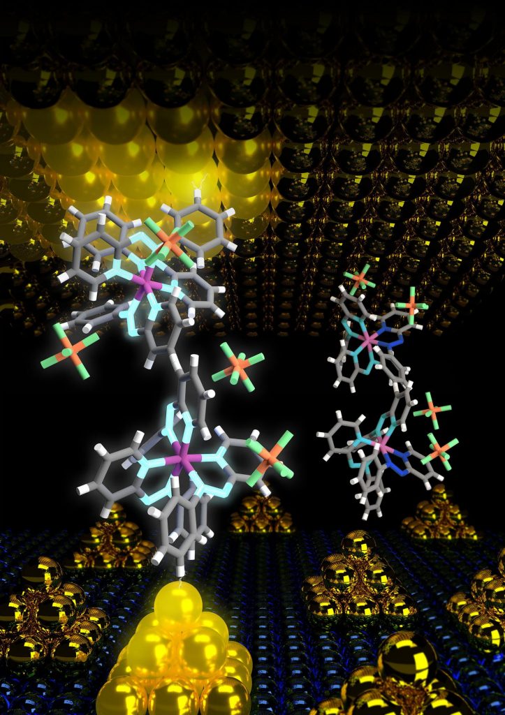
Artificial Neural Network (ANN) is a type of information processing system based on mimicking the principles of biological brains, and has been broadly applied in application domains such as pattern recognition, automatic control, signal processing, decision support system and artificial intelligence. Spiking Neural Network (SNN) is a type of biologically-inspired ANN that perform information processing based on discrete-time spikes. It is more biologically realistic than classic ANNs, and can potentially achieve much better performance-power ratio. Recently, researchers from Zhejiang University and Hangzhou Dianzi University in Hangzhou, China successfully developed the Darwin Neural Processing Unit (NPU), a neuromorphic hardware co-processor based on Spiking Neural Networks, fabricated by standard CMOS technology.
With the rapid development of the Internet-of-Things and intelligent hardware systems, a variety of intelligent devices are pervasive in today’s society, providing many services and convenience to people’s lives, but they also raise challenges of running complex intelligent algorithms on small devices. Sponsored by the college of Computer science of Zhejiang University, the research group led by Dr. De Ma from Hangzhou Dianzi university and Dr. Xiaolei Zhu from Zhejiang university has developed a co-processor named as Darwin.The Darwin NPU aims to provide hardware acceleration of intelligent algorithms, with target application domain of resource-constrained, low-power small embeddeddevices. It has been fabricated by 180nm standard CMOS process, supporting a maximum of 2048 neurons, more than 4 million synapses and 15 different possible synaptic delays. It is highly configurable, supporting reconfiguration of SNN topology and many parameters of neurons and synapses.Figure 1 shows photos of the die and the prototype development board, which supports input/output in the form of neural spike trains via USB port.
The successful development ofDarwin demonstrates the feasibility of real-time execution of Spiking Neural Networks in resource-constrained embedded systems. It supports flexible configuration of a multitude of parameters of the neural network, hence it can be used to implement different functionalities as configured by the user. Its potential applications include intelligent hardware systems, robotics, brain-computer interfaces, and others.Since it uses spikes for information processing and transmission,similar to biological neural networks, it may be suitable for analysis and processing of biological spiking neural signals, and building brain-computer interface systems by interfacing with animal or human brains. As a prototype application in Brain-Computer Interfaces, Figure 2 [not included here] describes an application example ofrecognizingthe user’s motor imagery intention via real-time decoding of EEG signals, i.e., whether he is thinking of left or right, and using it to control the movement direction of a basketball in the virtual environment. Different from conventional EEG signal analysis algorithms, the input and output to Darwin are both neural spikes: the input is spike trains that encode EEG signals; after processing by the neural network, the output neuron with the highest firing rate is chosen as the classification result.
The second generation of the Darwin Neural Processing Unit (Darwin NPU 2) as well as its corresponding toolchain and micro-operating system was released in Hangzhou recently. This research was led by Zhejiang University, with Hangzhou Dianzi University and Huawei Central Research Institute participating in the development and algorisms of the chip. The Darwin NPU 2 can be primarily applied to smart Internet of Things (IoT). It can support up to 150,000 neurons and has achieved the largest-scale neurons on a nationwide basis.
The Darwin NPU 2 is fabricated by standard 55nm CMOS technology. Every “neuromorphic” chip is made up of 576 kernels, each of which can support 256 neurons. It contains over 10 million synapses which can construct a powerful brain-inspired computing system.
“A brain-inspired chip can work like the neurons inside a human brain and it is remarkably unique in image recognition, visual and audio comprehension and naturalistic language processing,” said MA De, an associate professor at the College of Computer Science and Technology on the research team.
“In comparison with traditional chips, brain-inspired chips are more adept at processing ambiguous data, say, perception tasks. Another prominent advantage is their low energy consumption. In the process of information transmission, only those neurons that receive and process spikes will be activated while other neurons will stay dormant. In this case, energy consumption can be extremely low,” said Dr. ZHU Xiaolei at the School of Microelectronics.
To cater to the demands for voice business, Huawei Central Research Institute designed an efficient spiking neural network algorithm in accordance with the defining feature of the Darwin NPU 2 architecture, thereby increasing computing speeds and improving recognition accuracy tremendously.
Scientists have developed a host of applications, including gesture recognition, image recognition, voice recognition and decoding of electroencephalogram (EEG) signals, on the Darwin NPU 2 and reduced energy consumption by at least two orders of magnitude.
In comparison with the first generation of the Darwin NPU which was developed in 2015, the Darwin NPU 2 has escalated the number of neurons by two orders of magnitude from 2048 neurons and augmented the flexibility and plasticity of the chip configuration, thus expanding the potential for applications appreciably. The improvement in the brain-inspired chip will bring in its wake the revolution of computer technology and artificial intelligence. At present, the brain-inspired chip adopts a relatively simplified neuron model, but neurons in a real brain are far more sophisticated and many biological mechanisms have yet to be explored by neuroscientists and biologists. It is expected that in the not-too-distant future, a fascinating improvement on the Darwin NPU 2 will come over the horizon.
I haven’t been able to find a recent (i.e., post 2017) research paper featuring Darwin but there is another chip and research on that one was published in July 2019. First, the news.
The Tianjic chip
A July 31, 2019 article in the New York Times by Cade Metz describes the research and offers what seems to be a jaundiced perspective about the field of neuromorphic computing (Note: A link has been removed),
As corporate giants like Ford, G.M. and Waymo struggle to get their self-driving cars on the road, a team of researchers in China is rethinking autonomous transportation using a souped-up bicycle.
This bike can roll over a bump on its own, staying perfectly upright. When the man walking just behind it says “left,” it turns left, angling back in the direction it came.
It also has eyes: It can follow someone jogging several yards ahead, turning each time the person turns. And if it encounters an obstacle, it can swerve to the side, keeping its balance and continuing its pursuit.
… Chinese researchers who built the bike believe it demonstrates the future of computer hardware. It navigates the world with help from what is called a neuromorphic chip, modeled after the human brain.
Here’s a video, released by the researchers, demonstrating the chip’s abilities,
The short video did not show the limitations of the bicycle (which presumably tips over occasionally), and even the researchers who built the bike admitted in an email to The Times that the skills on display could be duplicated with existing computer hardware. But in handling all these skills with a neuromorphic processor, the project highlighted the wider effort to achieve new levels of artificial intelligence with novel kinds of chips.
This effort spans myriad start-up companies and academic labs, as well as big-name tech companies like Google, Intel and IBM. And as the Nature paper demonstrates, the movement is gaining significant momentum in China, a country with little experience designing its own computer processors, but which has invested heavily in the idea of an “A.I. chip.”
…
If you can get past what seems to be a patronizing attitude, there are some good explanations and cogent criticisms in the piece (Metz’s July 31, 2019 article, Note: Links have been removed),
… it faces significant limitations.
A neural network doesn’t really learn on the fly. Engineers train a neural network for a particular task before sending it out into the real world, and it can’t learn without enormous numbers of examples. OpenAI, a San Francisco artificial intelligence lab, recently built a system that could beat the world’s best players at a complex video game called Dota 2. But the system first spent months playing the game against itself, burning through millions of dollars in computing power.
Researchers aim to build systems that can learn skills in a manner similar to the way people do. And that could require new kinds of computer hardware. Dozens of companies and academic labs are now developing chips specifically for training and operating A.I. systems. The most ambitious projects are the neuromorphic processors, including the Tianjic chip under development at Tsinghua University in China.
Such chips are designed to imitate the network of neurons in the brain, not unlike a neural network but with even greater fidelity, at least in theory.
Neuromorphic chips typically include hundreds of thousands of faux neurons, and rather than just processing 1s and 0s, these neurons operate by trading tiny bursts of electrical signals, “firing” or “spiking” only when input signals reach critical thresholds, as biological neurons do.
…
Tiernan Ray’s August 3, 2019 article about the chip for ZDNet.com offers some thoughtful criticism with a side dish of snark (Note: Links have been removed),
Nature magazine’s cover story [July 31, 2019] is about a Chinese chip [Tianjic chip]that can run traditional deep learning code and also perform “neuromorophic” operations in the same circuitry. The work’s value seems obscured by a lot of hype about “artificial general intelligence” that has no real justification.
The term “artificial general intelligence,” or AGI, doesn’t actually refer to anything, at this point, it is merely a placeholder, a kind of Rorschach Test for people to fill the void with whatever notions they have of what it would mean for a machine to “think” like a person.
Despite that fact, or perhaps because of it, AGI is an ideal marketing term to attach to a lot of efforts in machine learning. Case in point, a research paper featured on the cover of this week’s Nature magazine about a new kind of computer chip developed by researchers at China’s Tsinghua University that could “accelerate the development of AGI,” they claim.
The chip is a strange hybrid of approaches, and is intriguing, but the work leaves unanswered many questions about how it’s made, and how it achieves what researchers claim of it. And some longtime chip observers doubt the impact will be as great as suggested.
“This paper is an example of the good work that China is doing in AI,” says Linley Gwennap, longtime chip-industry observer and principal analyst with chip analysis firm The Linley Group. “But this particular idea isn’t going to take over the world.”
The premise of the paper, “Towards artificial general intelligence with hybrid Tianjic chip architecture,” is that to achieve AGI, computer chips need to change. That’s an idea supported by fervent activity these days in the land of computer chips, with lots of new chip designs being proposed specifically for machine learning.
The Tsinghua authors specifically propose that the mainstream machine learning of today needs to be merged in the same chip with what’s called “neuromorphic computing.” Neuromorphic computing, first conceived by Caltech professor Carver Mead in the early ’80s, has been an obsession for firms including IBM for years, with little practical result.
…
[Missing details about the chip] … For example, the part is said to have “reconfigurable” circuits, but how the circuits are to be reconfigured is never specified. It could be so-called “field programmable gate array,” or FPGA, technology or something else. Code for the project is not provided by the authors as it often is for such research; the authors offer to provide the code “on reasonable request.”
More important is the fact the chip may have a hard time stacking up to a lot of competing chips out there, says analyst Gwennap. …
…
What the paper calls ANN and SNN are two very different means of solving similar problems, kind of like rotating (helicopter) and fixed wing (airplane) are for aviation,” says Gwennap. “Ultimately, I expect ANN [?] and SNN [spiking neural network] to serve different end applications, but I don’t see a need to combine them in a single chip; you just end up with a chip that is OK for two things but not great for anything.”
But you also end up generating a lot of buzz, and given the tension between the U.S. and China over all things tech, and especially A.I., the notion China is stealing a march on the U.S. in artificial general intelligence — whatever that may be — is a summer sizzler of a headline.
ANN could be either artificial neural network or something mentioned earlier in Ray’s article, a shortened version of CANN [continuous attractor neural network].
Shelly Fan’s August 7, 2019 article for the SingularityHub is almost as enthusiastic about the work as the podcasters for Nature magazine were (a little more about that later),
The study shows that China is readily nipping at the heels of Google, Facebook, NVIDIA, and other tech behemoths investing in developing new AI chip designs—hell, with billions in government investment it may have already had a head start. A sweeping AI plan from 2017 looks to catch up with the US on AI technology and application by 2020. By 2030, China’s aiming to be the global leader—and a champion for building general AI that matches humans in intellectual competence.
The country’s ambition is reflected in the team’s parting words.
“Our study is expected to stimulate AGI [artificial general intelligence] development by paving the way to more generalized hardware platforms,” said the authors, led by Dr. Luping Shi at Tsinghua University.
…
Using nanoscale fabrication, the team arranged 156 FCores, containing roughly 40,000 neurons and 10 million synapses, onto a chip less than a fifth of an inch in length and width. Initial tests showcased the chip’s versatility, in that it can run both SNNs and deep learning algorithms such as the popular convolutional neural network (CNNs) often used in machine vision.
Compared to IBM TrueNorth, the density of Tianjic’s cores increased by 20 percent, speeding up performance ten times and increasing bandwidth at least 100-fold, the team said. When pitted against GPUs, the current hardware darling of machine learning, the chip increased processing throughput up to 100 times, while using just a sliver (1/10,000) of energy.
Shelly Xuelai Fan is a neuroscientist-turned-science writer. She completed her PhD in neuroscience at the University of British Columbia, where she developed novel treatments for neurodegeneration. While studying biological brains, she became fascinated with AI and all things biotech. Following graduation, she moved to UCSF [University of California at San Francisco] to study blood-based factors that rejuvenate aged brains. She is the co-founder of Vantastic Media, a media venture that explores science stories through text and video, and runs the award-winning blog NeuroFantastic.com. Her first book, “Will AI Replace Us?” (Thames & Hudson) will be out April 2019.
Onto Nature. Here’s a link to and a citation for the paper,
Towards artificial general intelligence with hybrid Tianjic chip architecture by Jing Pei, Lei Deng, Sen Song, Mingguo Zhao, Youhui Zhang, Shuang Wu, Guanrui Wang, Zhe Zou, Zhenzhi Wu, Wei He, Feng Chen, Ning Deng, Si Wu, Yu Wang, Yujie Wu, Zheyu Yang, Cheng Ma, Guoqi Li, Wentao Han, Huanglong Li, Huaqiang Wu, Rong Zhao, Yuan Xie & Luping Shi. Nature volume 572, pages106–111(2019) DOI: https//doi.org/10.1038/s41586-019-1424-8 Published: 31 July 2019 Issue Date: 01 August 2019
This paper is behind a paywall.
The July 31, 2019 Nature podcast, which includes a segment about the Tianjic chip research from China, which is at the 9 mins. 13 secs. mark (AI hardware) or you can scroll down about 55% of the way to the transcript of the interview with Luke Fleet, the Nature editor who dealt with the paper.
Some thoughts
The pundits put me in mind of my own reaction when I heard about phones that could take pictures. I didn’t see the point but, as it turned out, there was a perfectly good reason for combining what had been two separate activities into one device. It was no longer just a telephone and I had completely missed the point.
This too may be the case with the Tianjic chip. I think it’s too early to say whether or not it represents a new type of chip or if it’s a dead end.
I went down a rabbit hole while trying to figure out the difference between ‘organic’ memristors and standard memristors. I have put the results of my investigation at the end of this post. First, there’s the news.
An April 21, 2020 news item on ScienceDaily explains why researchers are so focused on memristors and brainlike computing,
The advent of artificial intelligence, machine learning and the internet of things is expected to change modern electronics and bring forth the fourth Industrial Revolution. The pressing question for many researchers is how to handle this technological revolution.
“It is important for us to understand that the computing platforms of today will not be able to sustain at-scale implementations of AI algorithms on massive datasets,” said Thirumalai Venkatesan, one of the authors of a paper published in Applied Physics Reviews, from AIP Publishing.
“Today’s computing is way too energy-intensive to handle big data. We need to rethink our approaches to computation on all levels: materials, devices and architecture that can enable ultralow energy computing.”
Brain-inspired electronics with organic memristors could offer a functionally promising and cost- effective platform, according to Venkatesan. Memristive devices are electronic devices with an inherent memory that are capable of both storing data and performing computation. Since memristors are functionally analogous to the operation of neurons, the computing units in the brain, they are optimal candidates for brain-inspired computing platforms.
Until now, oxides have been the leading candidate as the optimum material for memristors. Different material systems have been proposed but none have been successful so far.
“Over the last 20 years, there have been several attempts to come up with organic memristors, but none of those have shown any promise,” said Sreetosh Goswami, lead author on the paper. “The primary reason behind this failure is their lack of stability, reproducibility and ambiguity in mechanistic understanding. At a device level, we are now able to solve most of these problems,”
This new generation of organic memristors is developed based on metal azo complex devices, which are the brainchild of Sreebata Goswami, a professor at the Indian Association for the Cultivation of Science in Kolkata and another author on the paper.
“In thin films, the molecules are so robust and stable that these devices can eventually be the right choice for many wearable and implantable technologies or a body net, because these could be bendable and stretchable,” said Sreebata Goswami. A body net is a series of wireless sensors that stick to the skin and track health.
The next challenge will be to produce these organic memristors at scale, said Venkatesan.
“Now we are making individual devices in the laboratory. We need to make circuits for large-scale functional implementation of these devices.”
Caption: The device structure at a molecular level. The gold nanoparticles on the bottom electrode enhance the field enabling an ultra-low energy operation of the molecular device. Credit Sreetosh Goswami, Sreebrata Goswami and Thirumalai Venky Venkatesan
This undated article on Nanowerk provides a relatively complete and technical description of memristors in general (Note: A link has been removed),
A memristor (named as a portmanteau of memory and resistor) is a non-volatile electronic memory device that was first theorized by Leon Ong Chua in 1971 as the fourth fundamental two-terminal circuit element following the resistor, the capacitor, and the inductor (IEEE Transactions on Circuit Theory, “Memristor-The missing circuit element”).
Its special property is that its resistance can be programmed (resistor function) and subsequently remains stored (memory function). Unlike other memories that exist today in modern electronics, memristors are stable and remember their state even if the device loses power.
However, it was only almost 40 years later that the first practical device was fabricated. This was in 2008, when a group led by Stanley Williams at HP Research Labs realized that switching of the resistance between a conducting and less conducting state in metal-oxide thin-film devices was showing Leon Chua’s memristor behavior. …
The article on Nanowerk includes an embedded video presentation on memristors given by Stanley Williams (also known as R. Stanley Williams).
The memristor is composed of the transition metal ruthenium complexed with “azo-aromatic ligands.” [emphasis mine] The theoretical work enabling this material was performed at Yale, and the organic molecules were synthesized at the Indian Association for the Cultivation of Sciences. …
I highlighted ‘ligands’ because that appears to be the difference. However, there is more than one type of ligand on Wikipedia.
In coordination chemistry, a ligand[help 1] is an ion or molecule (functional group) that binds to a central metal atom to form a coordination complex …
Ligand, an atom, ion, or functional group that donates one or more of its electrons through a coordinate covalent bond to one or more central atoms or ions
Ligand (biochemistry), a substance that binds to a protein
a ‘guest’ in host–guest chemistry
I did take a look at the paper and did not see any references to proteins or other biomolecules that I could recognize as such. I’m not sure why the researchers are describing their device as an ‘organic’ memristor but this may reflect a shortcoming in the definitions I have found or shortcomings in my reading of the paper rather than an error on their parts.
Hopefully, more research will be forthcoming and it will be possible to better understand the terminology.
Almost daily, new technologies are being developed to help innovate the way people give or the way organizations offer opportunities to advance their causes. There is no going back.
The charitable sector – along with society at large – is now fully in the midst of what is being called the Fourth Industrial Revolution, a term first brought to prominence among CEOs, thought leaders and policy makers at the 2016 World Economic Forum. And if you haven’t heard the phrase yet, get ready to hear it tons more as economies around the world embrace it.
To be clear, the Fourth Industrial Revolution is the newest disruption in the way our world works. When you hear someone talk about it, what they’re describing is the massive technological shift in our business and personal ecosystems that now rely heavily on things like artificial intelligence, quantum computing, 3D printing and the general “Internet of things.”
…
Still, now more than ever, charitable business is getting done and being advanced by sector pioneers who aren’t afraid to make use of new technologies on offer to help civil society.
…
It seems like everywhere one turns, the topic of artificial intelligence (A.I.) is increasingly becoming subject of choice.
This is no different in the charitable sector, and particularly so for a new company called Fundraise Wisely (aka Wisely). Its co-founder and CEO, Artiom Komarov, explains a bit about what exactly his tech is doing for the sector.
“We help accelerate fundraising, with A.I. At a product level, we connect to your CRM (content relationship management system) and predict the next gift and next gift date for every donor. We then use that information to help you populate and prioritize donor portfolios,” Komarov states.
He notes that his company is seeing increased demand for innovative technologies from charities over the last while.
“What we’re hearing is that… A.I. tech is compelling because at the end of the day it’s meant to move the bottom line, helping nonprofits grow their revenue. We’ve also found that internally [at a charitable organization] there’s always a champion that sees the potential impact of technology; and that’s a great place to start with change,” Komarov says. “If it’s done right, tech can be an enabler of better work for organizations. From both research and experience, we know that tech adoption usually fails because of culture rather than the underlying technology. We’re here to work with the client closely to help that transition.”
…
I would like to have seen some numbers. For example, Komarov says that AI is having a positive impact on a charity’s bottom line. So, how much money did one of these charities raise? Was it more money than they would have made without AI? Assuming they did manage to raise greater funds, could another technology been more cost effective?
At the beginning of this year the [UK] Cabinet Office and Nesta [formerly National Endowment for Science, Technology and the Arts {NESTA}] announced a £10m fund to invest in innovation in giving. The first tranche of this money has already been invested in promising initiatives such as Timto which allows you to create a gift list that includes a charity donation and Pennies, whose electronic money box allows customers to donate when paying for something in a shop using a credit card. Small and sizeable organisations alike are now using web and mobile technologies to make giving more convenient, more social and more compelling.
…
Butt’s and Shah’s focus was on mobile technologies and social networks. Like Levy-Ajzenkopf’s article, there’s no discussion of any possible downside to these technologies, e.g., privacy issues. As well, the inevitability of this move toward more technology for charity is explicitly stated by Levy-Ajzenkopf “There is no going back” and noted less starkly by Butt and Shah “… innovation is becoming increasingly important for the success of charities.” To rephrase my concern, are we utilizing technology in our work or are we serving the needs of our technology?
Finally, for anyone who’s curious about the Fourth Industrial Revolution, I have a December 3, 2015 posting about it.
Purdue University researchers have developed a new fabric innovation that allows the wearer to control electronic devices through the clothing. Courtesy: Purdue University
I like the image but do they really want someone pressing a cufflink? Anyway, being able to turn on your house lights and music system with your clothing would certainly be convenient. From an August 8, 2019 Purdue University (Indiana, US) news release (also on EurekAlert) by Chris Adam,
A new addition to your wardrobe may soon help you turn on the lights and music – while also keeping you fresh, dry, fashionable, clean and safe from the latest virus that’s going around.
Purdue University researchers have developed a new fabric innovation that allows wearers to control electronic devices through clothing.
“It is the first time there is a technique capable to transform any existing cloth item or textile into a self-powered e-textile containing sensors, music players or simple illumination displays using simple embroidery without the need for expensive fabrication processes requiring complex steps or expensive equipment,” said Ramses Martinez, an assistant professor in the School of Industrial Engineering and in the Weldon School of Biomedical Engineering in Purdue’s College of Engineering.
The technology is featured in the July 25 [2019] edition of Advanced Functional Materials.
“For the first time, it is possible to fabricate textiles that can protect you from rain, stains, and bacteria while they harvest the energy of the user to power textile-based electronics,” Martinez said. “These self-powered e-textiles also constitute an important advancement in the development of wearable machine-human interfaces, which now can be washed many times in a conventional washing machine without apparent degradation.
Martinez said the Purdue waterproof, breathable and antibacterial self-powered clothing is based on omniphobic triboelectric nanogeneragtors (RF-TENGs) – which use simple embroidery and fluorinated molecules to embed small electronic components and turn a piece of clothing into a mechanism for powering devices. The Purdue team says the RF-TENG technology is like having a wearable remote control that also keeps odors, rain, stains and bacteria away from the user.
“While fashion has evolved significantly during the last centuries and has easily adopted recently developed high-performance materials, there are very few examples of clothes on the market that interact with the user,” Martinez said. “Having an interface with a machine that we are constantly wearing sounds like the most convenient approach for a seamless communication with machines and the Internet of Things.”
The technology is being patented through the Purdue Research Foundation Office of Technology Commercialization. The researchers are looking for partners to test and commercialize their technology.
Their work aligns with Purdue’s Giant Leaps celebration of the university’s global advancements in artificial intelligence and health as part of Purdue’s 150th anniversary. It is one of the four themes of the yearlong celebration’s Ideas Festival, designed to showcase Purdue as an intellectual center solving real-world issues.
A July 19, 2019 news item on phys.org describes research that may result in a substantive change for information technology,
A team of researchers from Tokyo Institute of Technology has gained unprecedented insight into the inner workings of an atomic switch. By investigating the composition of the tiny metal ‘bridge’ that forms inside the switch, their findings may spur the design of atomic switches with improved performance.
Atomic switches are hailed as the tiniest of electrochemical switches that could change the face of information technology. Due to their nanoscale dimensions and low power consumption, they hold promise for integration into next-generation circuits that could drive the development of artificial intelligence (AI) and Internet of Things (IoT) devices.
Although various designs have emerged, one intriguing question concerns the nature of the metallic filament, or bridge, that is key to the operation of the switch. The bridge forms inside a metal sulfide layer sandwiched between two electrodes [see figure below], and is controlled by applying a voltage that induces an electrochemical reaction. The formation and annihilation of this bridge determines whether the switch is on or off.
Now, a research group including Akira Aiba and Manabu Kiguchi and colleagues at Tokyo Institute of Technology’s Department of Chemistry has found a useful way to examine precisely what the bridge is composed of.
By cooling the atomic switch enough so as to be able to investigate the bridge using a low-temperature measurement technique called point contact spectroscopy (PCS) [2], their study revealed that the bridge is made up of metal atoms from both the electrode and the metal sulfide layer. This surprising finding controverts the prevailing notion that the bridge derives from the electrode only, Kiguchi explains.
The team compared atomic switches with different combinations of electrodes (Pt and Ag, or Pt and Cu) and metal sulfide layers (Cu2S and Ag2S). In both cases, they found that the bridge is mainly composed of Ag.
The reason behind the dominance of Ag in the bridge is likely due to “the higher mobility of Ag ions compared to Cu ions”, the researchers say in their paper published in ACS Applied Materials & Interfaces.
They conclude that “it would be better to use metals with low mobility” for designing atomic switches with higher stability.
Much remains to be explored in the advancement of atomic switch technologies, and the team is continuing to investigate which combination of elements would be the most effective in improving performance.
###
Technical terms [1] Atomic switch: The idea behind an atomic switch — one that can be controlled by the motion of a single atom — was introduced by Donald Eigler and colleagues at the IBM Almaden Research Center in 1991. Interest has since focused on how to realize and harness the potential of such extremely small switches for use in logic circuits and memory devices. Over the past two decades, researchers in Japan have taken a world-leading role in the development of atomic switch technologies. [2] Point contact spectroscopy: A method of measuring the properties or excitations of single atoms at low temperature.
Caption: The ‘bridge’ that forms within the metal sulfide layer, connecting two metal electrodes, results in the atomic switch being turned on. Credit: Manabu Kiguchi
For anyone who might need a bit of a refresher for the chemical elements, Pt is platinum, Ag is silver, and Cu is copper. So, with regard to the metal sulfide layers Cu2S is copper sulfide and Ag2S is silver sulfide.
This research is from Purdue University (Indiana, US) and the University of Virginia (US) increases and improves the interactivity between objects in what’s called the Internet of Things (IoT).
Caption: Electronic stickers can turn ordinary toy blocks into high-tech sensors within the ‘internet of things.’ Credit: Purdue University image/Chi Hwan Lee
Billions of objects ranging from smartphones and watches to buildings, machine parts and medical devices have become wireless sensors of their environments, expanding a network called the “internet of things.”
As society moves toward connecting all objects to the internet — even furniture and office supplies — the technology that enables these objects to communicate and sense each other will need to scale up.
Researchers at Purdue University and the University of Virginia have developed a new fabrication method that makes tiny, thin-film electronic circuits peelable from a surface. The technique not only eliminates several manufacturing steps and the associated costs, but also allows any object to sense its environment or be controlled through the application of a high-tech sticker.
Eventually, these stickers could also facilitate wireless communication. …
“We could customize a sensor, stick it onto a drone, and send the drone to dangerous areas to detect gas leaks, for example,” said Chi Hwan Lee, Purdue assistant professor of biomedical engineering and mechanical engineering.
Most of today’s electronic circuits are individually built on their own silicon “wafer,” a flat and rigid substrate. The silicon wafer can then withstand the high temperatures and chemical etching that are used to remove the circuits from the wafer.
But high temperatures and etching damage the silicon wafer, forcing the manufacturing process to accommodate an entirely new wafer each time.
Lee’s new fabrication technique, called “transfer printing,” cuts down manufacturing costs by using a single wafer to build a nearly infinite number of thin films holding electronic circuits. Instead of high temperatures and chemicals, the film can peel off at room temperature with the energy-saving help of simply water.
“It’s like the red paint on San Francisco’s Golden Gate Bridge – paint peels because the environment is very wet,” Lee said. “So in our case, submerging the wafer and completed circuit in water significantly reduces the mechanical peeling stress and is environmentally-friendly.”
A ductile metal layer, such as nickel, inserted between the electronic film and the silicon wafer, makes the peeling possible in water. These thin-film electronics can then be trimmed and pasted onto any surface, granting that object electronic features.
Putting one of the stickers on a flower pot, for example, made that flower pot capable of sensing temperature changes that could affect the plant’s growth.
Lee’s lab also demonstrated that the components of electronic integrated circuits work just as well before and after they were made into a thin film peeled from a silicon wafer. The researchers used one film to turn on and off an LED light display.
“We’ve optimized this process so that we can delaminate electronic films from wafers in a defect-free manner,” Lee said.
This technology holds a non-provisional U.S. patent. The work was supported by the Purdue Research Foundation, the Air Force Research Laboratory (AFRL-S-114-054-002), the National Science Foundation (NSF-CMMI-1728149) and the University of Virginia.
Dexter Johnson provides some context in his July 25, 2018 posting on the Nanoclast blog (on the IEEE [Institute of Electronic and Electrical Engineers] website), Note: A link has been removed,
The Internet of Things (IoT), the interconnection of billions of objects and devices that will be communicating with each other, has been the topic of many futurists’ projections. However, getting the engineering sorted out with the aim of fully realizing the myriad visions for IoT is another story. One key issue to address: How do you get the electronics onto these devices efficiently and economically?
A team of researchers from Purdue University and the University of Virginia has developed a new manufacturing process that could make equipping a device with all the sensors and other electronics that will make it Internet capable as easily as putting a piece of tape on it.
…
… this new approach makes use of a water environment at room temperature to control the interfacial debonding process. This allows clean, intact delamination of prefabricated thin film devices when they’re pulled away from the original wafer.
The use of mechanical peeling in water rather than etching solution provides a number of benefits in the manufacturing scheme. Among them are simplicity, controllability, and cost effectiveness, says Chi Hwan Lee, assistant professor at Purdue University and coauthor of the paper chronicling the research.
If you have the time, do read Dexter’s piece. He always adds something that seems obvious in retrospect but wasn’t until he wrote it.
The conference itself will be held from May 22 – 24, 2019 at Arizona State University (ASU) and the deadline for abstracts is January 31, 2019. Here’s the news straight from the January 8, 2019 email announcement,
The Seventh Annual Conference on Governance of Emerging Technologies & Science (GETS)
May 22-24, 2019 / ASU / Sandra Day O’Connor College of Law 111 E. Taylor St., Phoenix, AZ The conference will consist of plenary and session presentations and discussions on regulatory, governance, legal, policy, social and ethical aspects of emerging technologies, including nanotechnology, synthetic biology, gene editing, biotechnology, genomics, personalized medicine, digital health, human enhancement, artificial intelligence, virtual reality, internet of things (IoT), blockchain and much, much more! Submit Your Abstract Here: 2019 Abstract or Conference Website
Call for abstracts:
The co-sponsors invite submission of abstracts for proposed presentations. Submitters of abstracts need not provide a written paper, although provision will be made for posting and possible post-conference publication of papers for those who are interested. Abstracts are invited for any aspect or topic relating to the governance of emerging technologies, including any of the technologies listed above.
· Abstracts should not exceed 500 words and must contain your name and email address. · Abstracts must be submitted by January 31, 2019 to be considered. · The sponsors will pay for the conference registration (including all conference meals and events) for one presenter for each accepted abstract. In addition, we will have limited funds available for travel subsidies (application included in submission form). For more informationcontact our Executive Director Josh Abbott at Josh.Abbott@asu.edu.
I’m a little late with this but there’s still time to register should you happen to be in or able to get to Dubai easily. From an October 18, 2018 International Telecommunication Union (ITU) Media Advisory (received via email),
Media registration is open for the 2018 ITU Plenipotentiary Conference (PP-18) – the highest policy-making body of the International Telecommunication Union (ITU), the United Nations’ specialized agency for information and communication technology. This will be closing soon, so all media intending to attend the event MUST register as soon as possible here.
Held every four years, it is the key event at which ITU’s 193 Member States decide on the future role of the organization, thereby determining ITU’s ability to influence and affect the development of information and communication technologies (ICTs) worldwide. It is expected to attract around 3,000 participants, including Heads of State and an estimated 130 VIPs from more than 193 Member States and more than 800 private companies, academic institutions and national, regional and international bodies.
ITU plays an integral role in enabling the development and implementation of ICTs worldwide through its mandate to: coordinate the shared global use of the radio spectrum, promote international cooperation in assigning satellite orbits, work to improve communication infrastructure in the developing world, and establish worldwide standards that foster seamless interconnection of a vast range of communications systems.
Delegates will tackle a number of pressing issues, from strategies to promote digital inclusion and bridge the digital divide, to ways to leverage such emerging technologies as the Internet of Things, Artificial Intelligence, 5G, and others, to improve the way all of us, everywhere, live and work.
The conference also sets ITU’s Financial Plan and elects its five top executives – Secretary-General, Deputy Secretary-General, and the Directors of the Radiocommunication, Telecommunication Standardization and Telecommunication Development Bureaux – who will guide its work over the next four years.
What: ITU Plenipotentiary Conference 2018 (PP-18) sets the next four-year strategy, budget and leadership of ITU.
Why: Finance, Business, Tech, Development and Foreign Affairs reporters will find PP-18 relevant to their newsgathering. Decisions made at PP-18 are designed to create an enabling ICT environment where the benefits of digital connectivity can reach all people and economies, everywhere. As such, these decisions can have an impact on the telecommunication and technology sectors as well as developed and developing countries alike.
When: 29 October – 16 November 2018: With several Press Conferences planned during the event.
* Historically the Opening, Closing and Plenary sessions of this conference are open to media. Confirmation of those sessions open to media, and Press Conference times, will be made closer to the event date.
Where: Dubai World Trade Center, Dubai, United Arab Emirates
More Information:
Media registration is required to participate in this event. To meet security protocols, there is strictly no admittance to the venue without an event badge.
1. Journalists* should provide an official letter of assignment from the Editor-in-Chief (or the News Editor for radio/TV). One letter per crew/editorial team will suffice. Editors-in-Chief and Bureau Chiefs should submit a letter from their Director. Please email this to pressreg@itu.int, along with the required supporting credentials below:
print and online publications should be available to the general public and published at least 6 times a year by an organization whose principle business activity is publishing and which generally carries paid advertising;
o 2 copies of recent byline articles published within the last 4 months.
news wire services should provide news coverage to subscribers, including newspapers, periodicals and/or television networks;
o 2 copies of recent byline articles or broadcasting material published within the last 4 months.
broadcast should provide news and information programmes to the general public. Independent film and video production companies can only be accredited if officially mandated by a broadcast station via a letter of assignment;
o broadcasting material published within the last 4 months.
freelance journalists including photographers, must provide clear documentation that they are on assignment from a specific news organization or publication. Evidence that they regularly supply journalistic content to recognized media may be acceptable in the absence of an assignment letter at the discretion of the ITU Media Relations Service.
o a valid assignment letter from the news organization or publication.
2. Bloggers may be granted accreditation if blog content is deemed relevant to the industry, contains news commentary, is regularly updated and made publicly available. Corporate bloggers are invited to register as participants. Please see Guidelines for Blogger Accreditation below for more details.
Guidelines for Blogger Accreditation
ITU is committed to working with independent ‘new media’ reporters and columnists who reach their audiences via blogs, podcasts, video blogs and other online media. These are the guidelines we use to determine whether to issue official media accreditation to independent online media representatives:
ITU reserves the right to request traffic data from a third party (Sitemeter, Technorati, Feedburner, iTunes or equivalent) when considering your application. While the decision to grant access is not based solely on traffic/subscriber data, we ask that applicants provide sufficient transparency into their operations to help us make a fair and timely decision.
Obtaining media accreditation for ITU events is an opportunity to meet and interact with key industry and political figures. While continued accreditation for ITU events is not directly contingent on producing coverage, owing to space limitations we may take this into consideration when processing future accreditation requests. Following any ITU event for which you are accredited, we therefore kindly request that you forward a link to your post/podcast/video blog to pressreg@itu.int.
Bloggers who are granted access to ITU events are expected to act professionally. Those who do not maintain the standards expected of professional media representatives run the risk of having their accreditation withdrawn.