Tag Archives: neuromorphic computing

Butterfly mating inspires neuromorphic (brainlike) computing

Michael Berger writes about a multisensory approach to neuromorphic computing inspired by butterflies in his February 2, 2024 Nanowerk Spotlight article, Note: Links have been removed,

Artificial intelligence systems have historically struggled to integrate and interpret information from multiple senses the way animals intuitively do. Humans and other species rely on combining sight, sound, touch, taste and smell to better understand their surroundings and make decisions. However, the field of neuromorphic computing has largely focused on processing data from individual senses separately.

This unisensory approach stems in part from the lack of miniaturized hardware able to co-locate different sensing modules and enable in-sensor and near-sensor processing. Recent efforts have targeted fusing visual and tactile data. However, visuochemical integration, which merges visual and chemical information to emulate complex sensory processing such as that seen in nature—for instance, butterflies integrating visual signals with chemical cues for mating decisions—remains relatively unexplored. Smell can potentially alter visual perception, yet current AI leans heavily on visual inputs alone, missing a key aspect of biological cognition.

Now, researchers at Penn State University have developed bio-inspired hardware that embraces heterogeneous integration of nanomaterials to allow the co-location of chemical and visual sensors along with computing elements. This facilitates efficient visuochemical information processing and decision-making, taking cues from the courtship behaviors of a species of tropical butterfly.

In the paper published in Advanced Materials (“A Butterfly-Inspired Multisensory Neuromorphic Platform for Integration of Visual and Chemical Cues”), the researchers describe creating their visuochemical integration platform inspired by Heliconius butterflies. During mating, female butterflies rely on integrating visual signals like wing color from males along with chemical pheromones to select partners. Specialized neurons combine these visual and chemical cues to enable informed mate choice.

To emulate this capability, the team constructed hardware encompassing monolayer molybdenum disulfide (MoS2) memtransistors serving as visual capture and processing components. Meanwhile, graphene chemitransistors functioned as artificial olfactory receptors. Together, these nanomaterials provided the sensing, memory and computing elements necessary for visuochemical integration in a compact architecture.

While mating butterflies served as inspiration, the developed technology has much wider relevance. It represents a significant step toward overcoming the reliance of artificial intelligence on single data modalities. Enabling integration of multiple senses can greatly improve situational understanding and decision-making for autonomous robots, vehicles, monitoring devices and other systems interacting with complex environments.

The work also helps progress neuromorphic computing approaches seeking to emulate biological brains for next-generation ML acceleration, edge deployment and reduced power consumption. In nature, cross-modal learning underpins animals’ adaptable behavior and intelligence emerging from brains organizing sensory inputs into unified percepts. This research provides a blueprint for hardware co-locating sensors and processors to more closely replicate such capabilities

It’s fascinating to me how many times butterflies inspire science,

Butterfly-inspired visuo-chemical integration. a) A simplified abstraction of visual and chemical stimuli from male butterflies and visuo-chemical integration pathway in female butterflies. b) Butterfly-inspired neuromorphic hardware comprising of monolayer MoS2 memtransistor-based visual afferent neuron, graphene-based chemoreceptor neuron, and MoS2 memtransistor-based neuro-mimetic mating circuits. Courtesy: Wiley/Penn State University Researchers

Here’s a link to and a citation for the paper,

A Butterfly-Inspired Multisensory Neuromorphic Platform for Integration of Visual and Chemical Cues by Yikai Zheng, Subir Ghosh, Saptarshi Das. Advanced Materials SOI: https://doi.org/10.1002/adma.202307380 First published: 09 December 2023

This paper is open access.

Brain-inspired (neuromrophic) computing with twisted magnets and a patent for manufacturing permanent magnets without rare earths

I have two news bits both of them concerned with magnets.

Patent for magnets that can be made without rare earths

I’m starting with the patent news first since this is (as the company notes in its news release) a “Landmark Patent Issued for Technology Critically Needed to Combat Chinese Monopoly.”

For those who don’t know, China supplies most of the rare earths used in computers, smart phones, and other devices. On general principles, having a single supplier dominate production of and access to a necessary material for devices that most of us rely on can raise tensions. Plus, you can’t mine for resources forever.

This December 19, 2023 Nanocrystal Technology LP news release heralds an exciting development (for the impatient, further down the page I have highlighted the salient sections),

Nanotechnology Discovery by 2023 Nobel Prize Winner Became Launch Pad to Create Permanent Magnets without Rare Earths from China

NEW YORK, NY, UNITED STATES, December 19, 2023 /EINPresswire.com/ — Integrated Nano-Magnetics Corp, a wholly owned subsidiary of Nanocrystal Technology LP, was awarded a patent for technology built upon a fundamental nanoscience discovery made by Aleksey Yekimov, its former Chief Scientific Officer.

This patent will enable the creation of strong permanent magnets which are critically needed for both industrial and military applications but cannot be manufactured without certain “rare earth” elements available mostly from China.

At a glittering awards ceremony held in Stockholm on December10, 2023, three scientists, Aleksey Yekimov, Louis Brus (Professor at Columbia University) and Moungi Bawendi (Professor at MIT) were honored with the Nobel Prize in Chemistry for their discovery of the “quantum dot” which is now fueling practical applications in tuning the colors of LEDs, increasing the resolution of TV screens, and improving MRI imaging.

As stated by the Royal Swedish Academy of Sciences, “Quantum dots are … bringing the greatest benefits to humankind. Researchers believe that in the future they could contribute to flexible electronics, tiny sensors, thinner solar cells, and encrypted quantum communications – so we have just started exploring the potential of these tiny particles.”

Aleksey Yekimov worked for over 19 years until his retirement as Chief Scientific Officer of Nanocrystals Technology LP, an R & D company in New York founded by two Indian-American entrepreneurs, Rameshwar Bhargava and Rajan Pillai.

Yekimov, who was born in Russia, had already received the highest scientific honors for his work before he immigrated to USA in 1999. Yekimov was greatly intrigued by Nanocrystal Technology’s research project and chose to join the company as its Chief Scientific Officer.

During its early years, the company worked on efficient light generation by doping host nanoparticles about the same size as a quantum dot with an additional impurity atom. Bhargava came up with the novel idea of incorporating a single impurity atom, a dopant, into a quantum dot sized host, and thus achieve an extraordinary change in the host material’s properties such as inducing strong permanent magnetism in weak, readily available paramagnetic materials. To get a sense of the scale at which nanotechnology works, and as vividly illustrated by the Nobel Foundation, the difference in size between a quantum dot and a soccer ball is about the same as the difference between a soccer ball and planet Earth.

Currently, strong permanent magnets are manufactured from “rare earths” available mostly in China which has established a near monopoly on the supply of rare-earth based strong permanent magnets. Permanent magnets are a fundamental building block for electro-mechanical devices such as motors found in all automobiles including electric vehicles, trucks and tractors, military tanks, wind turbines, aircraft engines, missiles, etc. They are also required for the efficient functioning of audio equipment such as speakers and cell phones as well as certain magnetic storage media.

The existing market for permanent magnets is $28 billion and is projected to reach $50 billion by 2030 in view of the huge increase in usage of electric vehicles. China’s overwhelming dominance in this field has become a matter of great concern to governments of all Western and other industrialized nations. As the Wall St. Journal put it, China’s now has a “stranglehold” on the economies and security of other countries.

The possibility of making permanent magnets without the use of any rare earths mined in China has intrigued leading physicists and chemists for nearly 30 years. On December 19, 2023, a U.S. patent with the title ‘’Strong Non Rare Earth Permanent Magnets from Double Doped Magnetic Nanoparticles” was granted to Integrated Nano-Magnetics Corp. [emphasis mine] Referring to this major accomplishment Bhargava said, “The pioneering work done by Yekimov, Brus and Bawendi has provided the foundation for us to make other discoveries in nanotechnology which will be of great benefit to the world.”

I was not able to find any company websites. The best I could find is a Nanocrystals Technology LinkedIn webpage and some limited corporate data for Integrated Nano-Magnetics on opencorporates.com.

Twisted magnets and brain-inspired computing

This research offers a pathway to neuromorphic (brainlike) computing with chiral (or twisted) magnets, which, as best as I understand it, do not require rare earths. From a November13, 2023 news item on ScienceDaily,

A form of brain-inspired computing that exploits the intrinsic physical properties of a material to dramatically reduce energy use is now a step closer to reality, thanks to a new study led by UCL [University College London] and Imperial College London [ICL] researchers.

In the new study, published in the journal Nature Materials, an international team of researchers used chiral (twisted) magnets as their computational medium and found that, by applying an external magnetic field and changing temperature, the physical properties of these materials could be adapted to suit different machine-learning tasks.

A November 9, 2023 UCL press release (also on EurekAlert but published November 13, 2023), which originated the news item, fill s in a few more details about the research,

Dr Oscar Lee (London Centre for Nanotechnology at UCL and UCL Department of Electronic & Electrical Engineering), the lead author of the paper, said: “This work brings us a step closer to realising the full potential of physical reservoirs to create computers that not only require significantly less energy, but also adapt their computational properties to perform optimally across various tasks, just like our brains.

“The next step is to identify materials and device architectures that are commercially viable and scalable.”

Traditional computing consumes large amounts of electricity. This is partly because it has separate units for data storage and processing, meaning information has to be shuffled constantly between the two, wasting energy and producing heat. This is particularly a problem for machine learning, which requires vast datasets for processing. Training one large AI model can generate hundreds of tonnes of carbon dioxide.

Physical reservoir computing is one of several neuromorphic (or brain inspired) approaches that aims to remove the need for distinct memory and processing units, facilitating more efficient ways to process data. In addition to being a more sustainable alternative to conventional computing, physical reservoir computing could be integrated into existing circuitry to provide additional capabilities that are also energy efficient.

In the study, involving researchers in Japan and Germany, the team used a vector network analyser to determine the energy absorption of chiral magnets at different magnetic field strengths and temperatures ranging from -269 °C to room temperature.

They found that different magnetic phases of chiral magnets excelled at different types of computing task. The skyrmion phase, where magnetised particles are swirling in a vortex-like pattern, had a potent memory capacity apt for forecasting tasks. The conical phase, meanwhile, had little memory, but its non-linearity was ideal for transformation tasks and classification – for instance, identifying if an animal is a cat or dog.

Co-author Dr Jack Gartside, of Imperial College London, said: “Our collaborators at UCL in the group of Professor Hidekazu Kurebayashi recently identified a promising set of materials for powering unconventional computing. These materials are special as they can support an especially rich and varied range of magnetic textures. Working with the lead author Dr Oscar Lee, the Imperial College London group [led by Dr Gartside, Kilian Stenning and Professor Will Branford] designed a neuromorphic computing architecture to leverage the complex material properties to match the demands of a diverse set of challenging tasks. This gave great results, and showed how reconfiguring physical phases can directly tailor neuromorphic computing performance.”

The work also involved researchers at the University of Tokyo and Technische Universität München and was supported by the Leverhulme Trust, Engineering and Physical Sciences Research Council (EPSRC), Imperial College London President’s Excellence Fund for Frontier Research, Royal Academy of Engineering, the Japan Science and Technology Agency, Katsu Research Encouragement Award, Asahi Glass Foundation, and the DFG (German Research Foundation).

Here’s a link to and a citation for the paper,

Task-adaptive physical reservoir computing by Oscar Lee, Tianyi Wei, Kilian D. Stenning, Jack C. Gartside, Dan Prestwood, Shinichiro Seki, Aisha Aqeel, Kosuke Karube, Naoya Kanazawa, Yasujiro Taguchi, Christian Back, Yoshinori Tokura, Will R. Branford & Hidekazu Kurebayashi. Nature Materials volume 23, pages 79–87 (2024) DOI: https://doi.org/10.1038/s41563-023-01698-8 Published online: 13 November 2023 Issue Date: January 2024

This paper is open access.

A formal theory for neuromorphic (brainlike) computing hardware needed

This is one my older pieces as the information dates back to October 2023 but neuromorphic computing is one of my key interests and I’m particularly interested to see the upsurge in the discussion of hardware, here goes. From an October 17, 2023 news item on Nanowerk,

There is an intense, worldwide search for novel materials to build computer microchips with that are not based on classic transistors but on much more energy-saving, brain-like components. However, whereas the theoretical basis for classic transistor-based digital computers is solid, there are no real theoretical guidelines for the creation of brain-like computers.

Such a theory would be absolutely necessary to put the efforts that go into engineering new kinds of microchips on solid ground, argues Herbert Jaeger, Professor of Computing in Cognitive Materials at the University of Groningen [Netherlands].

Key Takeaways
Scientists worldwide are searching for new materials to build energy-saving, brain-like computer microchips as classic transistor miniaturization reaches its physical limit.

Theoretical guidelines for brain-like computers are lacking, making it crucial for advancements in the field.

The brain’s versatility and robustness serve as an inspiration, despite limited knowledge about its exact workings.

A recent paper suggests that a theory for non-digital computers should focus on continuous, analogue signals and consider the characteristics of new materials.

Bridging gaps between diverse scientific fields is vital for developing a foundational theory for neuromorphic computing..

An October 17, 2023 University of Groningen press release (also on EurekAlert), which originated the news item, provides more context for this proposal,

Computers have, so far, relied on stable switches that can be off or on, usually transistors. These digital computers are logical machines and their programming is also based on logical reasoning. For decades, computers have become more powerful by further miniaturization of the transistors, but this process is now approaching a physical limit. That is why scientists are working to find new materials to make more versatile switches, which could use more values than just the digitals 0 or 1.

Dangerous pitfall

Jaeger is part of the Groningen Cognitive Systems and Materials Center (CogniGron), which aims to develop neuromorphic (i.e. brain-like) computers. CogniGron is bringing together scientists who have very different approaches: experimental materials scientists and theoretical modelers from fields as diverse as mathematics, computer science, and AI. Working closely with materials scientists has given Jaeger a good idea of the challenges that they face when trying to come up with new computational materials, while it has also made him aware of a dangerous pitfall: there is no established theory for the use of non-digital physical effects in computing systems.

Our brain is not a logical system. We can reason logically, but that is only a small part of what our brain does. Most of the time, it must work out how to bring a hand to a teacup or wave to a colleague on passing them in a corridor. ‘A lot of the information-processing that our brain does is this non-logical stuff, which is continuous and dynamic. It is difficult to formalize this in a digital computer,’ explains Jaeger. Furthermore, our brains keep working despite fluctuations in blood pressure, external temperature, or hormone balance, and so on. How is it possible to create a computer that is as versatile and robust? Jaeger is optimistic: ‘The simple answer is: the brain is proof of principle that it can be done.’

Neurons

The brain is, therefore, an inspiration for materials scientists. Jaeger: ‘They might produce something that is made from a few hundred atoms and that will oscillate, or something that will show bursts of activity. And they will say: “That looks like how neurons work, so let’s build a neural network”.’ But they are missing a vital bit of knowledge here. ‘Even neuroscientists don’t know exactly how the brain works. This is where the lack of a theory for neuromorphic computers is problematic. Yet, the field doesn’t appear to see this.’

In a paper published in Nature Communications on 16 August, Jaeger and his colleagues Beatriz Noheda (scientific director of CogniGron) and Wilfred G. van der Wiel (University of Twente) present a sketch of what a theory for non-digital computers might look like. They propose that instead of stable 0/1 switches, the theory should work with continuous, analogue signals. It should also accommodate the wealth of non-standard nanoscale physical effects that the materials scientists are investigating.

Sub-theories

Something else that Jaeger has learned from listening to materials scientists is that devices from these new materials are difficult to construct. Jaeger: ‘If you make a hundred of them, they will not all be identical.’ This is actually very brain-like, as our neurons are not all exactly identical either. Another possible issue is that the devices are often brittle and temperature-sensitive, continues Jaeger. ‘Any theory for neuromorphic computing should take such characteristics into account.’

Importantly, a theory underpinning neuromorphic computing will not be a single theory but will be constructed from many sub-theories (see image below). Jaeger: ‘This is in fact how digital computer theory works as well, it is a layered system of connected sub-theories.’ Creating such a theoretical description of neuromorphic computers will require close collaboration of experimental materials scientists and formal theoretical modellers. Jaeger: ‘Computer scientists must be aware of the physics of all these new materials [emphasis mine] and materials scientists should be aware of the fundamental concepts in computing.’

Blind spots

Bridging this divide between materials science, neuroscience, computing science, and engineering is exactly why CogniGron was founded at the University of Groningen: it brings these different groups together. ‘We all have our blind spots,’ concludes Jaeger. ‘And the biggest gap in our knowledge is a foundational theory for neuromorphic computing. Our paper is a first attempt at pointing out how such a theory could be constructed and how we can create a common language.’

Here’s a link to and a citation for the paper,

Toward a formal theory for computing machines made out of whatever physics offers by Herbert Jaeger, Beatriz Noheda & Wilfred G. van der Wiel. Nature Communications volume 14, Article number: 4911 (2023) DOI: https://doi.org/10.1038/s41467-023-40533-1 Published: 16 August 2023

This paper is open access and there’s a 76 pp. version, “Toward a formal theory for computing machines made out of whatever physics offers: extended version” (emphasis mine) available on arXchiv.

Caption: A general theory of physical computing systems would comprise existing theories as special cases. Figure taken from an extended version of the Nature Comm paper on arXiv. Credit: Jaeger et al. / University of Groningen

With regard to new materials for neuromorphic computing, my January 4, 2024 posting highlights a proposed quantum material for this purpose.

A hardware (neuromorphic and quantum) proposal for handling increased AI workload

It’s been a while since I’ve featured anything from Purdue University (Indiana, US). From a November 7, 2023 news item on Nanowerk, Note Links have been removed,

Technology is edging closer and closer to the super-speed world of computing with artificial intelligence. But is the world equipped with the proper hardware to be able to handle the workload of new AI technological breakthroughs?

Key Takeaways
Current AI technologies are strained by the limitations of silicon-based computing hardware, necessitating new solutions.

Research led by Erica Carlson [Purdue University] suggests that neuromorphic [brainlike] architectures, which replicate the brain’s neurons and synapses, could revolutionize computing efficiency and power.

Vanadium oxides have been identified as a promising material for creating artificial neurons and synapses, crucial for neuromorphic computing.

Innovative non-volatile memory, observed in vanadium oxides, could be the key to more energy-efficient and capable AI hardware.

Future research will explore how to optimize the synaptic behavior of neuromorphic materials by controlling their memory properties.

The colored landscape above shows a transition temperature map of VO2 (pink surface) as measured by optical microscopy. This reveals the unique way that this neuromorphic quantum material [emphasis mine] stores memory like a synapse. Image credit: Erica Carlson, Alexandre Zimmers, and Adobe Stock

An October 13, 2023 Purdue University news release (also on EurekAlert but published November 6, 2023) by Cheryl Pierce, which originated the news item, provides more detail about the work, Note: A link has been removed,

“The brain-inspired codes of the AI revolution are largely being run on conventional silicon computer architectures which were not designed for it,” explains Erica Carlson, 150th Anniversary Professor of Physics and Astronomy at Purdue University.

A joint effort between Physicists from Purdue University, University of California San Diego (USCD) and École Supérieure de Physique et de Chimie Industrielles (ESPCI) in Paris, France, believe they may have discovered a way to rework the hardware…. [sic] By mimicking the synapses of the human brain.  They published their findings, “Spatially Distributed Ramp Reversal Memory in VO2” in Advanced Electronic Materials which is featured on the back cover of the October 2023 edition.

New paradigms in hardware will be necessary to handle the complexity of tomorrow’s computational advances. According to Carlson, lead theoretical scientist of this research, “neuromorphic architectures hold promise for lower energy consumption processors, enhanced computation, fundamentally different computational modes, native learning and enhanced pattern recognition.”

Neuromorphic architecture basically boils down to computer chips mimicking brain behavior.  Neurons are cells in the brain that transmit information. Neurons have small gaps at their ends that allow signals to pass from one neuron to the next which are called synapses. In biological brains, these synapses encode memory. This team of scientists concludes that vanadium oxides show tremendous promise for neuromorphic computing because they can be used to make both artificial neurons and synapses.

“The dissonance between hardware and software is the origin of the enormously high energy cost of training, for example, large language models like ChatGPT,” explains Carlson. “By contrast, neuromorphic architectures hold promise for lower energy consumption by mimicking the basic components of a brain: neurons and synapses. Whereas silicon is good at memory storage, the material does not easily lend itself to neuron-like behavior. Ultimately, to provide efficient, feasible neuromorphic hardware solutions requires research into materials with radically different behavior from silicon – ones that can naturally mimic synapses and neurons. Unfortunately, the competing design needs of artificial synapses and neurons mean that most materials that make good synaptors fail as neuristors, and vice versa. Only a handful of materials, most of them quantum materials, have the demonstrated ability to do both.”

The team relied on a recently discovered type of non-volatile memory which is driven by repeated partial temperature cycling through the insulator-to-metal transition. This memory was discovered in vanadium oxides.

Alexandre Zimmers, lead experimental scientist from Sorbonne University and École Supérieure de Physique et de Chimie Industrielles, Paris, explains, “Only a few quantum materials are good candidates for future neuromorphic devices, i.e., mimicking artificial synapses and neurons. For the first time, in one of them, vanadium dioxide, we can see optically what is changing in the material as it operates as an artificial synapse. We find that memory accumulates throughout the entirety of the sample, opening new opportunities on how and where to control this property.”

“The microscopic videos show that, surprisingly, the repeated advance and retreat of metal and insulator domains causes memory to be accumulated throughout the entirety of the sample, rather than only at the boundaries of domains,” explains Carlson. “The memory appears as shifts in the local temperature at which the material transitions from insulator to metal upon heating, or from metal to insulator upon cooling. We propose that these changes in the local transition temperature accumulate due to the preferential diffusion of point defects into the metallic domains that are interwoven through the insulator as the material is cycled partway through the transition.”

Now that the team has established that vanadium oxides are possible candidates for future neuromorphic devices, they plan to move forward in the next phase of their research.

“Now that we have established a way to see inside this neuromorphic material, we can locally tweak and observe the effects of, for example, ion bombardment on the material’s surface,” explains Zimmers. “This could allow us to guide the electrical current through specific regions in the sample where the memory effect is at its maximum. This has the potential to significantly enhance the synaptic behavior of this neuromorphic material.”

There’s a very interesting 16 mins. 52 secs. video embedded in the October 13, 2023 Purdue University news release. In an interview with Dr. Erica Carlson who hosts The Quantum Age website and video interviews on its YouTube Channel, Alexandre Zimmers takes you from an amusing phenomenon observed by 19th century scientists through the 20th century where it becomes of more interest as the nanscale phenonenon can be exploited (sonar, scanning tunneling microscopes, singing birthday cards, etc.) to the 21st century where we are integrating this new information into a quantum* material for neuromorphic hardware.

Here’s a link to and a citation for the paper,

Spatially Distributed Ramp Reversal Memory in VO2 by Sayan Basak, Yuxin Sun, Melissa Alzate Banguero, Pavel Salev, Ivan K. Schuller, Lionel Aigouy, Erica W. Carlson, Alexandre Zimmers. Advanced Electronic Materials Volume 9, Issue 10 October 2023 2300085 DOI: https://doi.org/10.1002/aelm.202300085 First published: 10 July 2023

This paper is open access.

There’s a lot of research into neuromorphic hardware, here’s a sampling of some of my most recent posts on the topic,

There’s more, just use ‘neuromorphic hardware’ for your search term.

*’meta’ changed to ‘quantum’ on January 8, 2024.

Dynamic magnetic fractal networks for neuromorphic (brainlike) computing

Credit: Advanced Materials (2023). DOI: 10.1002/adma.202300416 [cover image]

This is a different approach to neuromorphic (brainlike) computing being described in an August 28, 2023 news item on phys.org, Note: A link has been removed,

The word “fractals” might inspire images of psychedelic colors spiraling into infinity in a computer animation. An invisible, but powerful and useful, version of this phenomenon exists in the realm of dynamic magnetic fractal networks.

Dustin Gilbert, assistant professor in the Department of Materials Science and Engineering [University of Tennessee, US], and colleagues have published new findings in the behavior of these networks—observations that could advance neuromorphic computing capabilities.

Their research is detailed in their article “Skyrmion-Excited Spin-Wave Fractal Networks,” cover story for the August 17, 2023, issue of Advanced Materials.

An August 18, 2023 University of Tennessee news release, which originated the news item, provides more details,

“Most magnetic materials—like in refrigerator magnets—are just comprised of domains where the magnetic spins all orient parallel,” said Gilbert. “Almost 15 years ago, a German research group discovered these special magnets where the spins make loops—like a nanoscale magnetic lasso. These are called skyrmions.”

Named for legendary particle physicist Tony Skyrme, a skyrmion’s magnetic swirl gives it a non-trivial topology. As a result of this topology, the skyrmion has particle-like properties—they are hard to create or destroy, they can move and even bounce off of each other. The skyrmion also has dynamic modes—they can wiggle, shake, stretch, whirl, and breath[e].

As the skyrmions “jump and jive,” they are creating magnetic spin waves with a very narrow wavelength. The interactions of these waves form an unexpected fractal structure.

“Just like a person dancing in a pool of water, they generate waves which ripple outward,” said Gilbert. “Many people dancing make many waves, which normally would seem like a turbulent, chaotic sea. We measured these waves and showed that they have a well-defined structure and collectively form a fractal which changes trillions of times per second.”

Fractals are important and interesting because they are inherently tied to a “chaos effect”—small changes in initial conditions lead to big changes in the fractal network.

“Where we want to go with this is that if you have a skyrmion lattice and you illuminate it with spin waves, the way the waves make its way through this fractal-generating structure is going to depend very intimately on its construction,” said Gilbert. “So, if you could write individual skyrmions, it can effectively process incoming spin waves into something on the backside—and it’s programmable. It’s a neuromorphic architecture.”

The Advanced Materials cover illustration [image at top of this posting] depicts a visual representation of this process, with the skyrmions floating on top of a turbulent blue sea illustrative of the chaotic structure generated by the spin wave fractal.

“Those waves interfere just like if you throw a handful of pebbles into a pond,” said Gilbert. “You get a choppy, turbulent mess. But it’s not just any simple mess, it’s actually a fractal. We have an experiment now showing that the spin waves generated by skyrmions aren’t just a mess of waves, they have inherent structure of their very own. By, essentially, controlling those stones that we ‘throw in,’ you get very different patterns, and that’s what we’re driving towards.”

The discovery was made in part by neutron scattering experiments at the Oak Ridge National Laboratory (ORNL) High Flux Isotope Reactor and at the National Institute of Standards and Technology (NIST) Center for Neutron Research. Neutrons are magnetic and pass through materials easily, making them ideal probes for studying materials with complex magnetic behavior such as skyrmions and other quantum phenomena.

Gilbert’s co-authors for the new article are Nan Tang, Namila Liyanage, and Liz Quigley, students in his research group; Alex Grutter and Julie Borchers from National Institute of Standards and Technology (NIST), Lisa DeBeer-Schmidt and Mike Fitzsimmons from Oak Ridge National Laboratory; and Eric Fullerton, Sheena Patel, and Sergio Montoya from the University of California, San Diego.

The team’s next step is to build a working model using the skyrmion behavior.

“If we can develop thinking computers, that, of course, is extraordinarily important,” said Gilbert. “So, we will propose to make a miniaturized, spin wave neuromorphic architecture.” He also hopes that the ripples from this UT Knoxville discovery inspire researchers to explore uses for a spiraling range of future applications.

Here’s a link to and a citation for the paper,

Skyrmion-Excited Spin-Wave Fractal Networks by Nan Tang, W. L. N. C. Liyanage, Sergio A. Montoya, Sheena Patel, Lizabeth J. Quigley, Alexander J. Grutter, Michael R. Fitzsimmons, Sunil Sinha, Julie A. Borchers, Eric E. Fullerton, Lisa DeBeer-Schmitt, Dustin A. Gilbert. Advanced Materials Volume 35, Issue 33 August 17, 2023 2300416 DOI: https://doi.org/10.1002/adma.202300416 First published: 04 May 2023

This paper is behind a paywall.

IBM’s neuromorphic chip, a prototype and more

it seems IBM is very excited about neuromorphic computing. First, there’s an August 10, 2023 news article by Shiona McCallum & Chris Vallance for British Broadcasting Corporation (BBC) online news,

Concerns have been raised about emissions associated with warehouses full of computers powering AI systems.

IBM said its prototype could lead to more efficient, less battery draining AI chips for smartphones.

Its efficiency is down to components that work in a similar way to connections in human brains, it said.

Compared to traditional computers, “the human brain is able to achieve remarkable performance while consuming little power”, said scientist Thanos Vasilopoulos, based at IBM’s research lab in Zurich, Switzerland.

I sense a memristor about to be mentioned, from McCallum & Vallance’s article August 10, 2023 news article,

Most chips are digital, meaning they store information as 0s and 1s, but the new chip uses components called memristors [memory resistors] that are analogue and can store a range of numbers.

You can think of the difference between digital and analogue as like the difference between a light switch and a dimmer switch.

The human brain is analogue, and the way memristors work is similar to the way synapses in the brain work.

Prof Ferrante Neri, from the University of Surrey, explains that memristors fall into the realm of what you might call nature-inspired computing that mimics brain function.

A memristor could “remember” its electric history, in a similar way to a synapse in a biological system.

“Interconnected memristors can form a network resembling a biological brain,” he said.

He was cautiously optimistic about the future for chips using this technology: “These advancements suggest that we may be on the cusp of witnessing the emergence of brain-like chips in the near future.”

However, he warned that developing a memristor-based computer is not a simple task and that there would be a number of challenges ahead for widespread adoption, including the costs of materials and manufacturing difficulties.

Neri is most likely aware that researchers have been excited that ‘green’ computing could be made possible by memristors since at least 2008 (see my May 9, 2008 posting “Memristors and green energy“).

As it turns out, IBM published two studies on neuromorphic chips in August 2023.

The first study (mentioned in the BBC article) is also described in an August 22, 2023 article by Peter Grad for Tech Xpore. This one is a little more technical than the BBC article,

For those who are truly technical, here’s a link to and a citation for the paper,

A 64-core mixed-signal in-memory compute chip based on phase-change memory for deep neural network inference by Manuel Le Gallo, Riduan Khaddam-Aljameh, Milos Stanisavljevic, Athanasios Vasilopoulos, Benedikt Kersting, Martino Dazzi, Geethan Karunaratne, Matthias Brändli, Abhairaj Singh, Silvia M. Müller, Julian Büchel, Xavier Timoneda, Vinay Joshi, Malte J. Rasch, Urs Egger, Angelo Garofalo, Anastasios Petropoulos, Theodore Antonakopoulos, Kevin Brew, Samuel Choi, Injo Ok, Timothy Philip, Victor Chan, Claire Silvestre, Ishtiaq Ahsan, Nicole Saulnier, Nicole Saulnier, Pier Andrea Francese, Evangelos Eleftheriou & Abu Sebastian. Nature Electronics (2023) DOI: https://doi.org/10.1038/s41928-023-01010-1 Published: 10 August 2023

This paper is behind a paywall.

Before getting to the second paper, there’s an August 23, 2023 IBM blog post by Mike Murphy announcing its publication in Nature, Note: Links have been removed,

Although we’re still just at the precipice of the AI revolution, artificial intelligence has already begun to revolutionize the way we live and work. There’s just one problem: AI technology is incredibly power-hungry. By some estimates, running a large AI model generates more emissions over its lifetime than the average American car.

The future of AI requires new innovations in energy efficiency, from the way models are designed down to the hardware that runs them. And in a world that’s increasingly threatened by climate change, any advances in AI energy efficiency are essential to keep pace with AI’s rapidly expanding carbon footprint.

And one of the latest breakthroughs in AI efficiency from IBM Research relies on analog chips — ones that consume much less power. In a paper published in Nature today,1 researchers from IBM labs around the world presented their prototype analog AI chip for energy-efficient speech recognition and transcription. Their design was utilized in two AI inference experiments, and in both cases, the analog chips performed these tasks just as reliably as comparable all-digital devices — but finished the tasks faster and used less energy.

The concept of designing analog chips for AI inference is not new — researchers have been contemplating the idea for years. Back in 2021, a team at IBM developed chips that use Phase-change memory (PCM) works when an electrical pulse is applied to a material, which changes the conductance of the device. The material switches between amorphous and crystalline phases, where a lower electrical pulse will make the device more crystalline, providing less resistance, and a high enough electrical pulse makes the device amorphous, resulting in large resistance. Instead of recording the usual 0s or 1s you would see in digital systems, the PCM device records its state as a continuum of values between the amorphous and crystalline states. This value is called a synaptic weight, which can be stored in the physical atomic configuration of each PCM device. The memory is non-volatile, so the weights are retained when the power supply is switched off.phase-change memory to encode the weights of a neural network directly onto the physical chip. But previous research in the field hasn’t shown how chips like these could be used on the massive models we see dominating the AI landscape today. For example, GPT-3, one of the larger popular models, has 175 billion parameters, or weights.

Murphy also explains the difference (for amateurs like me) between this work and the earlier published study, from the August 23, 2023 IBM blog post, Note: Links have been removed,

Natural-language tasks aren’t the only AI problems that analog AI could solve — IBM researchers are working on a host of other uses. In a paper published earlier this month in Nature Electronics, the team showed it was possible to use an energy-efficient analog chip design for scalable mixed-signal architecture that can achieve high accuracy in the CIFAR-10 image dataset for computer vision image recognition.

These chips were conceived and designed by IBM researchers in the Tokyo, Zurich, Yorktown Heights, New York, and Almaden, California labs, and built by an external fabrication company. The phase change memory and metal levels were processed and validated at IBM Research’s lab in the Albany Nanotech Complex.

If you were to combine the benefits of the work published today in Nature, such as large arrays and parallel data-transport, with the capable digital compute-blocks of the chip shown in the Nature Electronics paper, you would see many of the building blocks needed to realize the vision of a fast, low-power analog AI inference accelerator. And pairing these designs with hardware-resilient training algorithms, the team expects these AI devices to deliver the software equivalent of neural network accuracies for a wide range of AI models in the future.

Here’s a link to and a citation for the second paper,

An analog-AI chip for energy-efficient speech recognition and transcription by S. Ambrogio, P. Narayanan, A. Okazaki, A. Fasoli, C. Mackin, K. Hosokawa, A. Nomura, T. Yasuda, A. Chen, A. Friz, M. Ishii, J. Luquin, Y. Kohda, N. Saulnier, K. Brew, S. Choi, I. Ok, T. Philip, V. Chan, C. Silvestre, I. Ahsan, V. Narayanan, H. Tsai & G. W. Burr. Nature volume 620, pages 768–775 (2023) DOI: https://doi.org/10.1038/s41586-023-06337-5 Published: 23 August 2023 Issue Date: 24 August 2023

This paper is open access.

Neuromorphic transistor with electric double layer

it may be my imagination but it seems as if neuromorphic (brainlike) engineering research has really taken off in the last few years and, even with my lazy approach to finding articles, I’m having trouble keeping up.

This latest work comes from Japan according to an August 4, 2023 news item on Nanowerk, Note: A link has been removed,

A research team consisting of NIMS [National Institute for Materials Science] and the Tokyo University of Science has developed the fastest electric double layer transistor using a highly ion conductive ceramic thin film and a diamond thin film. This transistor may be used to develop energy-efficient, high-speed edge AI devices with a wide range of applications, including future event prediction and pattern recognition/determination in images (including facial recognition), voices and odors.

The research was published in Materials Today Advances (“Ultrafast-switching of an all-solid-state electric double layer transistor with a porous yttria-stabilized zirconia proton conductor and the application to neuromorphic computing”).

A July 7, 2023 National Institute for Materials Science press release (also on EurekAlert but published August 3, 2023), which originated the news item, is arranged as a numbered list of points, the first point being the first paragraph in the news release/item,

2. An electric double layer transistor works as a switch using electrical resistance changes caused by the charge and discharge of an electric double layer formed at the interface between the electrolyte and semiconductor. Because this transistor is able to mimic the electrical response of human cerebral neurons (i.e., acting as a neuromorphic transistor), its use in AI devices is potentially promising. However, existing electric double layer transistors are slow in switching between on and off states. The typical transition time ranges from several hundreds of microseconds to 10 milliseconds. Development of faster electric double layer transistors is therefore desirable.

3. This research team developed an electric double layer transistor by depositing ceramic (yttria-stabilized porous zirconia thin film) and diamond thin films with a high degree of precision using a pulsed laser, forming an electric double layer at the ceramic/diamond interface. The zirconia thin film is able to adsorb large amounts of water into its nanopores and allow hydrogen ions from the water to readily migrate through it, enabling the electric double layer to be rapidly charged and discharged. This electric double layer effect enables the transistor to operate very quickly. The team actually measured the speed at which the transistor operates by applying pulsed voltage to it and found that it operates 8.5 times faster than existing electric double layer transistors, setting a new world record. The team also confirmed the ability of this transistor to convert input waveforms into many different output waveforms with precision—a prerequisite for transistors to be compatible with neuromorphic AI devices.

4. This research project produced a new ceramic thin film technology capable of rapidly charging and discharging an electric double layer several nanometers in thickness. This is a major achievement in efforts to create practical, high-speed, energy-efficient AI-assisted devices. These devices, in combination with various sensors (e.g., smart watches, surveillance cameras and audio sensors), are expected to offer useful tools in various industries, including medicine, disaster prevention, manufacturing and security.

Here’s a link to and a citation for the paper,

Ultrafast-switching of an all-solid-state electric double layer transistor with a porous yttria-stabilized zirconia proton conductor and the application to neuromorphic computing by Makoto Takayanagi, Daiki Nishioka, Takashi Tsuchiya, Masataka Imura, Yasuo Koide, Tohru Higuchi, and Kazuya Terabe. Materials Today Advances [June 16, 2023]; DOI : 10.1016/j.mtadv.2023.10039

This paper is open access.

10 years of the European Union’s roll of the dice: €1B or 1billion euros each for the Human Brain Project (HBP) and the Graphene Flagship

Graphene and Human Brain Project win biggest research award in history (& this is the 2000th post)” on January 28, 2013 was how I announced the results of what had been a a European Union (EU) competition that stretched out over several years and many stages as projects were evaluated and fell to the wayside or were allowed onto the next stage. The two finalists received €1B each to be paid out over ten years.

Human Brain Project (HBP)

A September 12, 2023 Human Brain Project (HBP) press release (also on EurekAlert) summarizes the ten year research effort and the achievements,

The EU-funded Human Brain Project (HBP) comes to an end in September and celebrates its successful conclusion today with a scientific symposium at Forschungszentrum Jülich (FZJ). The HBP was one of the first flagship projects and, with 155 cooperating institutions from 19 countries and a total budget of 607 million euros, one of the largest research projects in Europe. Forschungszentrum Jülich, with its world-leading brain research institute and the Jülich Supercomputing Centre, played an important role in the ten-year project.

“Understanding the complexity of the human brain and explaining its functionality are major challenges of brain research today”, says Astrid Lambrecht, Chair of the Board of Directors of Forschungszentrum Jülich. “The instruments of brain research have developed considerably in the last ten years. The Human Brain Project has been instrumental in driving this development – and not only gained new insights for brain research, but also provided important impulses for information technologies.”

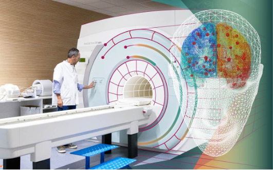
HBP researchers have employed highly advanced methods from computing, neuroinformatics and artificial intelligence in a truly integrative approach to understanding the brain as a multi-level system. The project has contributed to a deeper understanding of the complex structure and function of the brain and enabled novel applications in medicine and technological advances.

Among the project’s highlight achievements are a three-dimensional, digital atlas of the human brain with unprecedented detail, personalised virtual models of patient brains with conditions like epilepsy and Parkinson’s, breakthroughs in the field of artificial intelligence, and an open digital research infrastructure – EBRAINS – that will remain an invaluable resource for the entire neuroscience community beyond the end of the HBP.

Researchers at the HBP have presented scientific results in over 3000 publications, as well as advanced medical and technical applications and over 160 freely accessible digital tools for neuroscience research.

“The Human Brain Project has a pioneering role for digital brain research with a unique interdisciplinary approach at the interface of neuroscience, computing and technology,” says Katrin Amunts, Director of the HBP and of the Institute for Neuroscience and Medicine at FZJ. “EBRAINS will continue to power this new way of investigating the brain and foster developments in brain medicine.”

“The impact of what you achieved in digital science goes beyond the neuroscientific community”, said Gustav Kalbe, CNECT, Acting Director of Digital Excellence and Science Infrastructures at the European Commission during the opening of the event. “The infrastructure that the Human Brain Project has established is already seen as a key building block to facilitate cooperation and research across geographical boundaries, but also across communities.”

Further information about the Human Brain Project as well as photos from research can be found here: https://fz-juelich.sciebo.de/s/hWJkNCC1Hi1PdQ5.

Results highlights and event photos in the online press release.

Results overviews:
– “Human Brain Project: Spotlights on major achievements” and “A closer Look on Scientific
Advances”

– “Human Brain Project: An extensive guide to the tools developed”

Examples of results from the Human Brain Project:

As the “Google Maps of the brain” [emphasis mine], the Human Brain Project makes the most comprehensive digital brain atlas to date available to all researchers worldwide. The atlas by Jülich researchers and collaborators combines high-resolution data of neurons, fibre connections, receptors and functional specialisations in the brain, and is designed as a constantly growing system.

13 hospitals in France are currently testing the new “Virtual Epileptic Patient” – a platform developed at the University of Marseille [Aix-Marseille University?] in the Human Brain Project. It creates personalised simulation models of brain dynamics to provide surgeons with predictions for the success of different surgical treatment strategies. The approach was presented this year in the journals Science Translational Medicine and The Lancet Neurology.


SpiNNaker2 is a “neuromorphic” [brainlike] computer developed by the University of Manchester and TU Dresden within the Human Brain Project. The company SpiNNcloud Systems in Dresden is commercialising the approach for AI applications. (Image: Sprind.org)

As an openly accessible digital infrastructure, EBRAINS offers scientists easy access to the best techniques for complex research questions.

[https://www.ebrains.eu/]

There was a Canadian connection at one time; Montréal Neuro at Canada’s McGill University was involved in developing a computational platform for neuroscience (CBRAIN) for HBP according to an announcement in my January 29, 2013 posting. However, there’s no mention of the EU project on the CBRAIN website nor is there mention of a Canadian partner on the EBRAINS website, which seemed the most likely successor to the CBRAIN portion of the HBP project originally mentioned in 2013.

I couldn’t resist “Google maps of the brain.”

In any event, the statement from Astrid Lambrecht offers an interesting contrast to that offered by the leader of the other project.

Graphene Flagship

In fact, the Graphene Flagship has been celebrating its 10th anniversary since last year; see my September 1, 2022 posting titled “Graphene Week (September 5 – 9, 2022) is a celebration of 10 years of the Graphene Flagship.”

The flagship’s lead institution, Chalmers University of Technology in Sweden, issued an August 28, 2023 press release by Lisa Gahnertz (also on the Graphene Flagship website but published September 4, 2023) touting its achievement with an ebullience I am more accustomed to seeing in US news releases,

Chalmers steers Europe’s major graphene venture to success

For the past decade, the Graphene Flagship, the EU’s largest ever research programme, has been coordinated from Chalmers with Jari Kinaret at the helm. As the project reaches the ten-year mark, expectations have been realised, a strong European research field on graphene has been established, and the journey will continue.

‘Have we delivered what we promised?’ asks Graphene Flagship Director Jari Kinaret from his office in the physics department at Chalmers, overlooking the skyline of central Gothenburg.

‘Yes, we have delivered more than anyone had a right to expect,’ [emphasis mine] he says. ‘In our analysis for the conclusion of the project, we read the documents that were written at the start. What we promised then were over a hundred specific things. Some of them were scientific and technological promises, and they have all been fulfilled. Others were for specific applications, and here 60–70 per cent of what was promised has been delivered. We have also delivered applications we did not promise from the start, but these are more difficult to quantify.’

The autumn of 2013 saw the launch of the massive ten-year Science, Technology and Innovation research programme on graphene and other related two-dimensional materials. Joint funding from the European Commission and EU Member States totalled a staggering €1,000 million. A decade later, it is clear that the large-scale initiative has succeeded in its endeavours. According to a report by the research institute WifOR, the Graphene Flagship will have created a total contribution to GDP of €3,800 million and 38,400 new jobs in the 27 EU countries between 2014 and 2030.

Exceeded expectations

‘Per euro invested and compared to other EU projects, the flagship has performed 13 times better than expected in terms of patent applications, and seven times better for scientific publications. We have 17 spin-off companies that have received over €130 million in private funding – people investing their own money is a real example of trust in the fact that the technology works,’ says Jari Kinaret.

He emphasises that the long time span has been crucial in developing the concepts of the various flagship projects.

‘When it comes to new projects, the ability to work on a long timescale is a must and is more important than a large budget. It takes a long time to build trust, both in one another within a team and in the technology on the part of investors, industry and the wider community. The size of the project has also been significant. There has been an ecosystem around the material, with many graphene manufacturers and other organisations involved. It builds robustness, which means you have the courage to invest in the material and develop it.’

From lab to application

In 2010, Andre Geim and Konstantin Novoselov of the University of Manchester won the Nobel Prize in Physics for their pioneering experiments isolating the ultra-light and ultra-thin material graphene. It was the first known 2D material and stunned the world with its ‘exceptional properties originating in the strange world of quantum physics’ according to the Nobel Foundation’s press release. Many potential applications were identified for this electrically conductive, heat-resistant and light-transmitting material. Jari Kinaret’s research team had been exploring the material since 2006, and when Kinaret learned of the European Commission’s call for a ten-year research programme, it prompted him to submit an application. The Graphene Flagship was initiated to ensure that Europe would maintain its leading position in graphene research and innovation, and its coordination and administration fell to Chalmers.

Is it a staggering thought that your initiative became the biggest EU research project of all time?

‘The fact that the three-minute presentation I gave at a meeting in Brussels has grown into an activity in 22 countries, with 170 organisations and 1,300 people involved … You can’t think about things like that because it can easily become overwhelming. Sometimes you just have to go for it,’ says Jari Kinaret.

One of the objectives of the Graphene Flagship was to take the hopes for this material and move them from lab to application. What has happened so far?

‘We are well on track with 100 products priced and on their way to the market. Many of them are business-to-business products that are not something we ordinary consumers are going to buy, but which may affect us indirectly.’

‘It’s important to remember that getting products to the application stage is a complex process. For a researcher, it may take ten working prototypes; for industry, ten million. Everything has to click into place, on a large scale. All components must work identically and in exactly the same way, and be compatible with existing production in manufacturing as you cannot rebuild an entire factory for a new material. In short, it requires reliability, reproducibility and manufacturability.’

Applications in a wide range of areas

Graphene’s extraordinary properties are being used to deliver the next generation of technologies in a wide range of fields, such as sensors for self-driving cars, advanced batteries, new water purification methods and sophisticated instruments for use in neuroscience. When asked if there are any applications that Jani Kinaret himself would like to highlight, he mentions, among other things, the applications that are underway in the automotive industry – such as sensors to detect obstacles for self-driving cars. Thanks to graphene, they will be so cost-effective to produce that it will be possible to make them available in more than just the most expensive car models.

He also highlights the aerospace industry, where a graphene material for removing ice from aircraft and helicopter wings is under development for the Airbus company. Another favourite, which he has followed from basic research to application, is the development of an air cleaner for Lufthansa passenger aircraft, based on a kind of ‘graphene foam’. Because graphene foam is very light, it can be heated extremely quickly. A pulse of electricity lasting one thousandth of a second is enough to raise the temperature to 300 degrees, thus killing micro-organisms and effectively cleaning the air in the aircraft.

He also mentions the Swedish company ABB, which has developed a graphene composite for circuit breakers in switchgear. These circuit breakers are used to protect the electricity network and must be safe to use. The graphene composite replaces the manual lubrication of the circuit breakers, resulting in significant cost savings.

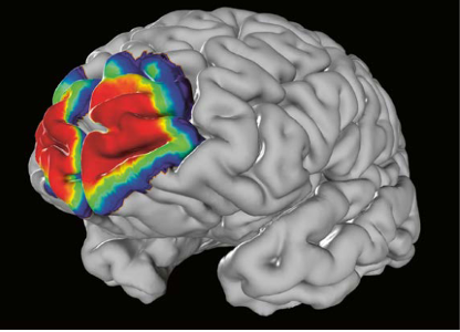
‘We also see graphene being used in medical technology, but its application requires many years of testing and approval by various bodies. For example, graphene technology can more effectively map the brain before neurosurgery, as it provides a more detailed image. Another aspect of graphene is that it is soft and pliable. This means it can be used for electrodes that are implanted in the brain to treat tremors in Parkinson’s patients, without the electrodes causing scarring,’ says Jari Kinaret.

Coordinated by Chalmers

Jari Kinaret sees the fact that the EU chose Chalmers as the coordinating university as a favourable factor for the Graphene Flagship.

‘Hundreds of millions of SEK [Swedish Kroner] have gone into Chalmers research, but what has perhaps been more important is that we have become well-known and visible in certain areas. We also have the 2D-Tech competence centre and the SIO Grafen programme, both funded by Vinnova and coordinated by Chalmers and Chalmers industriteknik respectively. I think it is excellent that Chalmers was selected, as there could have been too much focus on the coordinating organisation if it had been more firmly established in graphene research at the outset.’

What challenges have been encountered during the project?

‘With so many stakeholders involved, we are not always in agreement. But that is a good thing. A management book I once read said that if two parties always agree, then one is redundant. At the start of the project, it was also interesting to see the major cultural differences we had in our communications and that different cultures read different things between the lines; it took time to realise that we should be brutally straightforward in our communications with one another.’

What has it been like to have the coordinating role that you have had?

‘Obviously, I’ve had to worry about things an ordinary physics professor doesn’t have to worry about, like a phone call at four in the morning after the Brexit vote or helping various parties with intellectual property rights. I have read more legal contracts than I thought I would ever have to read as a professor. As a researcher, your approach when you go into a role is narrow and deep, here it was rather all about breadth. I would have liked to have both, but there are only 26 hours in a day,’ jokes Jari Kinaret.

New phase for the project and EU jobs to come

A new assignment now awaits Jari Kinaret outside Chalmers as Chief Executive Officer of the EU initiative KDT JU (Key Digital Technologies Joint Undertaking, soon to become Chips JU), where industry and the public sector interact to drive the development of new electronic components and systems.

The Graphene Flagship may have reached its destination in its current form, but the work started is progressing in a form more akin to a flotilla. About a dozen projects will continue to live on under the auspices of the European Commission’s Horizon Europe programme. Chalmers is going to coordinate a smaller CSA project called GrapheneEU, where CSA stands for ‘Coordination and Support Action’. It will act as a cohesive force between the research and innovation projects that make up the next phase of the flagship, offering them a range of support and services, including communication, innovation and standardisation.

The Graphene Flagship is about to turn ten. If the project had been a ten-year-old child, what kind of child would it have been?

‘It would have been a very diverse organism. Different aspirations are beginning to emerge – perhaps it is adolescence that is approaching. In addition, within the project we have also studied other related 2D materials, and we found that there are 6,000 distinct materials of this type, of which only about 100 have been studied. So, it’s the younger siblings that are starting to arrive now.’

Facts about the Graphene Flagship:

The Graphene Flagship is the first European flagship for future and emerging technologies. It has been coordinated and administered from the Department of Physics at Chalmers, and as the project enters its next phase, GrapheneEU, coordination will continue to be carried out by staff currently working on the flagship led by Chalmers Professor Patrik Johansson.

The project has proved highly successful in developing graphene-based technology in Europe, resulting in 17 new companies, around 100 new products, nearly 500 patent applications and thousands of scientific papers. All in all, the project has exceeded the EU’s targets for utilisation from research projects by a factor of ten. According to the assessment of the EU research programme Horizon 2020, Chalmers’ coordination of the flagship has been identified as one of the key factors behind its success.

Graphene Week will be held at the Svenska Mässan in Gothenburg from 4 to 8 September 2023. Graphene Week is an international conference, which also marks the finale of the ten-year anniversary of the Graphene Flagship. The conference will be jointly led by academia and industry – Professor Patrik Johansson from Chalmers and Dr Anna Andersson from ABB – and is expected to attract over 400 researchers from Sweden, Europe and the rest of the world. The programme includes an exhibition, press conference and media activities, special sessions on innovation, diversity and ethics, and several technical sessions. The full programme is available here.

Read the press release on Graphene Week from 4 to 8 September and the overall results of the Graphene Flagship. …

Ten years and €1B each. Congratulations to the organizers on such massive undertakings. As for whether or not (and how they’ve been successful), I imagine time will tell.

Optical memristors and neuromorphic computing

A June 5, 2023 news item on Nanowerk announced a paper which reviews the state-of-the-art of optical memristors, Note: Links have been removed,

AI, machine learning, and ChatGPT may be relatively new buzzwords in the public domain, but developing a computer that functions like the human brain and nervous system – both hardware and software combined – has been a decades-long challenge. Engineers at the University of Pittsburgh are today exploring how optical “memristors” may be a key to developing neuromorphic computing.

Resistors with memory, or memristors, have already demonstrated their versatility in electronics, with applications as computational circuit elements in neuromorphic computing and compact memory elements in high-density data storage. Their unique design has paved the way for in-memory computing and captured significant interest from scientists and engineers alike.

A new review article published in Nature Photonics (“Integrated Optical Memristors”), sheds light on the evolution of this technology—and the work that still needs to be done for it to reach its full potential. Led by Nathan Youngblood, assistant professor of electrical and computer engineering at the University of Pittsburgh Swanson School of Engineering, the article explores the potential of optical devices which are analogs of electronic memristors. This new class of device could play a major role in revolutionizing high-bandwidth neuromorphic computing, machine learning hardware, and artificial intelligence in the optical domain.

A June 2, 2023 University of Pittsburgh news release (also on EurekAlert but published June 5, 2023), which originated the news item, provides more detail,

“Researchers are truly captivated by optical memristors because of their incredible potential in high-bandwidth neuromorphic computing, machine learning hardware, and artificial intelligence,” explained Youngblood. “Imagine merging the incredible advantages of optics with local information processing. It’s like opening the door to a whole new realm of technological possibilities that were previously unimaginable.” 

The review article presents a comprehensive overview of recent progress in this emerging field of photonic integrated circuits. It explores the current state-of-the-art and highlights the potential applications of optical memristors, which combine the benefits of ultrafast, high-bandwidth optical communication with local information processing. However, scalability emerged as the most pressing issue that future research should address. 

“Scaling up in-memory or neuromorphic computing in the optical domain is a huge challenge. Having a technology that is fast, compact, and efficient makes scaling more achievable and would represent a huge step forward,” explained Youngblood. 

“One example of the limitations is that if you were to take phase change materials, which currently have the highest storage density for optical memory, and try to implement a relatively simplistic neural network on-chip, it would take a wafer the size of a laptop to fit all the memory cells needed,” he continued. “Size matters for photonics, and we need to find a way to improve the storage density, energy efficiency, and programming speed to do useful computing at useful scales.”

Using Light to Revolutionize Computing

Optical memristors can revolutionize computing and information processing across several applications. They can enable active trimming of photonic integrated circuits (PICs), allowing for on-chip optical systems to be adjusted and reprogrammed as needed without continuously consuming power. They also offer high-speed data storage and retrieval, promising to accelerate processing, reduce energy consumption, and enable parallel processing. 

Optical memristors can even be used for artificial synapses and brain-inspired architectures. Dynamic memristors with nonvolatile storage and nonlinear output replicate the long-term plasticity of synapses in the brain and pave the way for spiking integrate-and-fire computing architectures.

Research to scale up and improve optical memristor technology could unlock unprecedented possibilities for high-bandwidth neuromorphic computing, machine learning hardware, and artificial intelligence. 

“We looked at a lot of different technologies. The thing we noticed is that we’re still far away from the target of an ideal optical memristor–something that is compact, efficient, fast, and changes the optical properties in a significant manner,” Youngblood said. “We’re still searching for a material or a device that actually meets all these criteria in a single technology in order for it to drive the field forward.”

The publication of “Integrated Optical Memristors” (DOI: 10.1038/s41566-023-01217-w) was published in Nature Photonics and is coauthored by senior author Harish Bhaskaran at the University of Oxford, Wolfram Pernice at Heidelberg University, and Carlos Ríos at the University of Maryland.

Despite including that final paragraph, I’m also providing a link to and a citation for the paper,

Integrated optical memristors by Nathan Youngblood, Carlos A. Ríos Ocampo, Wolfram H. P. Pernice & Harish Bhaskaran. Nature Photonics volume 17, pages 561–572 (2023) DOI: https://doi.org/10.1038/s41566-023-01217-w Published online: 29 May 2023 Issue Date: July 2023

This paper is behind a paywall.

Memristors based on halide perovskite nanocrystals are more powerful and easier to manufacture

A March 8, 2023 news item on phys.org announces research from Swiss and Italian researchers into a new type of memristor,

Researchers at Empa, ETH Zurich and the Politecnico di Milano are developing a new type of computer component that is more powerful and easier to manufacture than its predecessors. Inspired by the human brain, it is designed to process large amounts of data fast and in an energy-efficient way.

In many respects, the human brain is still superior to modern computers. Although most people can’t do math as fast as a computer, we can effortlessly process complex sensory information and learn from experiences, while a computer cannot – at least not yet. And, the brain does all this by consuming less than half as much energy as a laptop.

One of the reasons for the brain’s energy efficiency is its structure. The individual brain cells – the neurons and their connections, the synapses – can both store and process information. In computers, however, the memory is separate from the processor, and data must be transported back and forth between these two components. The speed of this transfer is limited, which can slow down the whole computer when working with large amounts of data.

One possible solution to this bottleneck are novel computer architectures that are modeled on the human brain. To this end, scientists are developing so-called memristors: components that, like brain cells, combine data storage and processing. A team of researchers from Empa, ETH Zurich and the “Politecnico di Milano” has now developed a memristor that is more powerful and easier to manufacture than its predecessors. The researchers have recently published their results in the journal Science Advances.

A March 8, 2023 Swiss Federal Laboratories for Materials Science and Technology (EMPA) press release (also on EurekAlert), which originated the news item, provides details about what makes this memristor different,

Performance through mixed ionic and electronic conductivity

The novel memristors are based on halide perovskite nanocrystals, a semiconductor material known from solar cell manufacturing. “Halide perovskites conduct both ions and electrons,” explains Rohit John, former ETH Fellow and postdoctoral researcher at both ETH Zurich and Empa. “This dual conductivity enables more complex calculations that closely resemble processes in the brain.”

The researchers conducted the experimental part of the study entirely at Empa: They manufactured the thin-film memristors at the Thin Films and Photovoltaics laboratory and investigated their physical properties at the Transport at Nanoscale Interfaces laboratory. Based on the measurement results, they then simulated a complex computational task that corresponds to a learning process in the visual cortex in the brain. The task involved determining the orientation of light based on signals from the retina.

“As far as we know, this is only the second time this kind of computation has been performed on memristors,” says Maksym Kovalenko, professor at ETH Zurich and head of the Functional Inorganic Materials research group at Empa. “At the same time, our memristors are much easier to manufacture than before.” This is because, in contrast to many other semiconductors, perovskites crystallize at low temperatures. In addition, the new memristors do not require the complex preconditioning through application of specific voltages that comparable devices need for such computing tasks. This makes them faster and more energy-efficient.

Complementing rather than replacing

The technology, though, is not quite ready for deployment yet. The ease with which the new memristors can be manufactured also makes them difficult to integrate with existing computer chips: Perovskites cannot withstand temperatures of 400 to 500 degrees Celsius that are needed to process silicon – at least not yet. But according to Daniele Ielmini, professor at the “Politecnico di Milano”, that integration is key to the success for new brain-like computer technologies. “Our goal is not to replace classical computer architecture,” he explains. “Rather, we want to develop alternative architectures that can perform certain tasks faster and with greater energy efficiency. This includes, for example, the parallel processing of large amounts of data, which is generated everywhere today, from agriculture to space exploration.”

Promisingly, there are other materials with similar properties that could be used to make high-performance memristors. “We can now test our memristor design with different materials,” says Alessandro Milozzi, a doctoral student at the “Politecnico di Milano”. “It is quite possible that some of them are better suited for integration with silicon.”

Here’s a link to and a citation for the paper,

Ionic-electronic halide perovskite memdiodes enabling neuromorphic computing with a second-order complexity by Rohit Abraham John, Alessandro Milozzi, Sergey Tsarev, Rolf Brönnimann, Simon C. Boehme, Erfu Wu, Ivan Shorubalko, Maksym V. Kovalenko, and Daniele Ielmini. Science Advances 23 Dec 2022 Vol 8, Issue 51 DOI: 10.1126/sciadv.ade0072

This paper is open access.