Tag Archives: Michael Berger

Butterfly mating inspires neuromorphic (brainlike) computing

Michael Berger writes about a multisensory approach to neuromorphic computing inspired by butterflies in his February 2, 2024 Nanowerk Spotlight article, Note: Links have been removed,

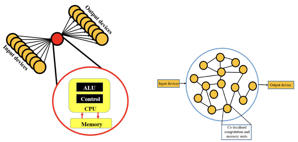
Artificial intelligence systems have historically struggled to integrate and interpret information from multiple senses the way animals intuitively do. Humans and other species rely on combining sight, sound, touch, taste and smell to better understand their surroundings and make decisions. However, the field of neuromorphic computing has largely focused on processing data from individual senses separately.

This unisensory approach stems in part from the lack of miniaturized hardware able to co-locate different sensing modules and enable in-sensor and near-sensor processing. Recent efforts have targeted fusing visual and tactile data. However, visuochemical integration, which merges visual and chemical information to emulate complex sensory processing such as that seen in nature—for instance, butterflies integrating visual signals with chemical cues for mating decisions—remains relatively unexplored. Smell can potentially alter visual perception, yet current AI leans heavily on visual inputs alone, missing a key aspect of biological cognition.

Now, researchers at Penn State University have developed bio-inspired hardware that embraces heterogeneous integration of nanomaterials to allow the co-location of chemical and visual sensors along with computing elements. This facilitates efficient visuochemical information processing and decision-making, taking cues from the courtship behaviors of a species of tropical butterfly.

In the paper published in Advanced Materials (“A Butterfly-Inspired Multisensory Neuromorphic Platform for Integration of Visual and Chemical Cues”), the researchers describe creating their visuochemical integration platform inspired by Heliconius butterflies. During mating, female butterflies rely on integrating visual signals like wing color from males along with chemical pheromones to select partners. Specialized neurons combine these visual and chemical cues to enable informed mate choice.

To emulate this capability, the team constructed hardware encompassing monolayer molybdenum disulfide (MoS2) memtransistors serving as visual capture and processing components. Meanwhile, graphene chemitransistors functioned as artificial olfactory receptors. Together, these nanomaterials provided the sensing, memory and computing elements necessary for visuochemical integration in a compact architecture.

While mating butterflies served as inspiration, the developed technology has much wider relevance. It represents a significant step toward overcoming the reliance of artificial intelligence on single data modalities. Enabling integration of multiple senses can greatly improve situational understanding and decision-making for autonomous robots, vehicles, monitoring devices and other systems interacting with complex environments.

The work also helps progress neuromorphic computing approaches seeking to emulate biological brains for next-generation ML acceleration, edge deployment and reduced power consumption. In nature, cross-modal learning underpins animals’ adaptable behavior and intelligence emerging from brains organizing sensory inputs into unified percepts. This research provides a blueprint for hardware co-locating sensors and processors to more closely replicate such capabilities

It’s fascinating to me how many times butterflies inspire science,

Butterfly-inspired visuo-chemical integration. a) A simplified abstraction of visual and chemical stimuli from male butterflies and visuo-chemical integration pathway in female butterflies. b) Butterfly-inspired neuromorphic hardware comprising of monolayer MoS2 memtransistor-based visual afferent neuron, graphene-based chemoreceptor neuron, and MoS2 memtransistor-based neuro-mimetic mating circuits. Courtesy: Wiley/Penn State University Researchers

Here’s a link to and a citation for the paper,

A Butterfly-Inspired Multisensory Neuromorphic Platform for Integration of Visual and Chemical Cues by Yikai Zheng, Subir Ghosh, Saptarshi Das. Advanced Materials SOI: https://doi.org/10.1002/adma.202307380 First published: 09 December 2023

This paper is open access.

Neuromorphic engineering: an overview

In a February 13, 2023 essay, Michael Berger who runs the Nanowerk website provides an overview of brainlike (neuromorphic) engineering.

This essay is the most extensive piece I’ve seen on Berger’s website and it covers everything from the reasons why scientists are so interested in mimicking the human brain to specifics about memristors. Here are a few excerpts (Note: Links have been removed),

Neuromorphic engineering is a cutting-edge field that focuses on developing computer hardware and software systems inspired by the structure, function, and behavior of the human brain. The ultimate goal is to create computing systems that are significantly more energy-efficient, scalable, and adaptive than conventional computer systems, capable of solving complex problems in a manner reminiscent of the brain’s approach.

This interdisciplinary field draws upon expertise from various domains, including neuroscience, computer science, electronics, nanotechnology, and materials science. Neuromorphic engineers strive to develop computer chips and systems incorporating artificial neurons and synapses, designed to process information in a parallel and distributed manner, akin to the brain’s functionality.

Key challenges in neuromorphic engineering encompass developing algorithms and hardware capable of performing intricate computations with minimal energy consumption, creating systems that can learn and adapt over time, and devising methods to control the behavior of artificial neurons and synapses in real-time.

Neuromorphic engineering has numerous applications in diverse areas such as robotics, computer vision, speech recognition, and artificial intelligence. The aspiration is that brain-like computing systems will give rise to machines better equipped to tackle complex and uncertain tasks, which currently remain beyond the reach of conventional computers.

It is essential to distinguish between neuromorphic engineering and neuromorphic computing, two related but distinct concepts. Neuromorphic computing represents a specific application of neuromorphic engineering, involving the utilization of hardware and software systems designed to process information in a manner akin to human brain function.

One of the major obstacles in creating brain-inspired computing systems is the vast complexity of the human brain. Unlike traditional computers, the brain operates as a nonlinear dynamic system that can handle massive amounts of data through various input channels, filter information, store key information in short- and long-term memory, learn by analyzing incoming and stored data, make decisions in a constantly changing environment, and do all of this while consuming very little power.

The Human Brain Project [emphasis mine], a large-scale research project launched in 2013, aims to create a comprehensive, detailed, and biologically realistic simulation of the human brain, known as the Virtual Brain. One of the goals of the project is to develop new brain-inspired computing technologies, such as neuromorphic computing.

The Human Brain Project has been funded by the European Union (1B Euros over 10 years starting in 2013 and sunsetting in 2023). From the Human Brain Project Media Invite,

The final Human Brain Project Summit 2023 will take place in Marseille, France, from March 28-31, 2023.

As the ten-year European Flagship Human Brain Project (HBP) approaches its conclusion in September 2023, the final HBP Summit will highlight the scientific achievements of the project at the interface of neuroscience and technology and the legacy that it will leave for the brain research community. …

One last excerpt from the essay,

Neuromorphic computing is a radical reimagining of computer architecture at the transistor level, modeled after the structure and function of biological neural networks in the brain. This computing paradigm aims to build electronic systems that attempt to emulate the distributed and parallel computation of the brain by combining processing and memory in the same physical location.

This is unlike traditional computing, which is based on von Neumann systems consisting of three different units: processing unit, I/O unit, and storage unit. This stored program architecture is a model for designing computers that uses a single memory to store both data and instructions, and a central processing unit to execute those instructions. This design, first proposed by mathematician and computer scientist John von Neumann, is widely used in modern computers and is considered to be the standard architecture for computer systems and relies on a clear distinction between memory and processing.

I found the diagram Berger Included with von Neumann’s design contrasted with a neuromorphic design illuminating,

A graphical comparison of the von Neumann and Neuromorphic architecture. Left: The von Neumann architecture used in traditional computers. The red lines depict the data communication bottleneck in the von Neumann architecture. Right: A graphical representation of a general neuromorphic architecture. In this architecture, the processing and memory is decentralized across different neuronal units(the yellow nodes) and synapses(the black lines connecting the nodes), creating a naturally parallel computing environment via the mesh-like structure. (Source: DOI: 10.1109/IS.2016.7737434) [downloaded from https://www.nanowerk.com/spotlight/spotid=62353.php]

Berger offers a very good overview and I recommend reading his February 13, 2023 essay on neuromorphic engineering with one proviso, Note: A link has been removed,

Many researchers in this field see memristors as a key device component for neuromorphic engineering. Memristor – or memory resistor – devices are non-volatile nanoelectronic memory devices that were first theorized [emphasis mine] by Leon Chua in the 1970’s. However, it was some thirty years later that the first practical device was fabricated in 2008 by a group led by Stanley Williams [sometimes cited as R. Stanley Williams] at HP Research Labs.

Chua wasn’t the first as he, himself, has noted. Chua arrived at his theory independently in the 1970s but Bernard Widrow theorized what he called a ‘memistor’ in the 1960s. In fact “Memristors: they are older than you think” is a May 22, 2012 posting which featured an article “Two centuries of memristors” by Themistoklis Prodromakis, Christofer Toumazou and Leon Chua published in Nature Materials.

Most of us try to get it right but we don’t always succeed. It’s always good practice to read everyone (including me) with a little skepticism.

Living optical fibers

The word ‘living’ isn’t usually associated with optical fibers and the addition had me thinking that this October 11, 2021 Nanowerk Spotlight story by Michael Berger would be a synthetic biology story. Well, not exactly. Do read on for a good introduction describing glass, fiber optics, and optogenetics,

Glass is one of the oldest manufactured materials used by humans and glass making dates back at least 6000 years, long before humans had discovered how to smelt iron. Glasses have been based on the chemical compound silica – silicon dioxide, or quartz – the primary constituent of sand. Soda-lime glass, containing around 70% silica, accounts for around 90% of manufactured glass.

Historically, we are familiar with glasses’ decorative use or as window panes, household items, and in optics such as eyeglasses, microscopes and telescopes. More recently, starting in the 1950s, glass has been used in the manufacture of fiber optic cables, a technology that has revolutionized the communications industry and helped ring in the digital revolution.

Fiber optic cables propagate a signal as a pulse of light along a transparent medium, usually glass. This is not only used to transmit information but, for instance in many healthcare and biomedical applications, scientists use optical fibers for sensing applications by shining light into a sample and evaluating the absorbed or transmitted light.

A recent development in this field is optogenetics, a neuromodulation method that uses activation or deactivation of brain cells by illumination with different colors of light in order to treat brain disorders.

Berger goes on to explain the latest work and reveals what ‘living’ means where this work is concerned,

This work represents a simple and low-cost approach to fabricating optical fibers made from biological materials. These fibers can be easily modified for specific applications and don’t require sophisticated equipment to generate relevant information. This method could be used for many practical sensing and biological modeling applications.

“We use a natural, ionic, and biologically compatible crosslinking approach, which enables us to produce flexible hydrogel fibers in continuous multi-layered architectures, meaning they are easy to produce and can be modified after fabrication,” explains Guimarães [Carlos Guimarães, the paper’s first author]. “Similarly to silica fibers, the core hydrogel of our structures can be exposed, fused to another fiber or reassembled if they break, and efficiently guide light through the established connection.”

These flexible hydrogel fibers are made from sugars and work just like solid-state optical fibers used to transmit data. However, they are biocompatible so they can be easily integrated with biological systems.

“We could even consider them to be alive [emphasis mine] since we can use them to grow living cells inside the fiber,” says Guimarães. “As these embedded cells grow over time, we can then use light to inform on living dynamic events, for example to track cancer invasive proliferation into optical information.” [emphasis mine]

As to what constitutes optical information in this context,

Another intriguing aspect of these hydrogel fibers is that their permeable mesh enables the inclusion of biological targets of interest for detection. For example, the scientists observed that fibers were able to soak SARS-CoV-2 viruses, and by integrating nanoparticles for their binding and detection, shifts in visible light could be observed for detecting the accumulation of viral particles within the fiber.

“When light moving through the fiber encounters living cells, it changes its characteristics depending on cellular density, invasive proliferation, expression of molecules, etc.” Guimarães notes. “This light-cell interaction can digitize complex biological events, converting responses such as cancer cell progression in 3D environments and susceptibility to drugs into numbers and data, very fast and without the need for sample destruction.”

Here’s a link to and a citation for the paper,

Engineering Polysaccharide-Based Hydrogel Photonic Constructs: From Multiscale Detection to the Biofabrication of Living Optical Fibers by Carlos F. Guimarães, Rajib Ahmed, Amideddin Mataji-Kojouri, Fernando Soto, Jie Wang, Shiqin Liu, Tanya Stoyanova, Alexandra P. Marques, Rui L. Reis, Utkan Demirci. Advanced Materials DOI: https://doi.org/10.1002/adma.202105361 First published: 07 October 2021

This paper is behind a paywall.

Artificial intelligence (AI) designs “Giants of Nanotech” non-fungible tokens (NFTs)

Nanowerk, an agency which provides nanotechnology information and more, has commissioned a series of AI-designed non-fungible tokens representing two of the ‘Giants of Nanotechnology’, Richard Feynman and Sir Harold Kroto.

It’s a fundraising effort as noted here in an April 10, 2022 Nanowerk Spotlight article by website owner, Michael Berger,

We’ve spent a lot of time recently researching and writing the articles for our Smartworlder section here on Nanowerk – about cryptocurrencies, explaining blockchain, and many other aspects of smart technologies – for instance non-fungible tokens (NFTs). So, we thought: Why not go all the way and try this out ourselves?

As many organizations continue to push the boundaries as to what is possible within the web3 ecosystem, producing our first-ever collection of nanotechnology-themed digital art on the blockchain seemed like a natural extension for our brand and we hope that these NFT collectibles will be cherished by our reader community.

To start with, we created two inaugural Nanowerk NFT collections in a series we are calling Giants of Nanotech in order to honor the great minds of science in this field.

The digital artwork has been created using the artificial intelligence (AI) image creation algorithm Neural Style Transfer. This technique takes two images – a content image and a style reference image (such as an artwork by a famous painter) – and blends them together so the output image looks like the content image, but ‘painted’ in the style of the reference image.

For example, here is a video clip that shows how the AI transforms the Feynman content image into a painting inspired by Victor Nunnally’s Journey Man:

If you want to jump right into it, here are the Harry Kroto collection and the Richard Feynman collection on the OpenSea marketplace.

Have fun with our NFTs and please remember, your purchase helps fund Nanowerk and we are very grateful to you!

Also note: NFTs are an extremely volatile market. This article is not financial advice. Invest in the crypto and NFT market at your own risk. Only invest if you fully understand the potential risks.

I have a couple of comments. First, there’s Feynman’s status as a ‘Giant of Nanotechnology’. He is credited in the US as providing a foundational text (a 1959 lecture titled “There’s Plenty of Room at the Bottom”) for the field of nanotechnology. There has been some controversy over the lecture’s influence some of which has been covered in the Wikipedia entry titled, “There’s Plenty of Room at the Bottom.”

Second, Sir Harold Kroto won the 1996 Nobel Prize for Chemistry, along with two colleagues (all three were at Rice University in Texas), for the discovery of the buckminsterfullerene. Here’s more about that from the Richard E. Smalley, Robert F. Curl, and Harold W. Kroto essay on the Science History Institute website,

In 1996 three scientists, two American and one British, shared the Nobel Prize in Chemistry for their discovery of buckminsterfullerene (the “buckyball”) and other fullerenes. These “carbon cages” resembling soccer balls opened up a whole new field of chemical study with practical applications in materials science, electronics, and nanotechnology that researchers are only beginning to uncover.

With their discovery of buckminsterfullerene in 1985, Richard E. Smalley (1943–2005), Robert F. Curl (b. 1933), and Harold W. Kroto (1939–2016) furthered progress to the long-held objective of molecular-scale electronics and other nanotechnologies. …

Finally, good luck to Nanowerk and Michael Berger.

Plug me in: how to power up ingestible and implantable electroncis

From time to time I’ve featured ‘vampire technology’, a name I vastly prefer to energy harvesting or any of its variants. The focus has usually been on implantable electronic devices such as pacemakers and deep brain stimulators.

In this February 16, 2021 Nanowerk Spotlight article, Michael Berger broadens the focus to include other electronic devices,

Imagine edible medical devices that can be safely ingested by patients, perform a test or release a drug, and then transmit feedback to your smartphone; or an ingestible, Jell-O-like pill that monitors the stomach for up to a month.

Devices like these, as well as a wide range of implantable biomedical electronic devices such as pacemakers, neurostimulators, subdermal blood sensors, capsule endoscopes, and drug pumps, can be useful tools for detecting physiological and pathophysiological signals, and providing treatments performed inside the body.

Advances in wireless communication enable medical devices to be untethered when in the human body. Advances in minimally invasive or semi-invasive surgical implantation procedures have enabled biomedical devices to be implanted in locations where clinically important biomarkers and physiological signals can be detected; it has also enabled direct administration of medication or treatment to a target location.

However, one major challenge in the development of these devices is the limited lifetime of their power sources. The energy requirements of biomedical electronic devices are highly dependent on their application and the complexity of the required electrical systems.

Berger’s commentary was occasioned by a review article in Advanced Functional Materials (link and citation to follow at the end of this post). Based on this review, the February 16, 2021 Nanowerk Spotlight article provides insight into the current state of affairs and challenges,

Biomedical electronic devices can be divided into three main categories depending on their application: diagnostic, therapeutic, and closed-loop systems. Each category has a different degree of complexity in the electronic system.

… most biomedical electronic devices are composed of a common set of components, including a power unit, sensors, actuators, a signal processing and control unit, and a data storage unit. Implantable and ingestible devices that require a great deal of data manipulation or large quantities of data logging also need to be wirelessly connected to an external device so that data can be transmitted to an external receiver and signal processing, data storage, and display can be performed more efficiently.

The power unit, which is composed of one or more energy sources – batteries, energy-harvesting, and energy transfer – as well as power management circuits, supplies electrical energy to the whole system.

Implantable medical devices such as cardiac pacemakers, neurostimulators and drug delivery devices are major medical tools to support life activity and provide new therapeutic strategies. Most such devices are powered by lithium batteries whose service life is as low as 10 years. Hence, many patients must undergo a major surgery to check the battery performance and replace the batteries as necessary.

In the last few decades, new battery technology has led to increases in the performance, reliability, and lifetime of batteries. However, challenges remain, especially in terms of volumetric energy density and safety.

Electronic miniaturization allows more functionalities to be added to devices, which increases power requirements. Recently, new material-based battery systems have been developed with higher energy densities.

Different locations and organ systems in the human body have access to different types of energy sources, such as mechanical, chemical, and electromagnetic energies.

Energy transfer technologies can deliver energy from outside the body to implanted or ingested devices. If devices are implanted at the locations where there are no accessible endogenous energies, exogenous energies in the form of ultrasonic or electromagnetic waves can penetrate through the biological barriers and wirelessly deliver the energies to the devices.

Both images embedded in the February 16, 2021 Nanowerk Spotlight article are informative. I’m particularly taken with the timeline which follows the development of batteries, energy harvesting/transfer devices, ingestible electronics, and implantable electronics. The first battery was in 1800 followed by ingestible and implantable electronics in the 1950s.

Berger’s commentary ends on this,

Concluding their review, the authors [in Advanced Functional Materials] note that low energy conversion efficiency and power output are the fundamental bottlenecks of energy harvesting and transfer devices. They suggest that additional studies are needed to improve the power output of energy harvesting and transfer devices so that they can be used to power various biomedical electronics.

Furthermore, durability studies of promising energy harvesters should be performed to evaluate their use in long-term applications. For degradable energy harvesting devices, such as friction-based energy harvesters and galvanic cells, improving the device lifetime is essential for use in real-life applications.

Finally, manufacturing cost is another factor to consider when commercializing novel batteries, energy harvesters, or energy transfer devices as power sources for medical devices.

Here’s a link to and a citation for the paper,

Powering Implantable and Ingestible Electronics by So‐Yoon Yang, Vitor Sencadas, Siheng Sean You, Neil Zi‐Xun Jia, Shriya Sruthi Srinivasan, Hen‐Wei Huang, Abdelsalam Elrefaey Ahmed, Jia Ying Liang, Giovanni Traverso. Advanced Functional Materials DOI: https://doi.org/10.1002/adfm.202009289 First published: 04 February 2021

This paper is behind a paywall.

It may be possible to receive a full text PDF of the article from the authors. Try here.

There are others but here are two of my posts about ‘vampire energy’,

Harvesting the heart’s kinetic energy to power implants (July 26, 2019)

Vampire nanogenerators: 2017 (October 19, 2017)

Biohybrid cyborgs

Cyborgs are usually thought of as people who’ve been enhanced with some sort of technology, In contemporary real life that technology might be a pacemaker or hip replacement but in science fiction it’s technology such as artificial retinas (for example) that expands the range of visible light for an enhanced human.

Rarely does the topic of a microscopic life form come up in discussion about cyborgs and yet, that’s exactly what an April 3, 2019 Nanowerk spotlight article by Michael Berger describes in relationship to its use in water remediation efforts (Note: links have been removed),

Researchers often use living systems as inspiration for the design and engineering of micro- and nanoscale propulsion systems, actuators, sensors, and robots. …

“Although microrobots have recently proved successful for remediating decontaminated water at the laboratory scale, the major challenge in the field is to scale up these applications to actual environmental settings,” Professor Joseph Wang, Chair of Nanoengineering and Director, Center of Wearable Sensors at the University California San Diego, tells Nanowerk. “In order to do this, we need to overcome the toxicity of their chemical fuels, the short time span of biocompatible magnesium-based micromotors and the small domain operation of externally actuated microrobots.”

In their recent work on self-propelled biohybrid microrobots, Wang and his team were inspired by recent developments of biohybrid cyborgs that integrate self-propelling bacteria with functionalized synthetic nanostructures to transport materials.

“These tiny cyborgs are incredibly efficient for transport materials, but the limitation that we observed is that they do not provide large-scale fluid mixing,” notes Wang. ” We wanted to combine the best properties of both worlds. So, we searched for the best candidate to create a more robust biohybrid for mixing and we decided on using rotifers (Brachionus) as the engine of the cyborg.”

These marine microorganisms, which measure between 100 and 300 micrometers, are amazing creatures as they already possess sensing ability, energetic autonomy, and provide large-scale fluid mixing capability. They are also are very resilient and can survive in very harsh environments and even are one of the few organisms that have survived via asexual reproduction.

“Taking inspiration from the science fiction concept of a cybernetic organism, or cyborg – where an organism has enhanced abilities due to the integration of some artificial component – we developed a self-propelled biohybrid microrobot, that we named rotibot, employing rotifers as their engine,” says Fernando Soto, first author of a paper on this work (Advanced Functional Materials, “Rotibot: Use of Rotifers as Self-Propelling Biohybrid Microcleaners”).

This is the first demonstration of a biohybrid cyborg used for the removal and degradation of pollutants from solution. The technical breakthrough that allowed the team to achieve this task is based on a novel fabrication mechanism based on the selective accumulation of functionalized microbeads in the microorganism’s mouth: The rotifer serves not only as a transport vessel for active material or cargo but also acting as a powerful biological pump, as it creates fluid flows directed towards its mouth

Nanowerk has made this video demonstrating a rotifer available along with a description,

“The rotibot is a rotifer (a marine microorganism) that has plastic microbeads attached to the mouth, which are functionalized with pollutant-degrading enzymes. This video illustrates a free swimming rotibot mixing tracer particles in solution. “

Here’s a link to and a citation for the paper,

Rotibot: Use of Rotifers as Self‐Propelling Biohybrid Microcleaners by Fernando Soto, Miguel Angel Lopez‐Ramirez, Itthipon Jeerapan, Berta Esteban‐Fernandez de Avila, Rupesh, Kumar Mishra, Xiaolong Lu, Ingrid Chai, Chuanrui Chen, Daniel Kupor. Advanced Functional Materials DOI: https://doi.org/10.1002/adfm.201900658 First published: 28 March 2019

This paper is behind a paywall.

Berger’s April 3, 2019 Nanowerk spotlight article includes some useful images if you are interested in figuring out how these rotibots function.

Fake graphene

Michael Berger’s October 9, 2018 Nanowerk Spotlight article about graphene brings to light a problem, which in hindsight seems obvious, fake graphene (Note: Links have been removed),

Peter Bøggild over at DTU [Technical University of Denmark] just published an interesting opinion piece in Nature titled “The war on fake graphene”.

The piece refers to a paper published in Advanced Materials (“The Worldwide Graphene Flake Production”) that studied graphene purchased from 60 producers around the world.

The study’s [“The Worldwide Graphene Flake Production”] findings show unequivocally “that the quality of the graphene produced in the world today is rather poor, not optimal for most applications, and most companies are producing graphite microplatelets. This is possibly the main reason for the slow development of graphene applications, which usually require a customized solution in terms of graphene properties.”

A conclusion that sounds even more damming is that “our extensive studies of graphene production worldwide indicate that there is almost no high quality graphene, as defined by ISO [International Organization for Standardization], in the market yet.”

The team also points out that a large number of the samples on the market labelled as graphene are actually graphene oxide and reduced graphene oxide. Furthermore, carbon content analysis shows that in many cases there is substantial contamination of the samples and a large number of companies produce material a with low carbon content. Contamination has many possible sources but most likely, it arises from the chemicals used in the processes.

Peter Bøggild’s October 8, 2018 opinion piece in Nature

Graphite is composed of layers of carbon atoms just a single atom in thickness, known as graphene sheets, to which it owes many of its remarkable properties. When the thickness of graphite flakes is reduced to just a few graphene layers, some of the material’s technologically most important characteristics are greatly enhanced — such as the total surface area per gram, and the mechanical flexibility of the individual flakes. In other words, graphene is more than just thin graphite. Unfortunately, it seems that many graphene producers either do not know or do not care about this. …

Imagine a world in which antibiotics could be sold by anybody, and were not subject to quality standards and regulations. Many people would be afraid to use them because of the potential side effects, or because they had no faith that they would work, with potentially fatal consequences. For emerging nanomaterials such as graphene, a lack of standards is creating a situation that, although not deadly, is similarly unacceptable.

It seems that the high-profile scientific discoveries, technical breakthroughs and heavy investment in graphene have created a Wild West for business opportunists: the study shows that some producers are labelling black powders that mostly contain cheap graphite as graphene, and selling them for top dollar. The problem is exacerbated because the entry barrier to becoming a graphene provider is exceptionally low — anyone can buy bulk graphite, grind it to powder and make a website to sell it on.

Nevertheless, the work [“The Worldwide Graphene Flake Production”] is a timely and ambitious example of the rigorous mindset needed to make rapid progress, not just in graphene research, but in work on any nanomaterial entering the market. To put it bluntly, there can be no quality without quality control.

Here are links to and citations for the study providing the basis for both Berger’s Spotlight article and Bøggild’s opinion piece,

The Worldwide Graphene Flake Production by Alan P. Kauling, Andressa T. Seefeldt, Diego P. Pisoni, Roshini C. Pradeep, Ricardo Bentini, Ricardo V. B. Oliveira, Konstantin S. Novoselov [emphasis mine], Antonio H. Castro Neto. Advanced Materials Volume 30, Issue 44 November 2, 2018 1803784 https://doi.org/10.1002/adma.201803784

The study which includes Konstantin Novoselov, a Nobel prize winner for his and Andre Geim’s work at the University of Manchester where they first isolated graphene, is behind a paywall.

Transparent graphene electrode technology and complex brain imaging

Michael Berger has written a May 24, 2018 Nanowerk Spotlight article about some of the latest research on transparent graphene electrode technology and the brain (Note: A link has been removed),

In new work, scientists from the labs of Kuzum [Duygu Kuzum, an Assistant Professor of Electrical and Computer Engineering at the University of California, San Diego {UCSD}] and Anna Devor report a transparent graphene microelectrode neural implant that eliminates light-induced artifacts to enable crosstalk-free integration of 2-photon microscopy, optogenetic stimulation, and cortical recordings in the same in vivo experiment. The new class of transparent brain implant is based on monolayer graphene. It offers a practical pathway to investigate neuronal activity over multiple spatial scales extending from single neurons to large neuronal populations.

Conventional metal-based microelectrodes cannot be used for simultaneous measurements of multiple optical and electrical parameters, which are essential for comprehensive investigation of brain function across spatio-temporal scales. Since they are opaque, they block the field of view of the microscopes and generate optical shadows impeding imaging.

More importantly, they cause light induced artifacts in electrical recordings, which can significantly interfere with neural signals. Transparent graphene electrode technology presented in this paper addresses these problems and allow seamless and crosstalk-free integration of optical and electrical sensing and manipulation technologies.

In their work, the scientists demonstrate that by careful design of key steps in the fabrication process for transparent graphene electrodes, the light-induced artifact problem can be mitigated and virtually artifact-free local field potential (LFP) recordings can be achieved within operating light intensities.

“Optical transparency of graphene enables seamless integration of imaging, optogenetic stimulation and electrical recording of brain activity in the same experiment with animal models,” Kuzum explains. “Different from conventional implants based on metal electrodes, graphene-based electrodes do not generate any electrical artifacts upon interacting with light used for imaging or optogenetics. That enables crosstalk free integration of three modalities: imaging, stimulation and recording to investigate brain activity over multiple spatial scales extending from single neurons to large populations of neurons in the same experiment.”

The team’s new fabrication process avoids any crack formation in the transfer process, resulting in a 95-100% yield for the electrode arrays. This fabrication quality is important for expanding this technology to high-density large area transparent arrays to monitor brain-scale cortical activity in large animal models or humans.

“Our technology is also well-suited for neurovascular and neurometabolic studies, providing a ‘gold standard’ neuronal correlate for optical measurements of vascular, hemodynamic, and metabolic activity,” Kuzum points out. “It will find application in multiple areas, advancing our understanding of how microscopic neural activity at the cellular scale translates into macroscopic activity of large neuron populations.”

“Combining optical techniques with electrical recordings using graphene electrodes will allow to connect the large body of neuroscience knowledge obtained from animal models to human studies mainly relying on electrophysiological recordings of brain-scale activity,” she adds.

Next steps for the team involve employing this technology to investigate coupling and information transfer between different brain regions.

This work is part of the US BRAIN (Brain Research through Advancing Innovative Neurotechnologies) initiative and there’s more than one team working with transparent graphene electrodes. John Hewitt in an Oct. 21, 2014 posting on ExtremeTech describes two other teams’ work (Note: Links have been removed),

The solution [to the problems with metal electrodes], now emerging from multiple labs throughout the universe is to build flexible, transparent electrode arrays from graphene. Two studies in the latest issue of Nature Communications, one from the University of Wisconsin-Madison and the other from Penn [University of Pennsylvania], describe how to build these devices.

The University of Wisconsin researchers are either a little bit smarter or just a little bit richer, because they published their work open access. It’s a no-brainer then that we will focus on their methods first, and also in more detail. To make the arrays, these guys first deposited the parylene (polymer) substrate on a silicon wafer, metalized it with gold, and then patterned it with an electron beam to create small contact pads. The magic was to then apply four stacked single-atom-thick graphene layers using a wet transfer technique. These layers were then protected with a silicon dioxide layer, another parylene layer, and finally molded into brain signal recording goodness with reactive ion etching.

PennTransparentelectrodeThe researchers went with four graphene layers because that provided optimal mechanical integrity and conductivity while maintaining sufficient transparency. They tested the device in opto-enhanced mice whose neurons expressed proteins that react to blue light. When they hit the neurons with a laser fired in through the implant, the protein channels opened and fired the cell beneath. The masterstroke that remained was then to successfully record the electrical signals from this firing, sit back, and wait for the Nobel prize office to call.

The Penn State group [Note: Every reearcher mentioned in the paper Hewitt linked to is from the University of Pennsylvania] in the  used a similar 16-spot electrode array (pictured above right), and proceeded — we presume — in much the same fashion. Their angle was to perform high-resolution optical imaging, in particular calcium imaging, right out through the transparent electrode arrays which simultaneously recorded in high-temporal-resolution signals. They did this in slices of the hippocampus where they could bring to bear the complex and multifarious hardware needed to perform confocal and two-photon microscopy. These latter techniques provide a boost in spatial resolution by zeroing in over narrow planes inside the specimen, and limiting the background by the requirement of two photons to generate an optical signal. We should mention that there are voltage sensitive dyes available, in addition to standard calcium dyes, which can almost record the fastest single spikes, but electrical recording still reigns supreme for speed.

What a mouse looks like with an optogenetics system plugged in

What a mouse looks like with an optogenetics system plugged in

One concern of both groups in making these kinds of simultaneous electro-optic measurements was the generation of light-induced artifacts in the electrical recordings. This potential complication, called the Becqueral photovoltaic effect, has been known to exist since it was first demonstrated back in 1839. When light hits a conventional metal electrode, a photoelectrochemical (or more simply, a photovoltaic) effect occurs. If present in these recordings, the different signals could be highly disambiguatable. The Penn researchers reported that they saw no significant artifact, while the Wisconsin researchers saw some small effects with their device. In particular, when compared with platinum electrodes put into the opposite side cortical hemisphere, the Wisconsin researchers found that the artifact from graphene was similar to that obtained from platinum electrodes.

Here’s a link to and a citation for the latest research from UCSD,

Deep 2-photon imaging and artifact-free optogenetics through transparent graphene microelectrode arrays by Martin Thunemann, Yichen Lu, Xin Liu, Kıvılcım Kılıç, Michèle Desjardins, Matthieu Vandenberghe, Sanaz Sadegh, Payam A. Saisan, Qun Cheng, Kimberly L. Weldy, Hongming Lyu, Srdjan Djurovic, Ole A. Andreassen, Anders M. Dale, Anna Devor, & Duygu Kuzum. Nature Communicationsvolume 9, Article number: 2035 (2018) doi:10.1038/s41467-018-04457-5 Published: 23 May 2018

This paper is open access.

You can find out more about the US BRAIN initiative here and if you’re curious, you can find out more about the project at UCSD here. Duygu Kuzum (now at UCSD) was at  the University of Pennsylvania in 2014 and participated in the work mentioned in Hewitt’s 2014 posting.

All-natural agrochemicals

Michael Berger in his May 4, 2018 Nanowerk Spotlight article highlights research into creating all natural agrochemicals,

Widespread use of synthetic agrochemicals in crop protection has led to serious concerns of environmental contamination and increased resistance in plant-based pathogenic microbes.

In an effort to develop bio-based and non-synthetic alternatives, nanobiotechnology researchers are looking to plants that possess natural antimicrobial properties.

Thymol, an essential oil component of thyme, is such a plant and known for its antimicrobial activity. However, it has low water solubility, which reduces its biological activity and limits its application through aqueous medium. In addition, thymol is physically and chemically unstable in the presence of oxygen, light and temperature, which drastically reduces its effectiveness.

Scientists in India have overcome these obstacles by preparing thymol nanoemulsions where thymol is converted into nanoscale droplets using a plant-based surfactant known as saponin (a glycoside of the Quillaja tree). Due to this encapsulation, thymol becomes physically and chemically stable in the aqueous medium (the emulsion remained stable for three months).

In their work, the researchers show that nanoscale thymol’s antibacterial and antifungal properties not only prevent plant disease but that it also enhances plant growth.

“It is exciting how nanoscale thymol is more active,” says Saharan [Dr. Vinod Saharan from the Nano Research Facility Lab, Department of Molecular Biology and Biotechnology, at Maharana Pratap University of Agriculture and Technology], who led this work in collaboration with Washington University in St. Louis and Haryana Agricultural University, Hisar. “We found that nanoscale droplets of thymol can easily pass through the surfaces of bacteria, fungi and plants and exhibit much faster and strong activity. In addition nanodroplets of thymol have a larger surface area, i.e. more molecules on the surface, so thymol becomes more active at the target sites.”

Here’s a link to and a citation for the paper,

Thymol nanoemulsion exhibits potential antibacterial activity against bacterial pustule disease and growth promotory effect on soybean by Sarita Kumari, R. V. Kumaraswamy, Ram Chandra Choudhary, S. S. Sharma, Ajay Pal, Ramesh Raliya, Pratim Biswas, & Vinod Saharan. Scientific Reportsvolume 8, Article number: 6650 (2018) doi:10.1038/s41598-018-24871-5 Published: 27 April 2018

This paper is open access.

Final note

There is a Canadian company which specialises in nanoscale products for the agricultural sector, Vive Crop Protection. I don’t believe they claim their products are ‘green’ but due to the smaller quantities needed of Vive Crop Protection’s products, the environmental impact is less than that of traditional agrochemicals.

From the memristor to the atomristor?

I’m going to let Michael Berger explain the memristor (from Berger’s Jan. 2, 2017 Nanowerk Spotlight article),

In trying to bring brain-like (neuromorphic) computing closer to reality, researchers have been working on the development of memory resistors, or memristors, which are resistors in a circuit that ‘remember’ their state even if you lose power.

Today, most computers use random access memory (RAM), which moves very quickly as a user works but does not retain unsaved data if power is lost. Flash drives, on the other hand, store information when they are not powered but work much slower. Memristors could provide a memory that is the best of both worlds: fast and reliable.

He goes on to discuss a team at the University of Texas at Austin’s work on creating an extraordinarily thin memristor: an atomristor,

he team’s work features the thinnest memory devices and it appears to be a universal effect available in all semiconducting 2D monolayers.

The scientists explain that the unexpected discovery of nonvolatile resistance switching (NVRS) in monolayer transitional metal dichalcogenides (MoS2, MoSe2, WS2, WSe2) is likely due to the inherent layered crystalline nature that produces sharp interfaces and clean tunnel barriers. This prevents excessive leakage and affords stable phenomenon so that NVRS can be used for existing memory and computing applications.

“Our work opens up a new field of research in exploiting defects at the atomic scale, and can advance existing applications such as future generation high density storage, and 3D cross-bar networks for neuromorphic memory computing,” notes Akinwande [Deji Akinwande, an Associate Professor at the University of Texas at Austin]. “We also discovered a completely new application, which is non-volatile switching for radio-frequency (RF) communication systems. This is a rapidly emerging field because of the massive growth in wireless technologies and the need for very low-power switches. Our devices consume no static power, an important feature for battery life in mobile communication systems.”

Here’s a link to and a citation for the Akinwande team’s paper,

Atomristor: Nonvolatile Resistance Switching in Atomic Sheets of Transition Metal Dichalcogenides by Ruijing Ge, Xiaohan Wu, Myungsoo Kim, Jianping Shi, Sushant Sonde, Li Tao, Yanfeng Zhang, Jack C. Lee, and Deji Akinwande. Nano Lett., Article ASAP DOI: 10.1021/acs.nanolett.7b04342 Publication Date (Web): December 13, 2017

Copyright © 2017 American Chemical Society

This paper appears to be open access.

ETA January 23, 2018: There’s another account of the atomristor in Samuel K. Moore’s January 23, 2018 posting on the Nanoclast blog (on the IEEE [Institute of Electrical and Electronics Engineers] website).