The sound quality the physicists at the US National Institute of Standards and Technology (NIST) have achieved is quite good compared to carbon nanotube radio. If you’re curious, the audio file is embedded in both the American Institute of Physics (AIP) June 18, 2019 news release (and in the copy on EurekAlert),
It sounds like an old-school vinyl record, but the distinctive crackle in the music streamed into Chris Holloway’s laboratory is atomic in origin. The group at the National Institute for Standards and Technology, Boulder, Colorado, spent a long six years finding a way to directly measure electric fields using atoms, so who can blame them for then having a little fun with their new technology?
“My vision is to cut a CD in the lab — our studio — at some point and have the first CD recorded with Rydberg atoms,” said Holloway. While he doesn’t expect the atomic-recording’s lower sound quality to replace digital music recordings, the team of research scientists is considering how this “entertaining” example of atomic sensing could be applied in communication devices of the future.
“Atom-based antennas might give us a better way of picking up audio data in the presence of noise, potentially even the very weak signals transmitted in deep space communications,” said Holloway, who describes his atomic receiver in AIP Advances, from AIP Publishing.
The atoms in question — Rydberg atoms — are atoms excited by lasers into a high energy state that responds in a measurable way to radio waves (an electric field). After figuring out how to measure electric field strength using the Rydberg atoms, Holloway said it was a relatively simple step to apply the same atoms to record and play back music — starting with Holloway’s own guitar improvisations in A minor.
They encoded the music onto radio waves in much the same way cellphone conversations are encoded onto radio waves for transmission. The atoms respond to these radio waves, and in turn, the laser beams shined through the Rydberg atoms are affected. These changes are picked up on a photodetector, which feeds an electric signal into the speaker or computer — and voila! The atomic radio was born
The team used their quantum system to pick up stereo — with one atomic species recording the instrumental and another the vocal at two different sets of laser frequencies. They selected a Queen track — “Under Pressure” — to test if their system could handle Freddie Mercury’s extensive vocal range.
“One of the reasons for cutting stereo was to show that this one receiver can pick up two channels simultaneously, which is difficult with conventional receivers,” said Holloway, who explained that although it is the early days for atomic communications, there is potential to use this to improve the security of communications.
For now, Holloway’s team are staying tuned into atomic radio as they try to determine how weak a signal the Rydberg atoms can detect, and what data transfer speeds can be achieved.
They are not forgetting the atomic record they want to produce, with which they hope to inspire the next generation of quantum scientists.
Increasing awareness of bioeffects and toxicity of nanomaterials interacting with cells puts in focus the mechanisms by which nanomaterials can cross lipid membranes. Apart from well-discussed energy-dependent endocytosis for large objects and passive diffusion through membranes by solute molecules, there can exist other transport mechanisms based on physical principles. Based on this hypothesis, the team of theoretical physics at Universitat Rovira i Virgili in Tarragona, led by Dr. Vladimir Baulin, designed a research project to investigate the interaction between nanotube and lipid membranes. In computer simulations, the researchers studied what they call a “model bilayer”, composed only by one type of lipids. Based on their calculations, the team of Dr. Baulin observed that ultra -short nanotube (10nm length) can insert perpendicularly to the lipid bilayer core.
They observed that these nanotubes stay trapped in the cell
membrane, as commonly accepted by the scientific community. But a
surprise appears when they stretched their model cell membrane, then
inserted nanotubes which were trapped in the bilayer, suddenly started
to escape from the bilayer on both sides. This means that it is possible
to control the transport of nanomaterial across a cell membrane by
tuning the membrane tension.
This is where Dr. Baulin contacted Dr. Jean-Baptiste Fleury at the
Saarland University (Germany) to confirm this mechanism and to study
experimentally this tension-mediated transport phenomena. Dr. Fleury and
his team, designed a microfluidic experiment with a well-controlled
phospholipid bilayer, an experimental model for cell membranes and added
ultra-small carbon nanotubes (10nm in length) in solution. The
nanotubes had an adsorbed lipid monolayer that guarantees their stable
dispersion and prevent their clustering. Using a combination of optical
fluorescent microscopy and electrophysiological measurements, the team
of Dr. Fleury could follow individual nanotube crossing a bilayer and
unravel their pathway on a molecular level. And as predicted by the
simulations, they observed that nanotubes inserted into the bilayer by
dissolving their lipid coating into the artificial membrane. When a
tension of 4mN/m was applied to the bilayer, nanotubes spontaneously
escaped the bilayer just in few milliseconds, while at lower tensions
nanotubes remain trapped inside the membrane.
This discovery of translocation of tiny nanotubes through barriers
protecting cells, i.e. lipid bilayer, may raise concerns about safety of
nanomaterials for public health and suggest new mechanical mechanisms
to control the drug delivery.
I keep an eye on how nanocellulose is being used in various applications and I’m not sure that this cellulose biosensor quite fits the bill as nanocellulose, nonetheless, it’s interesting and that’s enough for me. From a December 12, 2018 Sechenov University (Russia) press release on EurekAlert,
I.M. Sechenov First Moscow State Medical University teamed up together with Irish colleagues to develop a new imaging approach for tissue engineering. The team produced so-called ‘hybrid biosensor’ scaffold materials, which are based on cellulose matrices labeled with pH- and calcium-sensitive fluorescent proteins. These materials enable visualization of the metabolism and other important biomarkers in the engineered artificial tissues by microscopy. The results of the work were published in the Acta Biomaterialia journal. The success of tissue engineering is based on the use of scaffold matrices – materials that support the viability and direct the growth of cells, tissues, and organoids. Scaffolds are important for basic and applied biomedical research, tissue engineering and regenerative medicine, and are promising for development of new therapeutics. However, the ability ‘to see’ what happens within the scaffolds during the tissue growth poses a significant research challenge
“We developed a new approach allowing visualization of scaffold-grown tissue and cells by using labeling with biosensor fluorescent proteins. Due to the high specificity of labeling and the use of fluorescence microscopy FLIM, we can quantify changes in pH and calcium in the vicinity of cells,” says Dr. Ruslan Dmitriev, Group Leader at the University College Cork and the Institute for Regenerative Medicine (I.M. Sechenov First Moscow State Medical University). To achieve the specific labeling of cellulose matrices, researchers used well-known cellulose-binding proteins. The use of extracellular pH- and calcium-sensitive biosensors allow for analysis of cell metabolism: indeed, the extracellular acidification is directly associated with the balance of cell energy production pathways and the glycolytic flux (release of lactate). It is also a frequent hallmark of cancer and transformed cell types. On the other hand, calcium plays a key role in the extra- and intracellular signaling affecting cell growth and differentiation.
The approach was tested on different types of cellulose matrices (bacterial and produced from decellularised plant tissues) using 3D culture of human colon cancer cells and stem-cell derived mouse small intestinal organoids. The scaffolds informed on changes in the extracellular acidification and were used together with the analysis of real-time oxygenation of intestinal organoids. The resulting data can be presented in the form of colour maps, corresponding to the areas of cell growth within different microenvironments.
“Our results open new prospects in the imaging of tissue-engineered constructs for regenerative medicine. They enable deeper understanding of tissue metabolism in 3D and are also highly promising for commercialisation,” concludes Dr. Dmitriev.
The researchers have provided an image to illustrate their work,
Caption: A 3D reconstruction of a cellulose matrix stained with a pH-sensitive biosensor. Credit: Dr. R. Dmitriev
A company from Ontario (Canada) has signed a memorandum of unterstanding (MOU) for graphene research with the University of British Columbia (Canada, Okanagan Campus). From a June 20, 2019 news item on Azonano,
ZEN Graphene Solutions has announced the signing of a memorandum of understanding (“MOU”) with the University of British Columbia (UBC), Okanagan Campus, School of Engineering, where ZEN will contribute a minimum of $300,000 over three years in support of graphene research and application development.
The main initial objectives defined in the MOU are:
(a) To formalize a collaborative research program utilizing expertise and capabilities from both ZEN and UBC and, where applicable, utilizing additional support and resources from government agencies such as the Natural Sciences and Engineering Research Council (NSERC), Mitacs and the National Research Council Industrial Research Assistance Program (NRC-IRAP); and,
(b) To structure an initial three-year research program with a committed minimum contribution by ZEN of $100,000 per year in support of UBC-based research projects.
ZEN has already supplied samples of its graphene and graphene oxide to UBC where it has undergone preliminary testing in the following applications: In multiple battery technologies; As an additive in cement-based composites; As an additive to aluminum and aluminum alloys; and, As a diesel and jet fuel additive.
“UBC has become a strong partner for ZEN over the last year bringing top quality researchers from multiple fields and connecting us with potential industrial partners. We wish to recognize the excellent research contributions made to date by Prof. Lukas Bichler and his team, and we look forward to formalizing our relationship with this agreement,” commented Dr. Francis Dubé.
“The three-year project, slated to begin this summer, challenges UBC engineering researchers to develop the next generation of stronger and lighter composite materials. The partnership with ZEN Graphene will allow for a transformational approach to composite materials development utilizing the unique properties of the Albany Graphite product. This will result in new composite materials with performance characteristics long beyond the reach of engineers and scientists using traditional material processing techniques. Linking to R&D activities at UBC will in turn enable ZEN to develop the Albany Graphite Deposit and get its graphene product to market more rapidly with a clear focus on high-impact real-world applications,” commented Dr. Bichler, associate professor of engineering at UBC’s Okanagan campus and research supervisor. Click here for video
About ZEN Graphene Solutions Ltd
ZEN Graphene Solutions Ltd. is an emerging graphene technology company with a focus on development of the unique Albany Graphite Project. This precursor graphene material provides the company with a competitive advantage in the potential graphene market as independent labs in Japan, UK, Israel, USA and Canada have demonstrated that ZEN’s Albany Graphite/Naturally PureTM easily converts (exfoliates) to graphene, using a variety of simple mechanical and chemical methods.
For further information: Francis Dubé, Chief Executive Officer Tel: +1 (289) 821-2820 Email: drfdube@zengraphene.com
To find out more on ZEN Graphene Solutions Ltd., please visit our website at www.ZENGraphene.com. A copy of this news release and all material documents in respect of the Company may be obtained on ZEN’s SEDAR profile at www.sedar.ca
Forward Looking Statements
This news release includes certain “forward-looking statements”, which often, but not always, can be identified by the use of words such as “potential”, “believes”, “anticipates”, “expects”, “estimates”, “may”, “could”, “would”, “will”, or “plan”. These statements are based on information currently available to ZEN and ZEN provides no assurance that actual results will meet management’s expectations. Although the Company believes that the expectations reflected in these forward-looking statements are reasonable, undue reliance should not be placed on them because the Company can give no assurance that they will prove to be correct. Since forward-looking statements address future events and conditions, by their very nature they involve inherent risks and uncertainties. Although ZEN believes that the assumptions and factors used in preparing the forward-looking information in this news release are reasonable, undue reliance should not be placed on such information, which only applies as of the date of this news release, and no assurance can be given that such events will occur in the disclosed time frames or at all. ZEN disclaims any intention or obligation to update or revise any forward-looking information, whether as a result of new information, future events or otherwise, other than as required by law. Neither the TSX Venture Exchange nor its Regulation Services Provider (as that term is defined in the policies of the TSX Venture Exchange) accepts responsibility for the adequacy or accuracy of this release. The Company’s full disclosure can be found at https://zengraphene.com/disclaimer/
About Zenyatta
Zenyatta’s Albany Graphite Project hosts a large and unique deposit of highly crystalline graphite. Independent labs in Japan, UK, Israel, USA and Canada have demonstrated that Zenyatta’s Albany Graphite/Naturally PureTM easily converts (exfoliates) to graphene, using a variety of simple mechanical and chemical methods. The deposit is located in Northern Ontario, just 30km north of the Trans-Canada Highway, near the communities of Constance Lake First Nation and Hearst. Important nearby infrastructure includes hydro-power, natural gas pipeline, a rail line 50 km away, and an all-weather road just 10 km from the deposit.
For more information on Zenyatta Ventures Ltd., please visit our website at www.zenyatta.ca. A copy of this press release and all material documents with respect of the Company are available on Zenyatta’s SEDAR profile at www.sedar.ca.
CAUTIONARY STATEMENT: Neither TSX Venture Exchange nor its Regulation Services Provider (as that term is defined in the policies of the TSX Venture Exchange) accepts responsibility for the adequacy or accuracy of this release. This news release may contain forward looking information and Zenyatta cautions readers that forward-looking information is based on certain assumptions and risk factors that could cause actual results to differ materially from the expectations of Zenyatta included in this news release. This news release includes certain “forward-looking statements”, which often, but not always, can be identified by the use of words such as “potential”, “believes”, “anticipates”, “expects”, “estimates”, “may”, “could”, “would”, “will”, or “plan”. These statements are based on information currently available to Zenyatta and Zenyatta provides no assurance that actual results will meet management’s expectations. Forward-looking statements include estimates and statements with respect to Zenyatta’s future plans, objectives or goals, to the effect that Zenyatta or management expects a stated condition or result to occur, including the expected uses for graphite or graphene in the future, and the future uses of the graphite from Zenyatta’s Albany deposit. Since forward-looking statements are based on assumptions and address future events and conditions, by their very nature they involve inherent risks and uncertainties. Actual results relating to, among other things, results of metallurgical processing, ongoing exploration, project development, reclamation and capital costs of Zenyatta’s mineral properties, and Zenyatta’s financial condition and prospects, could differ materially from those currently anticipated in such statements for many reasons such as, but are not limited to: failure to convert estimated mineral resources to reserves; the preliminary nature of metallurgical test results; the inability to identify target markets and satisfy the product criteria for such markets; the inability to complete a prefeasibility study; the inability to enter into offtake agreements with qualified purchasers; delays in obtaining or failures to obtain required governmental, environmental or other project approvals; political risks; uncertainties relating to the availability and costs of financing needed in the future; changes in equity markets, inflation, changes in exchange rates; fluctuations in commodity prices; delays in the development of projects; capital and operating costs varying significantly from estimates and the other risks involved in the mineral exploration and development industry; and those risks set out in Zenyatta’s public documents filed on SEDAR. This list is not exhaustive of the factors that may affect any of Zenyatta’s forward-looking statements. These and other factors should be considered carefully and readers should not place undue reliance on Zenyatta’s forward-looking statements. Although Zenyatta believes that the assumptions and factors used in preparing the forward-looking information in this news release are reasonable, undue reliance should not be placed on such information, which only applies as of the date of this news release, and no assurance can be given that such events will occur in the disclosed time frames or at all. Zenyatta disclaims any intention or obligation to update or revise any forward-looking information, whether as a result of new information, future events or otherwise, other than as required by law.
Looking at the June 10, 2019 news release, it seems that they’ve split the company in two with Zenyatta being the corporate name for the mining interests and ZEN Graphene for applications.
Oddly, UBC has not issued its own news release with this happy announcement.
Borophene — two-dimensional (2-D) atom-thin-sheets of boron, a chemical element traditionally found in fiberglass insulation — is anything but boring. Though boron is a nonmetallic semiconductor in its bulk (3-D) form, it becomes a metallic conductor in 2-D. Borophene is extremely flexible, strong, and lightweight — even more so than its carbon-based analogue, graphene. [Providing a little competition to the Europeans who are seriously pursuing nanotechnology-enabled electronics and other applications with graphene?] These unique electronic and mechanical properties make borophene a promising material platform for next-generation electronic devices such as wearables, biomolecule sensors, light detectors, and quantum computers.
Now, physicists from the U.S. Department of Energy’s (DOE) Brookhaven National Laboratory and Yale University have synthesized borophene on copper substrates with large-area (ranging in size from 10 to 100 micrometers) single-crystal domains (for reference, a strand of human hair is about 100 micrometers wide). Previously, only nanometer-size single-crystal flakes of borophene had been produced. The advance, reported on Dec. 3 [2018] in Nature Nanotechnology, represents an important step in making practical borophene-based devices possible.
For electronic applications, high-quality single crystals–periodic arrangements of atoms that continue throughout the entire crystal lattice without boundaries or defects–must be distributed over large areas of the surface material (substrate) on which they are grown. For example, today’s microchips use single crystals of silicon and other semiconductors. Device fabrication also requires an understanding of how different substrates and growth conditions impact a material’s crystal structure, which determines its properties.
“We increased the size of the single-crystal domains by a factor of a million,” said co-author and project lead Ivan Bozovic, senior scientist and Molecular Beam Epitaxy Group Leader in Brookhaven Lab’s Condensed Matter Physics and Materials Science (CMPMS) Department and adjunct professor of applied physics at Yale University. “Large domains are required to fabricate next-generation electronic devices with high electron mobility. Electrons that can easily and quickly move through a crystal structure are key to improving device performance.”
A new 2-D material
Since the 2004 discovery of graphene–a single sheet of carbon atoms, which can be peeled from graphite, the core component of pencils, with Scotch tape–scientists have been on the hunt for other 2-D materials with remarkable properties. The chemical bonds between carbon atoms that impart graphene with its strength make manipulating its structure difficult.
Theorists predicted that boron (next to carbon on the Periodic Table, with one less electron) deposited on an appropriately chosen substrate could form a 2-D material similar to graphene. But this prediction was not experimentally confirmed until three years ago, when scientists synthesized borophene for the very first time. They deposited boron onto silver substrates under ultrahigh-vacuum conditions through molecular beam epitaxy (MBE), a precisely controlled atomic layer-by-layer crystal growth technique. Soon thereafter, another group of scientists grew borophene on silver, but they proposed an entirely different crystal structure.
“Borophene is structurally similar to graphene, with a hexagonal network made of boron (instead of carbon) atoms on each of the six vertices defining the hexagon,” said Bozovic. “However, borophene is different in that it periodically has an extra boron atom in the center of the hexagon. The crystal structure tends to be theoretically stable when about four out of every five center positions are occupied and one is vacant.”
According to theory, while the number of vacancies is fixed, their arrangement is not. As long as the vacancies are distributed in a way that maintains the most stable (lowest energy) structure, they can be rearranged. Because of this flexibility, borophene can have multiple configurations.
A small step toward device fabrication
In this study, the scientists first investigated the real-time growth of borophene on silver surfaces at various temperatures. They grew the samples at Yale in an ultra-high vacuum low-energy electron microscope (LEEM) equipped with an MBE system. During and after the growth process, they bombarded the sample with a beam of electrons at low energy and analyzed the low-energy electron diffraction (LEED) patterns produced as electrons were reflected from the crystal surface and projected onto a detector. Because the electrons have low energy, they can only reach the first few atomic layers of the material. The distance between the reflected electrons (“spots” in the diffraction patterns) is related to the distance between atoms on the surface, and from this information, scientists can reconstruct the crystal structure.
In this case, the patterns revealed that the single-crystal borophene domains were only tens of nanometers in size–too small for fabricating devices and studying fundamental physical properties–for all growth conditions. They also resolved the controversy about borophene’s structure: both structures exist, but they form at different temperatures. The scientists confirmed their LEEM and LEED results through atomic force microscopy (AFM). In AFM, a sharp tip is scanned over a surface, and the measured force between the tip and atoms on the surface is used to map the atomic arrangement.
To promote the formation of larger crystals, the scientists then switched the substrate from silver to copper, applying the same LEEM, LEED, and AFM techniques. Brookhaven scientists Percy Zahl and Ilya Drozdov also imaged the surface structure at high resolution using a custom-built scanning tunneling microscope (STM) with a carbon monoxide probe tip at Brookhaven’s Center for Functional Nanomaterials (CFN)–a U.S. Department of Energy (DOE) Office of Science User Facility. Yale theorists Stephen Eltinge and Sohrab Ismail-Beigi performed calculations to determine the stability of the experimentally obtained structures. After identifying which structures were most stable, they simulated the electron diffraction spectra and STM images and compared them to the experimental data. This iterative process continued until theory and experiment were in agreement.
“From theoretical insights, we expected copper to produce larger single crystals because it interacts more strongly with borophene than silver,” said Bozovic. “Copper donates some electrons to stabilize borophene, but the materials do not interact too much as to form a compound. Not only are the single crystals larger, but the structures of borophene on copper are different from any of those grown on silver.”
Because there are several possible distributions of vacancies on the surface, various crystal structures of borophene can emerge. This study also showed how the structure of borophene can be modified by changing the substrate and, in some cases, the temperature or deposition rate.
The next step is to transfer the borophene sheets from the metallic copper surfaces to insulating device-compatible substrates. Then, scientists will be able to accurately measure resistivity and other electrical properties important to device functionality. Bozovic is particularly excited to test whether borophene can be made superconducting. Some theorists have speculated that its unusual electronic structure may even open a path to lossless transmission of electricity at room temperature, as opposed to the ultracold temperatures usually required for superconductivity. Ultimately, the goal in 2-D materials research is to be able to fine-tune the properties of these materials to suit particular applications.
Here’s a link to and a citation for the paper,
Large-area single-crystal sheets of borophene on Cu(111) surfaces by Rongting Wu, Ilya K. Drozdov, Stephen Eltinge, Percy Zahl, Sohrab Ismail-Beigi, Ivan Božović & Adrian Gozar. Nature Nanotechnology (2018) DOI: https://doi.org/10.1038/s41565-018-0317-6Published 03 December 2018
Caption: Image captured by an electron microscope of a single nanowire memristor (highlighted in colour to distinguish it from other nanowires in the background image). Blue: silver electrode, orange: nanowire, yellow: platinum electrode. Blue bubbles are dispersed over the nanowire. They are made up of silver ions and form a bridge between the electrodes which increases the resistance. Credit: Forschungszentrum Jülich
Not a popsicle but a representation of a device (memristor) scientists claim mimics a biological nerve cell according to a December 5, 2018 news item on ScienceDaily,
Scientists from Jülich [Germany] together with colleagues from Aachen [Germany] and Turin [Italy] have produced a memristive element made from nanowires that functions in much the same way as a biological nerve cell. The component is able to both save and process information, as well as receive numerous signals in parallel. The resistive switching cell made from oxide crystal nanowires is thus proving to be the ideal candidate for use in building bioinspired “neuromorphic” processors, able to take over the diverse functions of biological synapses and neurons.
Computers have learned a lot in recent years. Thanks to rapid progress in artificial intelligence they are now able to drive cars, translate texts, defeat world champions at chess, and much more besides. In doing so, one of the greatest challenges lies in the attempt to artificially reproduce the signal processing in the human brain. In neural networks, data are stored and processed to a high degree in parallel. Traditional computers on the other hand rapidly work through tasks in succession and clearly distinguish between the storing and processing of information. As a rule, neural networks can only be simulated in a very cumbersome and inefficient way using conventional hardware.
Systems with neuromorphic chips that imitate the way the human brain works offer significant advantages. Experts in the field describe this type of bioinspired computer as being able to work in a decentralised way, having at its disposal a multitude of processors, which, like neurons in the brain, are connected to each other by networks. If a processor breaks down, another can take over its function. What is more, just like in the brain, where practice leads to improved signal transfer, a bioinspired processor should have the capacity to learn.
“With today’s semiconductor technology, these functions are to some extent already achievable. These systems are however suitable for particular applications and require a lot of space and energy,” says Dr. Ilia Valov from Forschungszentrum Jülich. “Our nanowire devices made from zinc oxide crystals can inherently process and even store information, as well as being extremely small and energy efficient,” explains the researcher from Jülich’s Peter Grünberg Institute.
For years memristive cells have been ascribed the best chances of being capable of taking over the function of neurons and synapses in bioinspired computers. They alter their electrical resistance depending on the intensity and direction of the electric current flowing through them. In contrast to conventional transistors, their last resistance value remains intact even when the electric current is switched off. Memristors are thus fundamentally capable of learning.
In order to create these properties, scientists at Forschungszentrum Jülich and RWTH Aachen University used a single zinc oxide nanowire, produced by their colleagues from the polytechnic university in Turin. Measuring approximately one ten-thousandth of a millimeter in size, this type of nanowire is over a thousand times thinner than a human hair. The resulting memristive component not only takes up a tiny amount of space, but also is able to switch much faster than flash memory.
Nanowires offer promising novel physical properties compared to other solids and are used among other things in the development of new types of solar cells, sensors, batteries and computer chips. Their manufacture is comparatively simple. Nanowires result from the evaporation deposition of specified materials onto a suitable substrate, where they practically grow of their own accord.
In order to create a functioning cell, both ends of the nanowire must be attached to suitable metals, in this case platinum and silver. The metals function as electrodes, and in addition, release ions triggered by an appropriate electric current. The metal ions are able to spread over the surface of the wire and build a bridge to alter its conductivity.
Components made from single nanowires are, however, still too isolated to be of practical use in chips. Consequently, the next step being planned by the Jülich and Turin researchers is to produce and study a memristive element, composed of a larger, relatively easy to generate group of several hundred nanowires offering more exciting functionalities.
The Italians have also written about the work in a December 4, 2018 news item for the Polytecnico di Torino’s inhouse magazine, PoliFlash’. I like the image they’ve used better as it offers a bit more detail and looks less like a popsicle. First, the image,
Courtesy: Polytecnico di Torino
Now, the news item, which includes some historical information about the memristor (Note: There is some repetition and links have been removed),
Emulating and understanding the human brain is one of the most important challenges for modern technology: on the one hand, the ability to artificially reproduce the processing of brain signals is one of the cornerstones for the development of artificial intelligence, while on the other the understanding of the cognitive processes at the base of the human mind is still far away.
And the research published in the prestigious journal Nature Communications by Gianluca Milano and Carlo Ricciardi, PhD student and professor, respectively, of the Applied Science and Technology Department of the Politecnico di Torino, represents a step forward in these directions. In fact, the study entitled “Self-limited single nanowire systems combining all-in-one memristive and neuromorphic functionalities” shows how it is possible to artificially emulate the activity of synapses, i.e. the connections between neurons that regulate the learning processes in our brain, in a single “nanowire” with a diameter thousands of times smaller than that of a hair.
It is a crystalline nanowire that takes the “memristor”, the electronic device able to artificially reproduce the functions of biological synapses, to a more performing level. Thanks to the use of nanotechnologies, which allow the manipulation of matter at the atomic level, it was for the first time possible to combine into one single device the synaptic functions that were individually emulated through specific devices. For this reason, the nanowire allows an extreme miniaturisation of the “memristor”, significantly reducing the complexity and energy consumption of the electronic circuits necessary for the implementation of learning algorithms.
Starting from the theorisation of the “memristor” in 1971 by Prof. Leon Chua – now visiting professor at the Politecnico di Torino, who was conferred an honorary degree by the University in 2015 – this new technology will not only allow smaller and more performing devices to be created for the implementation of increasingly “intelligent” computers, but is also a significant step forward for the emulation and understanding of the functioning of the brain.
“The nanowire memristor – said Carlo Ricciardi – represents a model system for the study of physical and electrochemical phenomena that govern biological synapses at the nanoscale. The work is the result of the collaboration between our research team and the RWTH University of Aachen in Germany, supported by INRiM, the National Institute of Metrological Research, and IIT, the Italian Institute of Technology.”
This bandage not only heals wounds (on rats) much faster; it’s cheap, according to a November 29, 2018 news item on Nanowerk,
A new, low-cost wound dressing developed by University of Wisconsin-Madison engineers could dramatically speed up healing in a surprising way.
The method leverages energy generated from a patient’s own body motions to apply gentle electrical pulses at the site of an injury.
In rodent tests, the dressings reduced healing times to a mere three days compared to nearly two weeks for the normal healing process.
“We were surprised to see such a fast recovery rate,” says Xudong Wang, a professor of materials science and engineering at UW-Madison. “We suspected that the devices would produce some effect, but the magnitude was much more than we expected.”
Researchers have known for several decades that electricity can be beneficial for skin healing, but most electrotherapy units in use today require bulky electrical equipment and complicated wiring to deliver powerful jolts of electricity.
“Acute and chronic wounds represent a substantial burden in healthcare worldwide,” says collaborator Angela Gibson, professor of surgery at UW-Madison and a burn surgeon and director of wound healing services at UW Health. “The use of electrical stimulation in wound healing is uncommon.”
In contrast with existing methods, the new dressing is much more straightforward.
“Our device is as convenient as a bandage you put on your skin,” says Wang.
The new dressings consist of small electrodes for the injury site that are linked to a band holding energy-harvesting units called nanogenerators, which are looped around a wearer’s torso. The natural expansion and contraction of the wearer’s ribcage during breathing powers the nanogenerators, which deliver low-intensity electric pulses.
“The nature of these electrical pulses is similar to the way the body generates an internal electric field,” says Wang.
And, those low-power pulses won’t harm healthy tissue like traditional, high-power electrotherapy devices might.
In fact, the researchers showed that exposing cells to high-energy electrical pulses caused them to produce almost five times more reactive oxygen species — major risk factors for cancer and cellular aging — than did cells that were exposed to the nanogenerators.
Also a boon to healing: They determined that the low-power pulses boosted viability for a type of skin cell called fibroblasts, and exposure to the nanogenerator’s pulses encouraged fibroblasts to line up (a crucial step in wound healing) and produce more biochemical substances that promote tissue growth.
“These findings are very exciting,” says collaborator Weibo Cai, a professor of radiology at UW-Madison. “The detailed mechanisms will still need to be elucidated in future work.”
In that vein, the researchers aim to tease out precisely how the gentle pulses aid in healing. The scientists also plan to test the devices on pig skin, which closely mimics human tissue.
And, they are working to give the nanogenerators additional capabilities–tweaking their structure to allow for energy harvesting from small imperceptible twitches in the skin or the thrumming pulse of a heartbeat.
“The impressive results in this study represent an exciting new spin on electrical stimulation for many different wound types, given the simplicity of the design,” says Gibson, who will collaborate with the team to confirm the reproducibility of these results in human skin models.
If the team is successful, the devices could help solve a major challenge for modern medicine.
“We think our nanogenerator could be the most effective electrical stimulation approach for many therapeutic purposes,” says Wang.
And because the nanogenerators consist of relatively common materials, price won’t be an issue.
“I don’t think the cost will be much more than a regular bandage,” says Wang. “The device in itself is very simple and convenient to fabricate.”
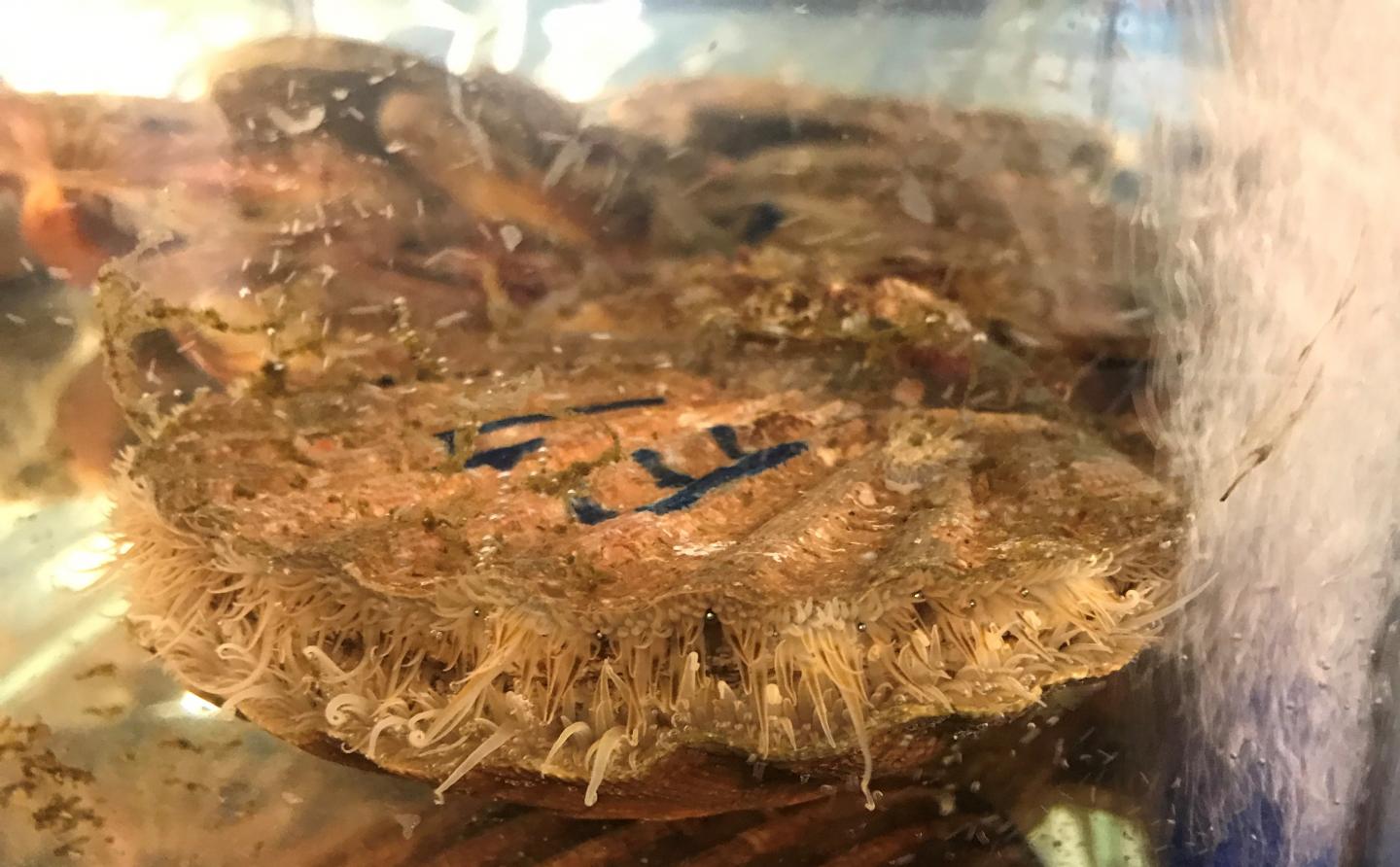
For the sake of comparison, I wish they’d thought to include an image of a giant scallop that hadn’t been used in the research (I have an ‘unplastic’ giant scallop image at the end of this posting),
Caption: These are some of the scallops used as part of the current research. Credit: University of Plymouth
But, they did do this,
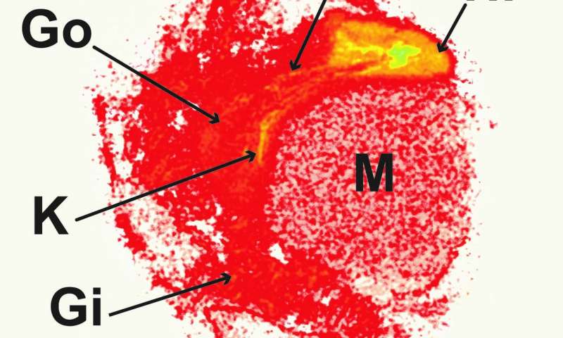
A scan showing nanoplastic particles accumulated within the scallop’s gills (GI), kidney (K), gonad (GO), intestine (I), hepatopancreas (HP) and muscle (M). Credit: University of Plymouth [downloaded from https://phys.org/news/2018-12-billions-nanoplastics-accumulate-marine-hours.html]
A ground-breaking study has shown it takes a matter of hours for billions of minute plastic nanoparticles to become embedded throughout the major organs of a marine organism.
The research, led by the University of Plymouth, examined the uptake of nanoparticles by a commercially important mollusc, the great scallop (Pecten maximus).
After six hours exposure in the laboratory, billions of particles measuring 250nm (around 0.00025mm) had accumulated within the scallop’s intestines.
However, considerably more even smaller particles measuring 20nm (0.00002mm) had become dispersed throughout the body including the kidney, gill, muscle and other organs.
The study is the first to quantify the uptake of nanoparticles at predicted environmentally relevant conditions, with previous research having been conducted at far higher concentrations than scientists believe are found in our oceans.
Dr Maya Al Sid Cheikh, Postdoctoral Research Fellow at the University of Plymouth, led the study. She said: “For this experiment, we needed to develop an entirely novel scientific approach. We made nanoparticles of plastic in our laboratories and incorporated a label so that we could trace the particles in the body of the scallop at environmentally relevant concentrations. The results of the study show for the first time that nanoparticles can be rapidly taken up by a marine organism, and that in just a few hours they become distributed across most of the major organs.”
Professor Richard Thompson OBE, Head of the University’s International Marine Litter Research Unit, added: “This is a ground breaking study, in terms of both the scientific approach and the findings. We only exposed the scallops to nanoparticles for a few hours and, despite them being transferred to clean conditions, traces were still present several weeks later. Understanding the dynamics of nanoparticle uptake and release, as well as their distribution in body tissues, is essential if we are to understand any potential effects on organisms. A key next step will be to use this approach to guide research investigating any potential effects of nanoparticles and in particular to consider the consequences of longer term exposures.”
Accepted for publication in the Environmental Science and Technology journal, the study also involved scientists from the Charles River Laboratories in Elphinstone, Scotland; the Institute Maurice la Montagne in Canada; and Heriot-Watt University.
It was conducted as part of RealRiskNano, a £1.1million project funded by the Natural Environment Research Council (NERC). Led by Heriot-Watt and Plymouth, it is exploring the effects which microscopic plastic particles can have on the marine environment.
In this study, the scallops were exposed to quantities of carbon-radiolabeled nanopolystyrene and after six hours, autoradiography was used to show the number of particles present in organs and tissue.
It was also used to demonstrate that the 20nm particles were no longer detectable after 14 days, whereas 250nm particles took 48 days to disappear.
Ted Henry, Professor of Environmental Toxicology at Heriot-Watt University, said: “Understanding whether plastic particles are absorbed across biological membranes and accumulate within internal organs is critical for assessing the risk these particles pose to both organism and human health. The novel use of radiolabelled plastic particles pioneered in Plymouth provides the most compelling evidence to date on the level of absorption of plastic particles in a marine organism.”
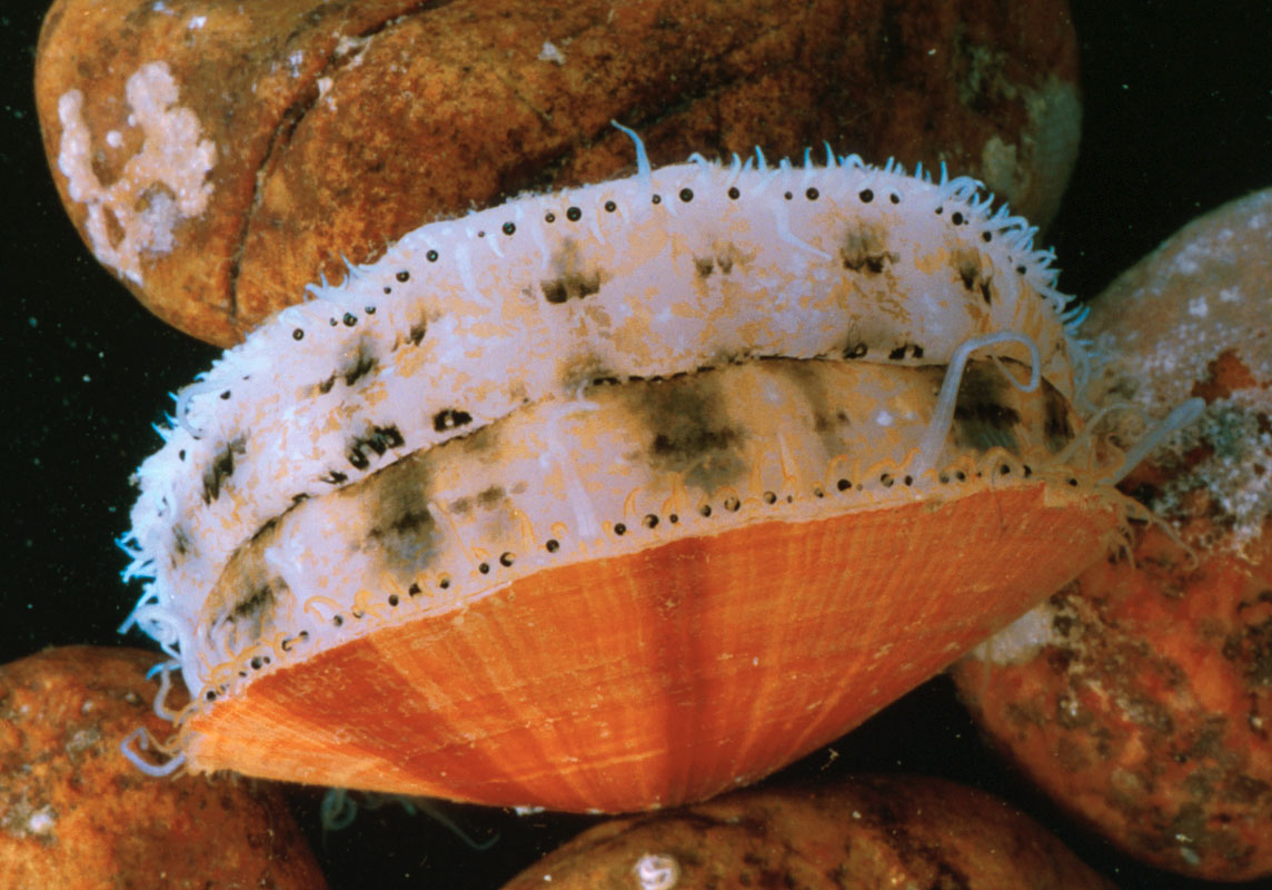
The sea scallop (Placopecten magellanicus) has over 100 blue eyes along the edge of its mantle, with which it senses light intensity. This mollusk has the ability to scoot away from potential danger by flapping the two parts of its shell, like a swimming castenet. Credit: Dann Blackwood, USGS – http://www.sanctuaries.nos.noaa.gov/pgallery/pgstellwagen/living/living_17.html Public Domain
Every time I think this CRISPR (clustered regularly interspaced short palindromic repeats) story is winding down, something new happens. The latest (I think) is in a June 3, 2019 news item on ScienceDaily,
A genetic mutation that a Chinese scientist attempted to create in twin babies born last year, ostensibly to help them fend off HIV infection, is also associated with a 21% increase in mortality in later life, according to an analysis by University of California, Berkeley, scientists.
The researchers scanned more than 400,000 genomes and associated health records contained in a British database, UK Biobank, and found that people who had two mutated copies of the gene had a significantly higher death rate between ages 41 and 78 than those with one or no copies.
Sarah Zhang’s June 3, 2019 article for The Atlantic provides an overview of the situation before exploring the current controversy,
In the 1990s, virologists in New York learned of a genetic mutation that would become one of the most famous ever discovered. They found it in a man who could not be infected with HIV. He turned out to be missing just 32 letters in a gene called CCR5, and remarkably, it was enough to make him resistant to the virus killing so many others. About 1 percent of people of European descent carry two copies of this mutation, now known as CCR5-Δ32.
In 2018, a Chinese scientist named He Jiankui made the mutation infamous when he attempted to use CRISPR to edit CCR5-Δ32 (pronounced “CCR5-delta-32”) into human embryos. He chose this mutation, he said, because the babies’ father was HIV-positive, and he wanted to make the resulting twin girls resistant to the virus. CCR5-Δ32 is also, after all, one of the most studied mutations.
He’s work immediately provoked outrage among scientists, who knew enough to know how much they did not know about the risks of altering CCR5. And now a new study suggests that CCR5-Δ32 is indeed harmful overall.
The girls’ CCR5 genes were altered, according to data He presented, but they do not exactly match the 32-letter deletion; it’s unclear whether either of them is actually resistant to HIV. Even if they were unable to get HIV, a body of research already suggested that CCR5-Δ32 made people more vulnerable to the flu and West Nile virus. A “good” mutation in the context of HIV can be “bad” in another context. No one knew, exactly, the net effect of a CCR5-Δ32 mutation.
…
For some reason, Zhang makes no mention of the possibly enhanced cognitive abilities that the twins may have as a consequence of the gene editing assuming that He Jiankui successfully edited the genes. (To my knowledge, the results and data have not been released for review by colleagues.)
Regardless, Zhang’s article provides a handy overview and update.
Previous studies have associated two mutated copies of the gene, CCR5, with a fourfold increase in the death rate after influenza infection, and the higher overall mortality rate may reflect this greater susceptibility to death from the flu. But the researchers say there could be any number of explanations, since the protein that CCR5 codes for, and which no longer works in those having the mutation in both copies of the gene, is involved in many body functions.
“Beyond the many ethical issues involved with the CRISPR babies, the fact is that, right now, with current knowledge, it is still very dangerous to try to introduce mutations without knowing the full effect of what those mutations do,” said Rasmus Nielsen, a UC Berkeley professor of integrative biology. “In this case, it is probably not a mutation that most people would want to have. You are actually, on average, worse off having it.”
“Because one gene could affect multiple traits, and because, depending on the environment, the effects of a mutation could be quite different, I think there can be many uncertainties and unknown effects in any germline editing,” said postdoctoral fellow Xinzhu “April” Wei. Wei is first author and Nielsen is senior author of a paper describing the research that will appear online on Monday, June 3, in the journal Nature Medicine.
Mutation prevents HIV infection
The gene CCR5 codes for a protein that, among other things, sits on the surface of immune cells and helps some strains of HIV, including the most common ones, to enter and infect them. Jiankui He, the Chinese scientist who last November shocked the world by announcing he had experimented with CCR5 on at least two babies, said he wanted to introduce a mutation in the gene that would prevent this. Naturally-occurring mutations that disable the protein are rare in Asians, but a mutation found in about 11% of Northern Europeans protects them against HIV infection.
The genetic mutation, ∆32 (Delta 32), refers to a missing 32-base-pair segment in the CCR5 gene. This mutation interferes with the localization on the cell surface of the protein for which CCR5 codes, thwarting HIV binding and infection. He was unable to duplicate the natural mutation, but appears to have generated a similar deletion that would also inactivate the protein. One of the twin babies reportedly had one copy of CCR5 modified by CRISPR-Cas9 gene editing, while the other baby had both copies edited.
But inactivating a protein found in all humans and most animals is likely to have negative effects, Nielsen said, especially when done to both copies of the gene — a so-called homozygous mutation
“Here is a functional protein that we know has an effect in the organism, and it is well-conserved among many different species, so it is likely that a mutation that destroys the protein is, on average, not good for you,” he said. “Otherwise, evolutionary mechanisms would have destroyed that protein a long time ago.”
After He’s experiment became public, Nielsen and Wei, who study current genetic variation to understand the origin of human, animal and plant traits, decided to investigate the effect of the CCR5-∆32 mutation using data from UK Biobank. The database houses genomic information on a half million U.K. citizens that is linked to their medical records. The genomic information is much like that acquired by Ancestry.com and 23andMe: details on nearly a million individual variations in the genetic sequence, so-called single nucleotide polymorphisms (SNPs).
Two independent measures indicated a higher mortality rate for those with two mutated genes. Fewer people than expected with two mutations enrolled in the database, indicating that they had died at a higher rate than the general population. And fewer than expected survived from ages 40 to 78.
“Both the proportions before enrollment and the survivorship after enrollment tell the same story, which is that you have lower survivability or higher mortality if you have two copies of the mutation,” Nielsen said. “There is simply a deficiency of individuals with two copies.”
Because the ∆32 mutation is relatively common in Northern Europeans, it must have been favored by natural selection at some point, Nielsen said, though probably not to protect against HIV, since the virus has circulated among humans only since the 1980s.
Wei said that some evidence links the mutation to increased survival after stroke and protection against smallpox and flaviviruses, a group that includes the dengue, Zika and West Nile viruses.
Despite these possible benefits, the potential unintended effects of creating genetic mutations, in both adult somatic cells and in embryonic, germline cells, argue for caution, the researchers said.
“I think there are a lot of things that are unknown at the current stage about genes’ functions,” Wei said. “The CRISPR technology is far too dangerous to use right now for germline editing.”
Here’s a link to and a citation for the latest paper,
For those who have an insatiable appetite for detail, there’s my November 28, 2018 posting which covers what happened when the CRISPR twins, Lulu and Nana, was first announced, along with a few updates to January 23, 2019. The May 17, 2019 posting covers the news of possible cognitive advantages for the CCR5-Δ32 gene-edited twins and explores some of the social implications.
Here’s one of the more recent efforts to create fibres that are electronic and capable of being woven into a smart textile. (Details about a previous effort can be found at the end of this post.) Now for this one, from a Dec. 3, 2018 news item on ScienceDaily,
The quest to create affordable, durable and mass-produced ‘smart textiles’ has been given fresh impetus through the use of the wonder material Graphene.
An international team of scientists, led by Professor Monica Craciun from the University of Exeter Engineering department, has pioneered a new technique to create fully electronic fibres that can be incorporated into the production of everyday clothing.
Currently, wearable electronics are achieved by essentially gluing devices to fabrics, which can mean they are too rigid and susceptible to malfunctioning.
The new research instead integrates the electronic devices into the fabric of the material, by coating electronic fibres with light-weight, durable components that will allow images to be shown directly on the fabric.
The research team believe that the discovery could revolutionise the creation of wearable electronic devices for use in a range of every day applications, as well as health monitoring, such as heart rates and blood pressure, and medical diagnostics.
The international collaborative research, which includes experts from the Centre for Graphene Science at the University of Exeter, the Universities of Aveiro and Lisbon in Portugal, and CenTexBel in Belgium, is published in the scientific journal Flexible Electronics.
Professor Craciun, co-author of the research said: “For truly wearable electronic devices to be achieved, it is vital that the components are able to be incorporated within the material, and not simply added to it.
Dr Elias Torres Alonso, Research Scientist at Graphenea and former PhD student in Professor Craciun’s team at Exeter added “This new research opens up the gateway for smart textiles to play a pivotal role in so many fields in the not-too-distant future. By weaving the graphene fibres into the fabric, we have created a new technique to all the full integration of electronics into textiles. The only limits from now are really within our own imagination.”
At just one atom thick, graphene is the thinnest substance capable of conducting electricity. It is very flexible and is one of the strongest known materials. The race has been on for scientists and engineers to adapt graphene for the use in wearable electronic devices in recent years.
This new research used existing polypropylene fibres – typically used in a host of commercial applications in the textile industry – to attach the new, graphene-based electronic fibres to create touch-sensor and light-emitting devices.
The new technique means that the fabrics can incorporate truly wearable displays without the need for electrodes, wires of additional materials.
Professor Saverio Russo, co-author and from the University of Exeter Physics department, added: “The incorporation of electronic devices on fabrics is something that scientists have tried to produce for a number of years, and is a truly game-changing advancement for modern technology.”
Dr Ana Neves, co-author and also from Exeter’s Engineering department added “The key to this new technique is that the textile fibres are flexible, comfortable and light, while being durable enough to cope with the demands of modern life.”
In 2015, an international team of scientists, including Professor Craciun, Professor Russo and Dr Ana Neves from the University of Exeter, have pioneered a new technique to embed transparent, flexible graphene electrodes into fibres commonly associated with the textile industry.
Here’s a link to and a citation for the paper,
Graphene electronic fibres with touch-sensing and light-emitting functionalities for smart textiles by Elias Torres Alonso, Daniela P. Rodrigues, Mukond Khetani, Dong-Wook Shin, Adolfo De Sanctis, Hugo Joulie, Isabel de Schrijver, Anna Baldycheva, Helena Alves, Ana I. S. Neves, Saverio Russo & Monica F. Craciun. Flexible Electronicsvolume 2, Article number: 25 (2018) DOI: https://doi.org/10.1038/s41528-018-0040-2 Published 25 September 2018
This paper is open access.
I have an earlier post about an effort to weave electronics into textiles for soldiers, from an April 5, 2012 posting,
I gather that today’s soldier (aka, warfighter) is carrying as many batteries as weapons. Apparently, the average soldier carries a couple of kilos worth of batteries and cables to keep their various pieces of equipment operational. The UK’s Centre for Defence Enterprise (part of the Ministry of Defence) has announced that this situation is about to change as a consequence of a recently funded research project with a company called Intelligent Textiles. From Bob Yirka’s April 3, 2012 news item for physorg.com,
To get rid of the cables, a company called Intelligent Textiles has come up with a type of yarn that can conduct electricity, which can be woven directly into the fabric of the uniform. And because they allow the uniform itself to become one large conductive unit, the need for multiple batteries can be eliminated as well.
…
I dug down to find more information about this UK initiative and the Intelligent Textiles company but the trail seems to end in 2015. Still, I did find a Canadian connection (for those who don’t know I’m a Canuck) and more about Intelligent Textile’s work with the British military in this Sept. 21, 2015 article by Barry Collins for alphr.com (Note: Links have been removed),
A two-person firm operating from a small workshop in Staines-upon-Thames, Intelligent Textiles has recently landed a multimillion-pound deal with the US Department of Defense, and is working with the Ministry of Defence (MoD) to bring its potentially life-saving technology to British soldiers. Not bad for a company that only a few years ago was selling novelty cushions.
Intelligent Textiles was born in 2002, almost by accident. Asha Peta Thompson, an arts student at Central Saint Martins, had been using textiles to teach children with special needs. That work led to a research grant from Brunel University, where she was part of a team tasked with creating a “talking jacket” for the disabled. The garment was designed to help cerebral palsy sufferers to communicate, by pressing a button on the jacket to say “my name is Peter”, for example, instead of having a Stephen Hawking-like communicator in front of them.
Another member of that Brunel team was engineering lecturer Dr Stan Swallow, who was providing the electronics expertise for the project. Pretty soon, the pair realised the prototype waistcoat they were working on wasn’t going to work: it was cumbersome, stuffed with wires, and difficult to manufacture. “That’s when we had the idea that we could weave tiny mechanical switches into the surface of the fabric,” said Thompson.
…
The conductive weave had several advantages over packing electronics into garments. “It reduces the amount of cables,” said Thompson. “It can be worn and it’s also washable, so it’s more durable. It doesn’t break; it can be worn next to the skin; it’s soft. It has all the qualities of a piece of fabric, so it’s a way of repackaging the electronics in a way that’s more user-friendly and more comfortable.” The key to Intelligent Textiles’ product isn’t so much the nature of the raw materials used, but the way they’re woven together. “All our patents are in how we weave the fabric,” Thompson explained. “We weave two conductive yarns to make a tiny mechanical switch that is perfectly separated or perfectly connected. We can weave an electronic circuit board into the fabric itself.”
…
Intelligent Textiles’ big break into the military market came when they met a British textiles firm that was supplying camouflage gear to the Canadian armed forces. [emphasis mine] The firm was attending an exhibition in Canada and invited the Intelligent Textiles duo to join them. “We showed a heated glove and an iPod controller,” said Thompson. “The Canadians said ‘that’s really fantastic, but all we need is power. Do you think you could weave a piece of fabric that distributes power?’ We said, ‘we’re already doing it’.”Before long it wasn’t only power that the Canadians wanted transmitted through the fabric, but data.
“The problem a soldier faces at the moment is that he’s carrying 60 AA batteries [to power all the equipment he carries],” said Thompson. “He doesn’t know what state of charge those batteries are at, and they’re incredibly heavy. He also has wires and cables running around the system. He has snag hazards – when he’s going into a firefight, he can get caught on door handles and branches, so cables are a real no-no.”
The Canadians invited the pair to speak at a NATO conference, where they were approached by military brass with more familiar accents. “It was there that we were spotted by the British MoD, who said ‘wow, this is a British technology but you’re being funded by Canada’,” said Thompson. That led to £235,000 of funding from the Centre for Defence Enterprise (CDE) – the money they needed to develop a fabric wiring system that runs all the way through the soldier’s vest, helmet and backpack.
…
There are more details about the 2015 state of affairs, textiles-wise, in a March 11, 2015 article by Richard Trenholm for CNET.com (Note: A link has been removed),
Speaking at the Wearable Technology Show here, Swallow describes IT [Intelligent Textiles]L as a textile company that “pretends to be a military company…it’s funny how you slip into these domains.”
One domain where this high-tech fabric has seen frontline action is in the Canadian military’s IAV Stryker armoured personnel carrier. ITL developed a full QWERTY keyboard in a single piece of fabric for use in the Stryker, replacing a traditional hardware keyboard that involved 100 components. Multiple components allow for repair, but ITL knits in redundancy so the fabric can “degrade gracefully”. The keyboard works the same as the traditional hardware, with the bonus that it’s less likely to fall on a soldier’s head, and with just one glaring downside: troops can no longer use it as a step for getting in and out of the vehicle.
…
An armoured car with knitted controls is one thing, but where the technology comes into its own is when used about the person. ITL has worked on vests like the JTAC, a system “for the guys who call down airstrikes” and need “extra computing oomph.” Then there’s SWIPES, a part of the US military’s Nett Warrior system — which uses a chest-mounted Samsung Galaxy Note 2 smartphone — and British military company BAE’s Broadsword system.
ITL is currently working on Spirit, a “truly wearable system” for the US Army and United States Marine Corps. It’s designed to be modular, scalable, intuitive and invisible.
…
While this isn’t an ITL product, this video about Broadsword technology from BAE does give you some idea of what wearable technology for soldiers is like,
baesystemsinc
Uploaded on Jul 8, 2014
Broadsword™ delivers groundbreaking technology to the 21st Century warfighter through interconnecting components that inductively transfer power and data via The Spine™, a revolutionary e-textile that can be inserted into any garment. This next-generation soldier system offers enhanced situational awareness when used with the BAE Systems’ Q-Warrior® see-through display.
If anyone should have the latest news about Intelligent Textile’s efforts, please do share in the comments section.
I do have one other posting about textiles and the military, which is dated May 9, 2012, but while it does reference US efforts it is not directly related to weaving electronics into solder’s (warfighter’s) gear.