*New fuel cell harnesses naturally occurring microbes to generate electricity
*Soil-powered sensors to successfully monitor soil moisture and detect touch
*New tech was robust enough to withstand drier soil conditions and flooding
*Fuel cell could replace batteries in sensors used for precision agriculture
EVANSTON, Ill. — A Northwestern University-led team of researchers has developed a new fuel cell that harvests energy from microbes living in dirt.
About the size of a standard paperback book, the completely soil-powered technology could fuel underground sensors used in precision agriculture and green infrastructure. This potentially could offer a sustainable, renewable alternative to batteries, which hold toxic, flammable chemicals that leach into the ground, are fraught with conflict-filled supply chains and contribute to the ever-growing problem of electronic waste.
To test the new fuel cell, the researchers used it to power sensors measuring soil moisture and detecting touch, a capability that could be valuable for tracking passing animals. To enable wireless communications, the researchers also equipped the soil-powered sensor with a tiny antenna to transmit data to a neighboring base station by reflecting existing radio frequency signals.
Not only did the fuel cell work in both wet and dry conditions, but its power also outlasted similar technologies by 120%.
The research will be published today (Jan. 12 [2024]) in the Proceedings of the Association for Computing Machinery on Interactive, Mobile, Wearable and Ubiquitous Technologies. The study authors also are releasing all designs, tutorials and simulation tools to the public, so others may use and build upon the research.
“The number of devices in the Internet of Things (IoT) is constantly growing,” said Northwestern alumnus Bill Yen, who led the work. “If we imagine a future with trillions of these devices, we cannot build every one of them out of lithium, heavy metals and toxins that are dangerous to the environment. We need to find alternatives that can provide low amounts of energy to power a decentralized network of devices. In a search for solutions, we looked to soil microbial fuel cells, which use special microbes to break down soil and use that low amount of energy to power sensors. As long as there is organic carbon in the soil for the microbes to break down, the fuel cell can potentially last forever.”
“These microbes are ubiquitous; they already live in soil everywhere,” said Northwestern’s George Wells, a senior author on the study. “We can use very simple engineered systems to capture their electricity. We’re not going to power entire cities with this energy. But we can capture minute amounts of energy to fuel practical, low-power applications.”
Wells is an associate professor of civil and environmental engineering at Northwestern’s McCormick School of Engineering. Now a Ph.D. student at Stanford University, Yen started this project when he was an undergraduate researcher in Wells’ laboratory.
Solutions for a dirty job
In recent years, farmers worldwide increasingly have adopted precision agriculture as a strategy to improve crop yields. The tech-driven approach relies on measuring precise levels of moisture, nutrients and contaminants in soil to make decisions that enhance crop health. This requires a widespread, dispersed network of electronic devices to continuously collect environmental data.
“If you want to put a sensor out in the wild, in a farm or in a wetland, you are constrained to putting a battery in it or harvesting solar energy,” Yen said. “Solar panels don’t work well in dirty environments because they get covered with dirt, do not work when the sun isn’t out and take up a lot of space. Batteries also are challenging because they run out of power. Farmers are not going to go around a 100-acre farm to regularly swap out batteries or dust off solar panels.”
To overcome these challenges, Wells, Yen and their collaborators wondered if they could instead harvest energy from the existing environment. “We could harvest energy from the soil that farmers are monitoring anyway,” Yen said.
‘Stymied efforts’
Making their first appearance in 1911, soil-based microbial fuel cells (MFCs) operate like a battery — with an anode, cathode and electrolyte. But instead of using chemicals to generate electricity, MFCs harvest electricity from bacteria that naturally donate electrons to nearby conductors. When these electrons flow from the anode to the cathode, it creates an electric circuit.
But in order for microbial fuel cells to operate without disruption, they need to stay hydrated and oxygenated — which is tricky when buried underground within dry dirt.
“Although MFCs have existed as a concept for more than a century, their unreliable performance and low output power have stymied efforts to make practical use of them, especially in low-moisture conditions,” Yen said.
Winning geometry
With these challenges in mind, Yen and his team embarked on a two-year journey to develop a practical, reliable soil-based MFC. His expedition included creating — and comparing — four different versions. First, the researchers collected a combined nine months of data on the performance of each design. Then, they tested their final version in an outdoor garden.
The best-performing prototype worked well in dry conditions as well as within a water-logged environment. The secret behind its success: Its geometry. Instead of using a traditional design, in which the anode and cathode are parallel to one another, the winning fuel cell leveraged a perpendicular design.
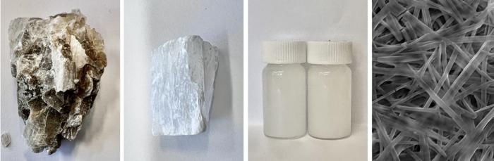
Made of carbon felt (an inexpensive, abundant conductor to capture the microbes’ electrons), the anode is horizontal to the ground’s surface. Made of an inert, conductive metal, the cathode sits vertically atop the anode.
Although the entire device is buried, the vertical design ensures that the top end is flush with the ground’s surface. A 3D-printed cap rests on top of the device to prevent debris from falling inside. And a hole on top and an empty air chamber running alongside the cathode enable consistent airflow.
The lower end of the cathode remains nestled deep beneath the surface, ensuring that it stays hydrated from the moist, surrounding soil — even when the surface soil dries out in the sunlight. The researchers also coated part of the cathode with waterproofing material to allow it to breathe during a flood. And, after a potential flood, the vertical design enables the cathode to dry out gradually rather than all at once.
On average, the resulting fuel cell generated 68 times more power than needed to operate its sensors. It also was robust enough to withstand large changes in soil moisture — from somewhat dry (41% water by volume) to completely underwater.
Making computing accessible
The researchers say all components for their soil-based MFC can be purchased at a local hardware store. Next, they plan to develop a soil-based MFC made from fully biodegradable materials. Both designs bypass complicated supply chains and avoid using conflict minerals.
“With the COVID-19 pandemic, we all became familiar with how a crisis can disrupt the global supply chain for electronics,” said study co-author Josiah Hester, a former Northwestern faculty member who is now at the Georgia Institute of Technology. “We want to build devices that use local supply chains and low-cost materials so that computing is accessible for all communities.”
The study, “Soil-powered computing: The engineer’s guide to practical soil microbial fuel cell design,” was supported by the National Science Foundation (award number CNS-2038853), the Agricultural and Food Research Initiative (award number 2023-67021-40628) from the USDA National Institute of Food and Agriculture, the Alfred P. Sloan Foundation, VMware Research and 3M.
This paper is open access.