Anyone who’s read stories about scientific discovery knows that the early stages are characterized by a number of possibilities so the current race to unseat graphene as the wonder material of the nanoworld is a ‘business as usual’ sign although I imagine it can be confusing for investors and others hoping to make their fortunes. As for the contenders to the ‘wonder nanomaterial throne’, they are transition metal dichalcogenides: molybdenum disulfide and tungsten diselenide both of which have garnered some recent attention.
A March 12, 2014 news item on Nanwerk features research on molybdenum disulfide from Poland,
Will one-atom-thick layers of molybdenum disulfide, a compound that occurs naturally in rocks, prove to be better than graphene for electronic applications? There are many signs that might prove to be the case. But physicists from the Faculty of Physics at the University of Warsaw have shown that the nature of the phenomena occurring in layered materials are still ill-understood and require further research.
….
Researchers at the University of Warsaw, Faculty of Physics (FUW) have shown that the phenomena occurring in the crystal network of molybdenum disulfide sheets are of a slightly different nature than previously thought. A report describing the discovery, achieved in collaboration with Laboratoire National des Champs Magnétiques Intenses in Grenoble, has recently been published in Applied Physics Letters.
“It will not become possible to construct complex electronic systems consisting of individual atomic sheets until we have a sufficiently good understanding of the physics involved in the phenomena occurring within the crystal network of those materials. Our research shows, however, that research still has a long way to go in this field”, says Prof. Adam Babinski at the UW Faculty of Physics.
A March 12, 2014 Dept. of Physics University of Warsaw (FUW) news release, which originated the news item, describes the researchers’ ideas about graphene and alternative materials such as molybdenum disulfide,
“It will not become possible to construct complex electronic systems consisting of individual atomic sheets until we have a sufficiently good understanding of the physics involved in the phenomena occurring within the crystal network of those materials. Our research shows, however, that research still has a long way to go in this field”, says Prof. Adam Babiński at the UW Faculty of Physics.
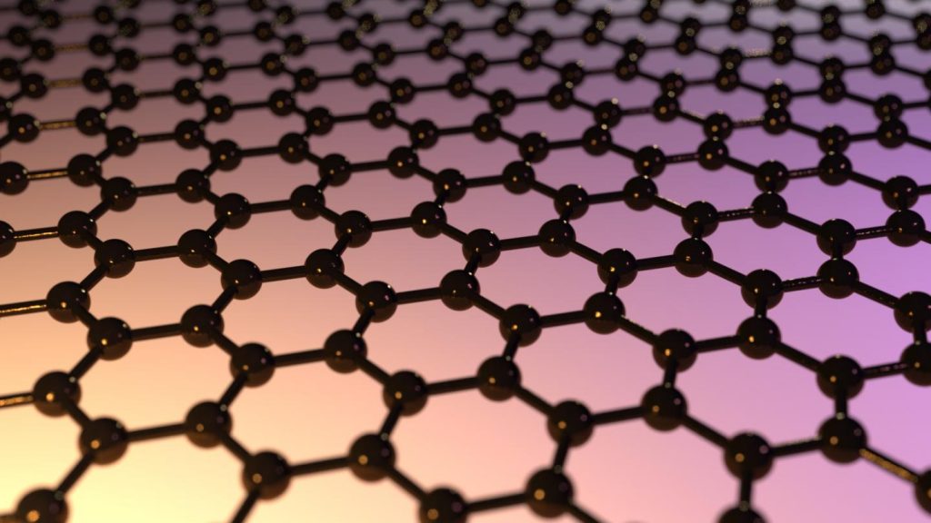
The simplest method of creating graphene is called exfoliation: a piece of scotch tape is first stuck to a piece of graphite, then peeled off. Among the particles that remain stuck to the tape, one can find microscopic layers of graphene. This is because graphite consists of many graphene sheets adjacent to one another. The carbon atoms within each layer are very strongly bound to one another (by covalent bonds, to which graphene owes its legendary resilience), but the individual layers are held together by significantly weaker bonds (van de Walls [van der Waals] bonds). Ordinary scotch tape is strong enough to break the latter and to tear individual graphene sheets away from the graphite crystal.
A few years ago it was noticed that just as graphene can be obtained from graphite, sheets a single atom thick can similarly be obtained from many other crystals. This has been successfully done, for instance, with transition metals chalcogenides (sulfides, selenides, and tellurides). Layers of molybdenum disulfide (MoS2), in particular, have proven to be a very interesting material. This compound exists in nature as molybdenite, a crystal material found in rocks around the world, frequently taking the characteristic form of silver-colored hexagonal plates. For years molybdenite has been used in the manufacturing of lubricants and metal alloys. Like in the case of graphite, the properties of single-atom sheets of MoS2 long went unnoticed.
From the standpoint of applications in electronics, molybdenum disulfide sheets exhibit a significant advantage over graphene: they have an energy gap, an energy range within which no electron states can exist. By applying electric field, the material can be switched between a state that conducts electricity and one that behaves like an insulator. By current calculations, a switched-off molybdenum disulfide transistor would consume even as little as several hundred thousand times less energy than a silicon transistor. Graphene, on the other hand, has no energy gap and transistors made of graphene cannot be fully switched off.
The news release goes on to describe how the researchers refined their understanding of molybdenum disulfide and its properties,
Valuable information about a crystal’s structure and phenomena occurring within it can be obtained by analyzing how light gets scattered within the material. Photons of a given energy are usually absorbed by the atoms and molecules of the material, then reemitted at the same energy. In the spectrum of the scattered light one can then see a distinctive peak, corresponding to that energy. It turns out, however, that one out of many millions of photons is able to use some of its energy otherwise, for instance to alter the vibration or circulation of a molecule. The reverse situation also sometimes occurs: a photon may take away some of the energy of a molecule, and so its own energy slightly increases. In this situation, known as Raman scattering, two smaller peaks are observed to either side of the main peak.
The scientists at the UW Faculty of Physics analyzed the Raman spectra of molybdenum disulfide carrying on low-temperature microscopic measurements. The higher sensitivity of the equipment and detailed analysis methods enabled the team to propose a more precise model of the phenomena occurring in the crystal network of molybdenum disulfide.
“In the case of single-layer materials, the shape of the Raman lines has previously been explained in terms of phenomena involving certain characteristic vibrations of the crystal network. We have shown for molybdenum disulfide sheets that the effects ascribed to those vibrations must actually, at least in part, be due to other network vibrations not previously taken into account”, explains Katarzyna Gołasa, a doctorate student at the UW Faculty of Physics.
The presence of the new type of vibration in single-sheet materials has an impact on how electrons behave. As a consequence, these materials must have somewhat different electronic properties than previously anticipated.
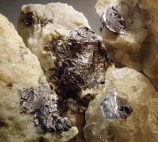
Here’s what the rocks look like,
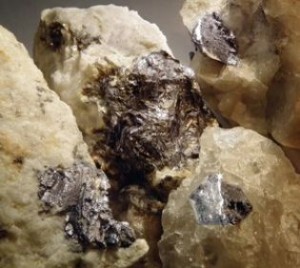
Molybdenum disulfide occurs in nature as molybdenite, crystalline material that frequently takes the characteristic form of silver-colored hexagonal plates. (Source: FUW)
I am not able to find the published research at this time (March 13, 2014).
The tungsten diselenide story is specifically application-centric. Dexter Johnson in a March 11, 2014 post on his Nanoclast blog (on the IEEE [Institute of Electrical and Electronics Engineers] website) describes the differing perspectives and potential applications suggested by the three teams that cooperated to produce papers united by a joint theme ,
The three research groups focused on optoelectronics applications of tungsten diselenide, but each with a slightly different emphasis.
The University of Washington scientists highlighted applications of the material for a light emitting diode (LED). The Vienna University of Technology group focused on the material’s photovoltaic applications. And, finally, the MIT [Massachusetts Institute of Technology] group looked at all of the optoelectronic applications for the material that would result from the way it can be switched from being a p-type to a n-type semiconductor.
Here are some details of the research from each of the institutions’ news releases.
A March 10, 2014 University of Washington (state) news release highlights their LED work,
University of Washington [UW] scientists have built the thinnest-known LED that can be used as a source of light energy in electronics. The LED is based off of two-dimensional, flexible semiconductors, making it possible to stack or use in much smaller and more diverse applications than current technology allows.
“We are able to make the thinnest-possible LEDs, only three atoms thick yet mechanically strong. Such thin and foldable LEDs are critical for future portable and integrated electronic devices,” said Xiaodong Xu, a UW assistant professor in materials science and engineering and in physics.
…
The UW’s LED is made from flat sheets of the molecular semiconductor known as tungsten diselenide, a member of a group of two-dimensional materials that have been recently identified as the thinnest-known semiconductors. Researchers use regular adhesive tape to extract a single sheet of this material from thick, layered pieces in a method inspired by the 2010 Nobel Prize in Physics awarded to the University of Manchester for isolating one-atom-thick flakes of carbon, called graphene, from a piece of graphite.
…
In addition to light-emitting applications, this technology could open doors for using light as interconnects to run nano-scale computer chips instead of standard devices that operate off the movement of electrons, or electricity. The latter process creates a lot of heat and wastes power, whereas sending light through a chip to achieve the same purpose would be highly efficient.
“A promising solution is to replace the electrical interconnect with optical ones, which will maintain the high bandwidth but consume less energy,” Xu said. “Our work makes it possible to make highly integrated and energy-efficient devices in areas such as lighting, optical communication and nano lasers.”
Here’s a link to and a citation for this team’s paper,
Electrically tunable excitonic light-emitting diodes based on monolayer WSe2 p–n junctions by Jason S. Ross, Philip Klement, Aaron M. Jones, Nirmal J. Ghimire, Jiaqiang Yan, D. G. Mandrus, Takashi Taniguchi, Kenji Watanabe, Kenji Kitamura, Wang Yao, David H. Cobden, & Xiaodong Xu. Nature Nanotechnology (2014) doi:10.1038/nnano.2014.26 Published online 09 March 2014
This paper is behind a paywall.
A March 9, 2014 University of Vienna news release highlights their work on tungsten diselinide and its possible application in solar cells,
… With graphene as a light detector, optical signals can be transformed into electric pulses on extremely short timescales.
For one very similar application, however, graphene is not well suited for building solar cells. “The electronic states in graphene are not very practical for creating photovoltaics”, says Thomas Mueller. Therefore, he and his team started to look for other materials, which, similarly to graphene, can arranged in ultrathin layers, but have even better electronic properties.
The material of choice was tungsten diselenide: It consists of one layer of tungsten atoms, which are connected by selenium atoms above and below the tungsten plane. The material absorbs light, much like graphene, but in tungsten diselenide, this light can be used to create electrical power.
The layer is so thin that 95% of the light just passes through – but a tenth of the remaining five percent, which are absorbed by the material, are converted into electrical power. Therefore, the internal efficiency is quite high. A larger portion of the incident light can be used if several of the ultrathin layers are stacked on top of each other – but sometimes the high transparency can be a useful side effect. “We are envisioning solar cell layers on glass facades, which let part of the light into the building while at the same time creating electricity”, says Thomas Mueller.
Today, standard solar cells are mostly made of silicon, they are rather bulky and inflexible. Organic materials are also used for opto-electronic applications, but they age rather quickly. “A big advantage of two-dimensional structures of single atomic layers is their crystallinity. Crystal structures lend stability”, says Thomas Mueller.
Here’s a link to and a citation for the University of Vienna paper,
Solar-energy conversion and light emission in an atomic monolayer p–n diode by Andreas Pospischil, Marco M. Furchi, & Thomas Mueller. Nature Nanotechnology (2014) doi:10.1038/nnano.2014.14 Published online 09 March 2014
This paper is behind a paywll.
Finally, a March 10, 2014 MIT news release details their work about material able to switch from p-type (p = positive) to a n-type (n = negative) semiconductors,
The material they used, called tungsten diselenide (WSe2), is part of a class of single-molecule-thick materials under investigation for possible use in new optoelectronic devices — ones that can manipulate the interactions of light and electricity. In these experiments, the MIT researchers were able to use the material to produce diodes, the basic building block of modern electronics.
Typically, diodes (which allow electrons to flow in only one direction) are made by “doping,” which is a process of injecting other atoms into the crystal structure of a host material. By using different materials for this irreversible process, it is possible to make either of the two basic kinds of semiconducting materials, p-type or n-type.
But with the new material, either p-type or n-type functions can be obtained just by bringing the vanishingly thin film into very close proximity with an adjacent metal electrode, and tuning the voltage in this electrode from positive to negative. That means the material can easily and instantly be switched from one type to the other, which is rarely the case with conventional semiconductors.
In their experiments, the MIT team produced a device with a sheet of WSe2 material that was electrically doped half n-type and half p-type, creating a working diode that has properties “very close to the ideal,” Jarillo-Herrero says.
By making diodes, it is possible to produce all three basic optoelectronic devices — photodetectors, photovoltaic cells, and LEDs; the MIT team has demonstrated all three, Jarillo-Herrero says. While these are proof-of-concept devices, and not designed for scaling up, the successful demonstration could point the way toward a wide range of potential uses, he says.
“It’s known how to make very large-area materials” of this type, Churchill says. While further work will be required, he says, “there’s no reason you wouldn’t be able to do it on an industrial scale.”
In principle, Jarillo-Herrero says, because this material can be engineered to produce different values of a key property called bandgap, it should be possible to make LEDs that produce any color — something that is difficult to do with conventional materials. And because the material is so thin, transparent, and lightweight, devices such as solar cells or displays could potentially be built into building or vehicle windows, or even incorporated into clothing, he says.
While selenium is not as abundant as silicon or other promising materials for electronics, the thinness of these sheets is a big advantage, Churchill points out: “It’s thousands or tens of thousands of times thinner” than conventional diode materials, “so you’d use thousands of times less material” to make devices of a given size.
Here’s a link to and a citation for the MIT paper,
Optoelectronic devices based on electrically tunable p–n diodes in a monolayer dichalcogenide by Britton W. H. Baugher, Hugh O. H. Churchill, Yafang Yang, & Pablo Jarillo-Herrero. Nature Nanotechnology (2014) doi:10.1038/nnano.2014.25 Published online 09 March 2014
This paper is behind a paywall.
These are very exciting, if not to say, electrifying times. (Couldn’t resist the wordplay.)