Tag Archives: boron nitride

‘Lilliputian’ skyscraper: white graphene for hydrogen storage

This story comes from Rice University (Texas, US). From a March 12, 2018 news item on Nanowerk,

Rice University engineers have zeroed in on the optimal architecture for storing hydrogen in “white graphene” nanomaterials — a design like a Lilliputian skyscraper with “floors” of boron nitride sitting one atop another and held precisely 5.2 angstroms apart by boron nitride pillars.

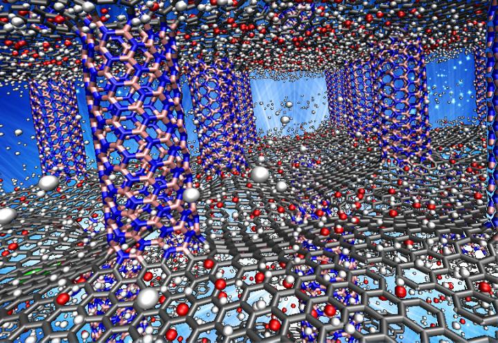
Caption Thousands of hours of calculations on Rice University’s two fastest supercomputers found that the optimal architecture for packing hydrogen into “white graphene” involves making skyscraper-like frameworks of vertical columns and one-dimensional floors that are about 5.2 angstroms apart. In this illustration, hydrogen molecules (white) sit between sheet-like floors of graphene (gray) that are supported by boron-nitride pillars (pink and blue). Researchers found that identical structures made wholly of boron-nitride had unprecedented capacity for storing readily available hydrogen. Credit Lei Tao/Rice University

A March 12, 2018 Rice University news release (also on EurekAlert), which originated the news item, goes into extensive detail about the work,

“The motivation is to create an efficient material that can take up and hold a lot of hydrogen — both by volume and weight — and that can quickly and easily release that hydrogen when it’s needed,”  [emphasis mine] said the study’s lead author, Rouzbeh Shahsavari, assistant professor of civil and environmental engineering at Rice.

Hydrogen is the lightest and most abundant element in the universe, and its energy-to-mass ratio — the amount of available energy per pound of raw material, for example — far exceeds that of fossil fuels. It’s also the cleanest way to generate electricity: The only byproduct is water. A 2017 report by market analysts at BCC Research found that global demand for hydrogen storage materials and technologies will likely reach $5.4 billion annually by 2021.

Hydrogen’s primary drawbacks relate to portability, storage and safety. While large volumes can be stored under high pressure in underground salt domes and specially designed tanks, small-scale portable tanks — the equivalent of an automobile gas tank — have so far eluded engineers.

Following months of calculations on two of Rice’s fastest supercomputers, Shahsavari and Rice graduate student Shuo Zhao found the optimal architecture for storing hydrogen in boron nitride. One form of the material, hexagonal boron nitride (hBN), consists of atom-thick sheets of boron and nitrogen and is sometimes called white graphene because the atoms are spaced exactly like carbon atoms in flat sheets of graphene.

Previous work in Shahsavari’s Multiscale Materials Lab found that hybrid materials of graphene and boron nitride could hold enough hydrogen to meet the Department of Energy’s storage targets for light-duty fuel cell vehicles.

“The choice of material is important,” he said. “Boron nitride has been shown to be better in terms of hydrogen absorption than pure graphene, carbon nanotubes or hybrids of graphene and boron nitride.

“But the spacing and arrangement of hBN sheets and pillars is also critical,” he said. “So we decided to perform an exhaustive search of all the possible geometries of hBN to see which worked best. We also expanded the calculations to include various temperatures, pressures and dopants, trace elements that can be added to the boron nitride to enhance its hydrogen storage capacity.”

Zhao and Shahsavari set up numerous “ab initio” tests, computer simulations that used first principles of physics. Shahsavari said the approach was computationally intense but worth the extra effort because it offered the most precision.

“We conducted nearly 4,000 ab initio calculations to try and find that sweet spot where the material and geometry go hand in hand and really work together to optimize hydrogen storage,” he said.

Unlike materials that store hydrogen through chemical bonding, Shahsavari said boron nitride is a sorbent that holds hydrogen through physical bonds, which are weaker than chemical bonds. That’s an advantage when it comes to getting hydrogen out of storage because sorbent materials tend to discharge more easily than their chemical cousins, Shahsavari said.

He said the choice of boron nitride sheets or tubes and the corresponding spacing between them in the superstructure were the key to maximizing capacity.

“Without pillars, the sheets sit naturally one atop the other about 3 angstroms apart, and very few hydrogen atoms can penetrate that space,” he said. “When the distance grew to 6 angstroms or more, the capacity also fell off. At 5.2 angstroms, there is a cooperative attraction from both the ceiling and floor, and the hydrogen tends to clump in the middle. Conversely, models made of purely BN tubes — not sheets — had less storage capacity.”

Shahsavari said models showed that the pure hBN tube-sheet structures could hold 8 weight percent of hydrogen. (Weight percent is a measure of concentration, similar to parts per million.) Physical experiments are needed to verify that capacity, but that the DOE’s ultimate target is 7.5 weight percent, and Shahsavari’s models suggests even more hydrogen can be stored in his structure if trace amounts of lithium are added to the hBN.

Finally, Shahsavari said, irregularities in the flat, floor-like sheets of the structure could also prove useful for engineers.

“Wrinkles form naturally in the sheets of pillared boron nitride because of the nature of the junctions between the columns and floors,” he said. “In fact, this could also be advantageous because the wrinkles can provide toughness. If the material is placed under load or impact, that buckled shape can unbuckle easily without breaking. This could add to the material’s safety, which is a big concern in hydrogen storage devices.

“Furthermore, the high thermal conductivity and flexibility of BN may provide additional opportunities to control the adsorption and release kinetics on-demand,” Shahsavari said. “For example, it may be possible to control release kinetics by applying an external voltage, heat or an electric field.”

I may be wrong but this “The motivation is to create an efficient material that can take up and hold a lot of hydrogen — both by volume and weight — and that can quickly and easily release that hydrogen when it’s needed, …”  sounds like a supercapacitor. One other comment, this research appears to be ‘in silico’, i.e., all the testing has been done as computer simulations and the proposed materials themselves have yet to be tested.

Here’s a link to and a citation for the paper,

Merger of Energetic Affinity and Optimal Geometry Provides New Class of Boron Nitride Based Sorbents with Unprecedented Hydrogen Storage Capacity by Rouzbeh Shahsavari and Shuo Zhao. Small Vol. 14 Issue 10 DOI: 10.1002/smll.201702863 Version of Record online: 8 MAR 2018

© 2018 WILEY-VCH Verlag GmbH & Co. KGaA, Weinheim

This paper is behind a paywall.

2D printed transistors in Ireland

2D transistors seem to be a hot area for research these days. In Ireland, the AMBER Centre has announced a transistor consisting entirely of 2D nanomaterials in an April 6, 2017 news item on Nanowerk,

Researchers in AMBER, the Science Foundation Ireland-funded materials science research centre hosted in Trinity College Dublin, have fabricated printed transistors consisting entirely of 2-dimensional nanomaterials for the first time. These 2D materials combine exciting electronic properties with the potential for low-cost production.

This breakthrough could unlock the potential for applications such as food packaging that displays a digital countdown to warn you of spoiling, wine labels that alert you when your white wine is at its optimum temperature, or even a window pane that shows the day’s forecast. …

An April 7, 2017 AMBER Centre press release (also on EurekAlert), which originated the news item, expands on the theme,

Prof Jonathan Coleman, who is an investigator in AMBER and Trinity’s School of Physics, said, “In the future, printed devices will be incorporated into even the most mundane objects such as labels, posters and packaging.

Printed electronic circuitry (constructed from the devices we have created) will allow consumer products to gather, process, display and transmit information: for example, milk cartons could send messages to your phone warning that the milk is about to go out-of-date.

We believe that 2D nanomaterials can compete with the materials currently used for printed electronics. Compared to other materials employed in this field, our 2D nanomaterials have the capability to yield more cost effective and higher performance printed devices. However, while the last decade has underlined the potential of 2D materials for a range of electronic applications, only the first steps have been taken to demonstrate their worth in printed electronics. This publication is important because it shows that conducting, semiconducting and insulating 2D nanomaterials can be combined together in complex devices. We felt that it was critically important to focus on printing transistors as they are the electric switches at the heart of modern computing. We believe this work opens the way to print a whole host of devices solely from 2D nanosheets.”

Led by Prof Coleman, in collaboration with the groups of Prof Georg Duesberg (AMBER) and Prof. Laurens Siebbeles (TU Delft,Netherlands), the team used standard printing techniques to combine graphene nanosheets as the electrodes with two other nanomaterials, tungsten diselenide and boron nitride as the channel and separator (two important parts of a transistor) to form an all-printed, all-nanosheet, working transistor.

Printable electronics have developed over the last thirty years based mainly on printable carbon-based molecules. While these molecules can easily be turned into printable inks, such materials are somewhat unstable and have well-known performance limitations. There have been many attempts to surpass these obstacles using alternative materials, such as carbon nanotubes or inorganic nanoparticles, but these materials have also shown limitations in either performance or in manufacturability. While the performance of printed 2D devices cannot yet compare with advanced transistors, the team believe there is a wide scope to improve performance beyond the current state-of-the-art for printed transistors.

The ability to print 2D nanomaterials is based on Prof. Coleman’s scalable method of producing 2D nanomaterials, including graphene, boron nitride, and tungsten diselenide nanosheets, in liquids, a method he has licensed to Samsung and Thomas Swan. These nanosheets are flat nanoparticles that are a few nanometres thick but hundreds of nanometres wide. Critically, nanosheets made from different materials have electronic properties that can be conducting, insulating or semiconducting and so include all the building blocks of electronics. Liquid processing is especially advantageous in that it yields large quantities of high quality 2D materials in a form that is easy to process into inks. Prof. Coleman’s publication provides the potential to print circuitry at extremely low cost which will facilitate a range of applications from animated posters to smart labels.

Prof Coleman is a partner in Graphene flagship, a €1 billion EU initiative to boost new technologies and innovation during the next 10 years.

Here’s a link to and a citation for the paper,

All-printed thin-film transistors from networks of liquid-exfoliated nanosheets by Adam G. Kelly, Toby Hallam, Claudia Backes, Andrew Harvey, Amir Sajad Esmaeily, Ian Godwin, João Coelho, Valeria Nicolosi, Jannika Lauth, Aditya Kulkarni, Sachin Kinge, Laurens D. A. Siebbeles, Georg S. Duesberg, Jonathan N. Coleman. Science  07 Apr 2017: Vol. 356, Issue 6333, pp. 69-73 DOI: 10.1126/science.aal4062

This paper is behind a paywall.

Boron nitride-graphene hybrid nanostructures could lead to next generation ‘green’ cars

An Oct. 24, 2016 phys.org news item describes research which may lead to improved fuel storage in ‘green’ cars,

Layers of graphene separated by nanotube pillars of boron nitride may be a suitable material to store hydrogen fuel in cars, according to Rice University scientists.

The Department of Energy has set benchmarks for storage materials that would make hydrogen a practical fuel for light-duty vehicles. The Rice lab of materials scientist Rouzbeh Shahsavari determined in a new computational study that pillared boron nitride and graphene could be a candidate.

An Oct. 24, 2016 Rice University news release (also on EurekAlert), which originated the news item, provides more detail (Note: Links have been removed),

Shahsavari’s lab had already determined through computer models how tough and resilient pillared graphene structures would be, and later worked boron nitride nanotubes into the mix to model a unique three-dimensional architecture. (Samples of boron nitride nanotubes seamlessly bonded to graphene have been made.)

Just as pillars in a building make space between floors for people, pillars in boron nitride graphene make space for hydrogen atoms. The challenge is to make them enter and stay in sufficient numbers and exit upon demand.

In their latest molecular dynamics simulations, the researchers found that either pillared graphene or pillared boron nitride graphene would offer abundant surface area (about 2,547 square meters per gram) with good recyclable properties under ambient conditions. Their models showed adding oxygen or lithium to the materials would make them even better at binding hydrogen.

They focused the simulations on four variants: pillared structures of boron nitride or pillared boron nitride graphene doped with either oxygen or lithium. At room temperature and in ambient pressure, oxygen-doped boron nitride graphene proved the best, holding 11.6 percent of its weight in hydrogen (its gravimetric capacity) and about 60 grams per liter (its volumetric capacity); it easily beat competing technologies like porous boron nitride, metal oxide frameworks and carbon nanotubes.

At a chilly -321 degrees Fahrenheit, the material held 14.77 percent of its weight in hydrogen.

The Department of Energy’s current target for economic storage media is the ability to store more than 5.5 percent of its weight and 40 grams per liter in hydrogen under moderate conditions. The ultimate targets are 7.5 weight percent and 70 grams per liter.

Shahsavari said hydrogen atoms adsorbed to the undoped pillared boron nitride graphene, thanks to  weak van der Waals forces. When the material was doped with oxygen, the atoms bonded strongly with the hybrid and created a better surface for incoming hydrogen, which Shahsavari said would likely be delivered under pressure and would exit when pressure is released.

“Adding oxygen to the substrate gives us good bonding because of the nature of the charges and their interactions,” he said. “Oxygen and hydrogen are known to have good chemical affinity.”

He said the polarized nature of the boron nitride where it bonds with the graphene and the electron mobility of the graphene itself make the material highly tunable for applications.

“What we’re looking for is the sweet spot,” Shahsavari said, describing the ideal conditions as a balance between the material’s surface area and weight, as well as the operating temperatures and pressures. “This is only practical through computational modeling, because we can test a lot of variations very quickly. It would take experimentalists months to do what takes us only days.”

He said the structures should be robust enough to easily surpass the Department of Energy requirement that a hydrogen fuel tank be able to withstand 1,500 charge-discharge cycles.

Shayeganfar [Farzaneh Shayeganfar], a former visiting scholar at Rice, is an instructor at Shahid Rajaee Teacher Training University in Tehran, Iran.


Caption: Simulations by Rice University scientists show that pillared graphene boron nitride may be a suitable storage medium for hydrogen-powered vehicles. Above, the pink (boron) and blue (nitrogen) pillars serve as spacers for carbon graphene sheets (gray). The researchers showed the material worked best when doped with oxygen atoms (red), which enhanced its ability to adsorb and desorb hydrogen (white). Credit: Lei Tao/Rice University

Caption: Simulations by Rice University scientists show that pillared graphene boron nitride may be a suitable storage medium for hydrogen-powered vehicles. Above, the pink (boron) and blue (nitrogen) pillars serve as spacers for carbon graphene sheets (gray). The researchers showed the material worked best when doped with oxygen atoms (red), which enhanced its ability to adsorb and desorb hydrogen (white). Credit: Lei Tao/Rice University

Here’s a link to and a citation for the paper,

Oxygen and Lithium Doped Hybrid Boron-Nitride/Carbon Networks for Hydrogen Storage by Farzaneh Shayeganfar and Rouzbeh Shahsavari. Langmuir,  DOI: 10.1021/acs.langmuir.6b02997 Publication Date (Web): October 23, 2016

Copyright © 2016 American Chemical Society

This paper is behind a paywall.

I last featured research by Shayeganfar and  Shahsavari on graphene and boron nitride in a Jan. 14, 2016 posting.

Unleashing graphene electronics potential with a trio of 2D nanomaterials

Graphene has excited a great deal of interest, especially with regard to its application in the field of electronics. However, it seems that graphene may need a little help from its friends, tantalum sulfide and boron nitride, according to a July 6, 2016 news item on ScienceDaily,

Graphene has emerged as one of the most promising two-dimensional crystals, but the future of electronics may include two other nanomaterials, according to a new study by researchers at the University of California, Riverside and the University of Georgia.

In research published Monday (July 4 [2016]) in the journal Nature Nanotechnology, the researchers described the integration of three very different two-dimensional (2D) materials to yield a simple, compact, and fast voltage-controlled oscillator (VCO) device. A VCO is an electronic oscillator whose oscillation frequency is controlled by a voltage input.

Titled “An integrated Tantalum Sulfide–Boron Nitride–Graphene Oscillator: A Charge-Density-Wave Device Operating at Room Temperature,” the paper describes the development of the first useful device that exploits the potential of charge-density waves to modulate an electrical current through a 2D material. The new technology could become an ultralow power alternative to conventional silicon-based devices, which are used in thousands of applications from computers to clocks to radios. The thin, flexible nature of the device would make it ideal for use in wearable technologies.

A July 5, 2016 University of California at Riverside (UCR) news release (also on EurekAlert) by Sarah Nightingale, which originated the news item, expands on the theme,

Graphene, a single layer of carbon atoms that exhibits exceptional electrical and thermal conductivities, shows promise as a successor to silicon-based transistors. However, its application has been limited by its inability to function as a semiconductor, which is critical for the ‘on-off’ switching operations performed by electronic components.

To overcome this shortfall, the researchers turned to another 2D nanomaterial, Tantalum Sulfide (TaS2). They showed that voltage-induced changes in the atomic structure of the ‘1T prototype’ of TaS2 enable it to function as an electrical switch at room temperature–a requirement for practical applications.

“There are many charge-density wave materials that have interesting electrical switching properties. However, most of them reveal these properties at very low temperature only. The particular polytype of TaS2 that we used can have abrupt changes in resistance above room temperature. That made a crucial difference,” said Alexander Balandin, UC presidential chair professor of electrical and computer engineering in UCR’s Bourns College of Engineering, who led the research team.

To protect the TaS2 from environmental damage, the researchers coated it with another 2D material, hexagonal boron nitrate, to prevent oxidation. By pairing the boron nitride-capped TaS2 with graphene, the team constructed a three-layer VCO that could pave the way for post-silicon electronics. In the proposed design, graphene functions as an integrated tunable load resistor, which enables precise voltage control of the current and VCO frequency. The prototype UCR devices operated at MHz frequency used in radios, and the extremely fast physical processes that define the device functionality allow for the operation frequency to increase all the way to THz.

Balandin said the integrated system is the first example of a functional voltage-controlled oscillator device comprising 2D materials that operates at room temperature.

“It is difficult to compete with silicon, which has been used and improved for the past 50 years. However, we believe our device shows a unique integration of three very different 2D materials, which utilizes the intrinsic properties of each of these materials. The device can potentially become a low-power alternative to conventional silicon technologies in many different applications,” Balandin said.

The electronic function of graphene envisioned in the proposed 2D device overcomes the problem associated with the absence of the energy band gap, which so far prevented graphene’s use as the transistor channel material. The extremely high thermal conductivity of graphene comes as an additional benefit in the device structure, by facilitating heat removal. The unique heat conduction properties of graphene were experimentally discovered and theoretically explained in 2008 by Balandin’s group at UCR. The Materials Research Society recognized this groundbreaking achievement by awarding Balandin the MRS Medal in 2013.

The Balandin group also demonstrated the first integrated graphene heat spreaders for high-power transistors and light-emitting diodes. “In those applications, graphene was used exclusively as heat conducting material. Its thermal conductivity was the main property. In the present device, we utilize both electrical and thermal conductivity of graphene,” Balandin added.

Here’s a link to and a citation for the paper,

A charge-density-wave oscillator based on an integrated tantalum disulfide–boron nitride–graphene device operating at room temperature by Guanxiong Liu, Bishwajit Debnath, Timothy R. Pope, Tina T. Salguero, Roger K. Lake, & Alexander A. Balandin. Nature Nanotechnology (2016) doi:10.1038/nnano.2016.108 Published online 04 July 2016

This paper is behind a paywall.

Light-captured energetics (harvesting light for optoelectronics)

Comparing graphene to a tiger is unusual but that’s what researcher Sanfeng Wu does—eventually—in a May 13, 2016 University of Washington news release (also on EurekAlert) about his work,

In the quest to harvest light for electronics, the focal point is the moment when photons — light particles — encounter electrons, those negatively-charged subatomic particles that form the basis of our modern electronic lives. If conditions are right when electrons and photons meet, an exchange of energy can occur. Maximizing that transfer of energy is the key to making efficient light-captured energetics possible.

“This is the ideal, but finding high efficiency is very difficult,” said University of Washington physics doctoral student Sanfeng Wu. “Researchers have been looking for materials that will let them do this — one way is to make each absorbed photon transfer all of its energy to many electrons, instead of just one electron in traditional devices.”

In traditional light-harvesting methods, energy from one photon only excites one electron or none depending on the absorber’s energy gap, transferring just a small portion of light energy into electricity. The remaining energy is lost as heat. But in a paper released May 13 in Science Advances, Wu, UW associate professor Xiaodong Xu and colleagues at four other institutions describe one promising approach to coax photons into stimulating multiple electrons. Their method exploits some surprising quantum-level interactions to give one photon multiple potential electron partners. Wu and Xu, who has appointments in the UW’s Department of Materials Science & Engineering and the Department of Physics, made this surprising discovery using graphene.

There has been intense research on graphene’s electrical properties but the researchers’ discovery adds a new property to be investigated (from the news release),

“Graphene is a substance with many exciting properties,” said Wu, the paper’s lead author. “For our purposes, it shows a very efficient interaction with light.”

Graphene is a two-dimensional hexagonal lattice of carbon atoms bonded to one another, and electrons are able to move easily within graphene. The researchers took a single layer of graphene — just one sheet of carbon atoms thick — and sandwiched it between two thin layers of a material called boron-nitride.

Boron-nitride is a material that has excited a great deal of interest in the last 12 to 18 months (from the news release),

“Boron-nitride has a lattice structure that is very similar to graphene, but has very different chemical properties,” said Wu. “Electrons do not flow easily within boron-nitride; it essentially acts as an insulator.”

Xu and Wu discovered that when the graphene layer’s lattice is aligned with the layers of boron-nitride, a type of “superlattice” is created with properties allowing efficient optoelectronics that researchers had sought. These properties rely on quantum mechanics, the occasionally baffling rules that govern interactions between all known particles of matter. Wu and Xu detected unique quantum regions within the superlattice known as Van Hove singularities.

Here’s an animated .gif illustrating the superlattice in action,

The Moire superlattice they created by aligning graphene and boron-nitride. Credit: Sanfeng Wu.

The Moire superlattice they created by aligning graphene and boron-nitride. Credit: Sanfeng Wu.

The news release goes on to describe the Van Hove singularities within the superlattice and to mention the ‘tiger’,

“These are regions of huge electron density of states, and they were not accessed in either the graphene or boron-nitride alone,” said Wu. “We only created these high electron density regions in an accessible way when both layers were aligned together.”

When Xu and Wu directed energetic photons toward the superlattice, they discovered that those Van Hove singularities were sites where one energized photon could transfer its energy to multiple electrons that are subsequently collected by electrodes— not just one electron or none with the remaining energy lost as heat. By a conservative estimate, Xu and Wu report that within this superlattice one photon could “kick” as many as five electrons to flow as current.

With the discovery of collecting multiple electrons upon the absorption of one photon, researchers may be able to create highly efficient devices that could harvest light with a large energy profit. Future work would need to uncover how to organize the excited electrons into electrical current for optimizing the energy-converting efficiency and remove some of the more cumbersome properties of their superlattice, such as the need for a magnetic field. But they believe this efficient process between photons and electrons represents major progress.

“Graphene is a tiger with great potential for optoelectronics, but locked in a cage,” said Wu. “The singularities in this superlattice are a key to unlocking that cage and releasing graphene’s potential for light harvesting application.”

H/t to a May 13, 2016 news item on phys.org.

Here’s a link to and a citation for the paper,

Multiple hot-carrier collection in photo-excited graphene Moiré superlattices by Sanfeng Wu, Lei Wang, You Lai, Wen-Yu Shan, Grant Aivazian, Xian Zhang, Takashi Taniguchi, Kenji Watanabe, Di Xiao, Cory Dean, James Hone, Zhiqiang Li, and Xiaodong Xu. Science Advances 13 May 2016: Vol. 2, no. 5, e1600002 DOI: 10.1126/sciadv.1600002

This paper is open access.

Boron nitride nanotubes muscle aside carbon nanotubes

Boron nitride has been exciting members of the scientific community most recently as an alternative to carbon. A Dec. 22, 2015 news item on ScienceDaily,

When mixed with lightweight polymers, tiny carbon tubes reinforce the material, promising lightweight and strong materials for airplanes, spaceships, cars and even sports equipment. While such carbon nanotube-polymer nanocomposites have attracted enormous interest from the materials research community, a group of scientists now has evidence that a different nanotube — made from boron nitride — could offer even more strength per unit of weight.

A Dec. 22, 2015 American Institute of Physics (AIP) news release by Catherine Meyers, which originated the news item, describes why carbon nanotubes have interested scientists and the advantages presented by boron nitride nanotubes (Note: A link has been removed),

Carbon nanotubes are legendary in their strength — at least 30 times stronger than bullet-stopping Kevlar by some estimates. When mixed with lightweight polymers such as plastics and epoxy resins, the tiny tubes reinforce the material, like the rebar in a block of concrete, promising lightweight and strong materials for airplanes, spaceships, cars and even sports equipment.

While such carbon nanotube-polymer nanocomposites have attracted enormous interest from the materials research community, a group of scientists now has evidence that a different nanotube — made from boron nitride — could offer even more strength per unit of weight. …

Boron nitride, like carbon, can form single-atom-thick sheets that are rolled into cylinders to create nanotubes. By themselves boron nitride nanotubes are almost as strong as carbon nanotubes, but their real advantage in a composite material comes from the way they stick strongly to the polymer.

“The weakest link in these nanocomposites is the interface between the polymer and the nanotubes,” said Changhong Ke, an associate professor in the mechanical engineering department at the State University of New York at Binghamton. If you break a composite, the nanotubes left sticking out have clean surfaces, as opposed to having chunks of polymer still stuck to them. The clean break indicates that the connection between the tubes and the polymer fails, Ke noted.

Plucking Nanotubes

Ke and his colleagues devised a novel way to test the strength of the nanotube-polymer link. They sandwiched boron nitride nanotubes between two thin layers of polymer, with some of the nanotubes left sticking out. They selected only the tubes that were sticking straight out of the polymer, and then welded the nanotube to the tip of a tiny cantilever beam. The team applied a force on the beam and tugged increasingly harder on the nanotube until it was ripped free of the polymer.

The researchers found that the force required to pluck out a nanotube at first increased with the nanotube length, but then plateaued. The behavior is a sign that the connection between the nanotube and the polymer is failing through a crack that forms and then spreads, Ke said.

The researchers tested two forms of polymer: epoxy and poly(methyl methacrylate), or PMMA, which is the same material used for Plexiglas. They found that the epoxy-boron nitride nanotube interface was stronger than the PMMA-nanotube interface. They also found that both polymer-boron nitride nanotube binding strengths were higher than those reported for carbon nanotubes — 35 percent higher for the PMMA interface and approximately 20 percent higher for the epoxy interface.

The Advantages of Boron Nitride Nanotubes

Boron nitride nanotubes likely bind more strongly to polymers because of the way the electrons are arranged in the molecules, Ke explained. In carbon nanotubes, all carbon atoms have equal charges in their nucleus, so the atoms share electrons equally. In boron nitride, the nitrogen atom has more protons than the boron atom, so it hogs more of the electrons in the bond. The unequal charge distribution leads to a stronger attraction between the boron nitride and the polymer molecules, as verified by molecular dynamics simulations performed by Ke’s colleagues in Dr. Xianqiao Wang’s group at the University of Georgia.

Boron nitride nanotubes also have additional advantages over carbon nanotubes, Ke said. They are more stable at high temperatures and they can better absorb neutron radiation, both advantageous properties in the extreme environment of outer space. In addition, boron nitride nanotubes are piezoelectric, which means they can generate an electric charge when stretched. This property means the material offers energy harvesting as well as sensing and actuation capabilities.

The news release does note that boron nitride nanotubes have a drawback ,

The main drawback to boron nitride nanotubes is the cost. Currently they sell for about $1,000 per gram, compared to the $10-20 per gram for carbon nanotubes, Ke said. He is optimistic that the price will come down, though, noting that carbon nanotubes were similarly expensive when they were first developed.

“I think boron nitride nanotubes are the future for making polymer composites for the aerospace industry,” he said.

Here’s a link to and a citation for the paper,

Mechanical strength of boron nitride nanotube-polymer interfaces by Xiaoming Chen, Liuyang Zhang, Cheol Park, Catharine C. Fay, Xianqiao Wang, and Changhong Ke. Appl. Phys. Lett. 107, 253105 (2015); http://dx.doi.org/10.1063/1.4936755

This paper appears to be open access.

Three teams observe graphene butterflies

It took me a few minutes to find the butterflies (visual pattern recognition is not one of my strengths) but here they are,

Caption: Graphene, combined with white graphene, forms stunning 'butterfly' images. Credit: The University of Manchester

Caption: Graphene, combined with white graphene, forms stunning ‘butterfly’ images.
Credit: The University of Manchester

The May 15, 2013 University of Manchester news release (on EurekAlert and on the University of Manchester news site) describes how the ‘butterflies’ are formed,

Writing in Nature, a large international team led Dr Roman Gorbachev from The University of Manchester shows that, when graphene placed on top of insulating boron nitride, or ‘white graphene’, the electronic properties of graphene change dramatically revealing a pattern resembling a butterfly.

The pattern is referred to as the elusive Hofstadter butterfly that has been known in theory for many decades but never before observed in experiments.

More of the science needs to be explained before moving on with the ‘butterflies’ (from the news release),

One of the most remarkable properties of graphene is its high conductivity – thousands of times higher than copper. This is due to a very special pattern created by electrons that carry electricity in graphene. The carriers are called Dirac fermions and mimic massless relativistic particles called neutrinos, studies of which usually require huge facilities such as at CERN. The possibility to address similar physics in a desk-top experiment is one of the most renowned features of graphene.

Now the Manchester scientists have found a way to create multiple clones of Dirac fermions. Graphene is placed on top of boron nitride so that graphene’s electrons can ‘feel’ individual boron and nitrogen atoms. Moving along this atomic ‘washboard’, electrons rearrange themselves once again producing multiple copies of the original Dirac fermions.

Here’s where the butterflies appear (from the news release),

The researchers can create even more clones by applying a magnetic field. The clones produce an intricate pattern; the Hofstadter butterfly. It was first predicted by mathematician Douglas Hofstadter in 1976 and, despite many dedicated experimental efforts, no more than a blurred glimpse was reported before.

In addition to the described fundamental interest, the Manchester study proves that it is possible to modify properties of atomically-thin materials by placing them on top of each other. This can be useful, for example, for graphene applications such as ultra-fast photodetectors and transistors, providing a way to tweak its incredible properties.

Coincidentally, another team has also observed the Hofstadter butterfly on a graphene substrate. From the May 16, 2013 news item on Azonano,

Two research teams at the National High Magnetic Field Laboratory (MagLab) broke through a nearly 40-year barrier recently when they observed a never-before-seen energy pattern.

“The observation of the ‘Hofstadter butterfly’ marks a real landmark in condensed matter physics and high magnetic field research,” said Greg Boebinger, director of the MagLab. “It opens a new experimental direction in materials research.”

This groundbreaking research demanded the ability to measure samples of materials at very low temperatures and very high magnetic fields, up to 35 tesla. Both of those conditions are available at the MagLab, making it an international destination for scientific exploration.

The unique periodic structure used to observe the butterfly pattern was composed of boron nitride (BN) and graphene.

The May 15, 2013 Florida State University news release by Kristin Roberts, which originated the news item, describes the two teams using the MagLab facilities for their ‘butterfly’ observations,

One research team was led by Columbia University’s Philip Kim and included researchers from City University of New York, the University of Central Florida, Tohoku University and the National Institute for Materials Science in Japan. The team’s work will be published today in the Advanced Online Publication of the journal Nature. Similar results were discovered at the MagLab by a group led by Pablo Jarillo-Herrero and Raymond Ashoori at MIT, as well as scientists from Tohoku University and the National Institute for Materials Science in Japan. Their work is expected to be published soon.

For those who just can’t get enough graphene butterflies here are citations for and links to both recently published papers (the Jarillo-Herrero/Ashoori team will be publishing their work soon).

Cloning of Dirac fermions in graphene superlattices by L. A. Ponomarenko, R. V. Gorbachev, G. L. Yu,D. C. Elias, R. Jalil, A. A. Patel, A. Mishchenko, A. S. Mayorov, C. R. Woods, J. R. Wallbank, M. Mucha-Kruczynski, B. A. Piot, M. Potemski, I. V. Grigorieva, K. S. Novoselov, F. Guinea, V. I. Fal’ko & A. K. Geim. Nature doi:10.1038/nature12187 Published online   

and,

Hofstadter’s butterfly and the fractal quantum Hall effect in moiré superlattices by C. R. Dean, L. Wang, P. Maher, C. Forsythe, F. Ghahari, Y. Gao, J. Katoch, M. Ishigami, P. Moon, M. Koshino, T. Taniguchi, K. Watanabe, K. L. Shepard, J. Hone & P. Kim. Nature (2013) doi:10.1038/nature12186 Published online 15 May 2013

Both papers are behind paywalls.

Better beer in plastic bottles

This innovation in beer bottling was developed in Ireland and I’m pretty sure the Irish have themselves braced for the humourous comments sure to follow given the legends about the Irish and beer.

Here’s more about the nanotechnology-enabled plastic beer bottles from the Sept. 18, 2012 news item on Nanowerk,

Scientists at CRANN [Centre for Research on Adaptive Nanostructures and Nanodevices], the Science Foundation Ireland-funded nanoscience institute based at Trinity College Dublin, have partnered with world-leading brewing company SABMiller on a project to increase the shelf life of bottled beer in plastic bottles. The new deal will see SABMiller invest in the project over a two year period.

Professor Jonathan Coleman and his team in CRANN are using nanoscience research methods to develop a new material that will prolong the shelf-life of beer in plastic bottles. Current plastic bottles have a relatively short shelf life, as both oxygen and carbon dioxide can permeate the plastic and diminish the flavour.

The new material, when added to plastic bottles will make them extremely impervious, meaning that oxygen cannot enter and that the carbon dioxide cannot escape, thus preserving the taste and ‘fizz’.

The Sept. 18, 2012 CRANN news release does not include many more details about the technology,

The team will exfoliate nano-sheets of boron nitride, each with a thickness of approximately 50,000 times thinner than one human hair. These nano-sheets will be mixed with plastic, which will result in a material that is extremely impervious to gas molecules. The molecules will be unable to diffuse through the material and shelf life will be increased.

As well as increasing the shelf life of the beer itself, less material is required in production, reducing cost and environmental impact.

If you are lucky enough to have a subscription or have some other access to Science magazine, you can read more about Coleman’s and his team’s work on boron nitride and thin films. Here’s the citation and abstract for the article,

Two-Dimensional Nanosheets Produced by Liquid Exfoliation of Layered Materials by Jonathan N. Coleman, Mustafa Lotya, Arlene O’Neill, Shane D. Bergin, Paul J. King, Umar Khan,  Karen Young, Alexandre Gaucher, Sukanta De, Ronan J. Smith, Igor V. Shvets, Sunil K. Arora, George Stanton, Hye-Young Kim, Kangho Lee, Gyu Tae Kim, Georg S. Duesberg, Toby Hallam, John J. Boland, Jing Jing Wang, John F. Donegan, Jaime C. Grunlan, Gregory Moriarty, Aleksey Shmeliov, Rebecca J. Nicholls, James M. Perkins, Eleanor M. Grieveson, Koenraad Theuwissen, David W. McComb, Peter D. Nellist, and Valeria Nicolosi in Science 4 February 2011: Vol. 331 no. 6017 pp. 568-571 DOI: 10.1126/science.1194975

If they could be easily exfoliated, layered materials would become a diverse source of two-dimensional crystals whose properties would be useful in applications ranging from electronics to energy storage. We show that layered compounds such as MoS2, WS2, MoSe2, MoTe2, TaSe2, NbSe2, NiTe2, BN, and Bi2Te3 can be efficiently dispersed in common solvents and can be deposited as individual flakes or formed into films. Electron microscopy strongly suggests that the material is exfoliated into individual layers. By blending this material with suspensions of other nanomaterials or polymer solutions, we can prepare hybrid dispersions or composites, which can be cast into films. We show that WS2 and MoS2 effectively reinforce polymers, whereas WS2/carbon nanotube hybrid films have high conductivity, leading to promising thermoelectric properties.

This announcement comes during Ireland’s Nanoweek 2012 (Sept. 14 – 21, 2012) which I mentioned along with other nano-themed events currently taking place in Ireland in my Sept. 14, 2012 posting.