Tag Archives: photons

Electronics begone! Enter: the light-based brainlike computing chip

At this point, it’s possible I’m wrong but I think this is the first ‘memristor’ type device (also called a neuromorphic chip) based on light rather than electronics that I’ve featured here on this blog. In other words, it’s not, technically speaking, a memristor but it does have the same properties so it is a neuromorphic chip.

Caption: The optical microchips that the researchers are working on developing are about the size of a one-cent piece. Credit: WWU Muenster – Peter Leßmann

A May 8, 2019 news item on Nanowerk announces this new approach to neuromorphic hardware (Note: A link has been removed),

Researchers from the Universities of Münster (Germany), Oxford and Exeter (both UK) have succeeded in developing a piece of hardware which could pave the way for creating computers which resemble the human brain.

The scientists produced a chip containing a network of artificial neurons that works with light and can imitate the behaviour of neurons and their synapses. The network is able to “learn” information and use this as a basis for computing and recognizing patterns. As the system functions solely with light and not with electrons, it can process data many times faster than traditional systems. …

A May 8, 2019 University of Münster press release (also on EurekAlert), which originated the news item, reveals the full story,

A technology that functions like a brain? In these times of artificial intelligence, this no longer seems so far-fetched – for example, when a mobile phone can recognise faces or languages. With more complex applications, however, computers still quickly come up against their own limitations. One of the reasons for this is that a computer traditionally has separate memory and processor units – the consequence of which is that all data have to be sent back and forth between the two. In this respect, the human brain is way ahead of even the most modern computers because it processes and stores information in the same place – in the synapses, or connections between neurons, of which there are a million-billion in the brain. An international team of researchers from the Universities of Münster (Germany), Oxford and Exeter (both UK) have now succeeded in developing a piece of hardware which could pave the way for creating computers which resemble the human brain. The scientists managed to produce a chip containing a network of artificial neurons that works with light and can imitate the behaviour of neurons and their synapses.

The researchers were able to demonstrate, that such an optical neurosynaptic network is able to “learn” information and use this as a basis for computing and recognizing patterns – just as a brain can. As the system functions solely with light and not with traditional electrons, it can process data many times faster. “This integrated photonic system is an experimental milestone,” says Prof. Wolfram Pernice from Münster University and lead partner in the study. “The approach could be used later in many different fields for evaluating patterns in large quantities of data, for example in medical diagnoses.” The study is published in the latest issue of the “Nature” journal.

The story in detail – background and method used

Most of the existing approaches relating to so-called neuromorphic networks are based on electronics, whereas optical systems – in which photons, i.e. light particles, are used – are still in their infancy. The principle which the German and British scientists have now presented works as follows: optical waveguides that can transmit light and can be fabricated into optical microchips are integrated with so-called phase-change materials – which are already found today on storage media such as re-writable DVDs. These phase-change materials are characterised by the fact that they change their optical properties dramatically, depending on whether they are crystalline – when their atoms arrange themselves in a regular fashion – or amorphous – when their atoms organise themselves in an irregular fashion. This phase-change can be triggered by light if a laser heats the material up. “Because the material reacts so strongly, and changes its properties dramatically, it is highly suitable for imitating synapses and the transfer of impulses between two neurons,” says lead author Johannes Feldmann, who carried out many of the experiments as part of his PhD thesis at the Münster University.

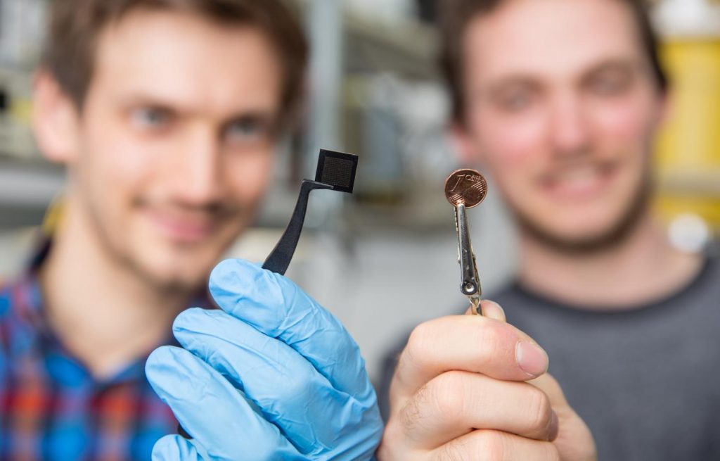
In their study, the scientists succeeded for the first time in merging many nanostructured phase-change materials into one neurosynaptic network. The researchers developed a chip with four artificial neurons and a total of 60 synapses. The structure of the chip – consisting of different layers – was based on the so-called wavelength division multiplex technology, which is a process in which light is transmitted on different channels within the optical nanocircuit.

In order to test the extent to which the system is able to recognise patterns, the researchers “fed” it with information in the form of light pulses, using two different algorithms of machine learning. In this process, an artificial system “learns” from examples and can, ultimately, generalise them. In the case of the two algorithms used – both in so-called supervised and in unsupervised learning – the artificial network was ultimately able, on the basis of given light patterns, to recognise a pattern being sought – one of which was four consecutive letters.

“Our system has enabled us to take an important step towards creating computer hardware which behaves similarly to neurons and synapses in the brain and which is also able to work on real-world tasks,” says Wolfram Pernice. “By working with photons instead of electrons we can exploit to the full the known potential of optical technologies – not only in order to transfer data, as has been the case so far, but also in order to process and store them in one place,” adds co-author Prof. Harish Bhaskaran from the University of Oxford.

A very specific example is that with the aid of such hardware cancer cells could be identified automatically. Further work will need to be done, however, before such applications become reality. The researchers need to increase the number of artificial neurons and synapses and increase the depth of neural networks. This can be done, for example, with optical chips manufactured using silicon technology. “This step is to be taken in the EU joint project ‘Fun-COMP’ by using foundry processing for the production of nanochips,” says co-author and leader of the Fun-COMP project, Prof. C. David Wright from the University of Exeter.

Here’s a link to and a citation for the paper,

All-optical spiking neurosynaptic networks with self-learning capabilities by J. Feldmann, N. Youngblood, C. D. Wright, H. Bhaskaran & W. H. P. Pernice. Nature volume 569, pages208–214 (2019) DOI: https://doi.org/10.1038/s41586-019-1157-8 Issue Date: 09 May 2019

This paper is behind a paywall.

For the curious, I found a little more information about Fun-COMP (functionally-scaled computer technology). It’s a European Commission (EC) Horizon 2020 project coordinated through the University of Exeter. For information with details such as the total cost, contribution from the EC, the list of partnerships and more there is the Fun-COMP webpage on fabiodisconzi.com.

Quantum back action and devil’s play

I always appreciate a reference to James Clerk Maxwell’s demon thought experiment (you can find out about it in the Maxwell’s demon Wikipedia entry). This time it comes from physicist  Kater Murch in a July 23, 2018 Washington University in St. Louis (WUSTL) news release (published July 25, 2018 on EurekAlert) written by Brandie Jefferson (offering a good explanation of the thought experiment and more),

Thermodynamics is one of the most human of scientific enterprises, according to Kater Murch, associate professor of physics in Arts & Sciences at Washington University in St. Louis.

“It has to do with our fascination of fire and our laziness,” he said. “How can we get fire” — or heat — “to do work for us?”

Now, Murch and colleagues have taken that most human enterprise down to the intangible quantum scale — that of ultra low temperatures and microscopic systems — and discovered that, as in the macroscopic world, it is possible to use information to extract work.

There is a catch, though: Some information may be lost in the process.

“We’ve experimentally confirmed the connection between information in the classical case and the quantum case,” Murch said, “and we’re seeing this new effect of information loss.”

The results were published in the July 20 [2018] issue of Physical Review Letters.

The international team included Eric Lutz of the University of Stuttgart; J. J. Alonzo of the University of Erlangen-Nuremberg; Alessandro Romito of Lancaster University; and Mahdi Naghiloo, a Washington University graduate research assistant in physics.

That we can get energy from information on a macroscopic scale was most famously illustrated in a thought experiment known as Maxwell’s Demon. [emphasis mine] The “demon” presides over a box filled with molecules. The box is divided in half by a wall with a door. If the demon knows the speed and direction of all of the molecules, it can open the door when a fast-moving molecule is moving from the left half of the box to the right side, allowing it to pass. It can do the same for slow particles moving in the opposite direction, opening the door when a slow-moving molecule is approaching from the right, headed left. ­

After a while, all of the quickly-moving molecules are on the right side of the box. Faster motion corresponds to higher temperature. In this way, the demon has created a temperature imbalance, where one side of the box is hotter. That temperature imbalance can be turned into work — to push on a piston as in a steam engine, for instance. At first the thought experiment seemed to show that it was possible create a temperature difference without doing any work, and since temperature differences allow you to extract work, one could build a perpetual motion machine — a violation of the second law of thermodynamics.

“Eventually, scientists realized that there’s something about the information that the demon has about the molecules,” Murch said. “It has a physical quality like heat and work and energy.”

His team wanted to know if it would be possible to use information to extract work in this way on a quantum scale, too, but not by sorting fast and slow molecules. If a particle is in an excited state, they could extract work by moving it to a ground state. (If it was in a ground state, they wouldn’t do anything and wouldn’t expend any work).

But they wanted to know what would happen if the quantum particles were in an excited state and a ground state at the same time, analogous to being fast and slow at the same time. In quantum physics, this is known as a superposition.

“Can you get work from information about a superposition of energy states?” Murch asked. “That’s what we wanted to find out.”

There’s a problem, though. On a quantum scale, getting information about particles can be a bit … tricky.

“Every time you measure the system, it changes that system,” Murch said. And if they measured the particle to find out exactly what state it was in, it would revert to one of two states: excited, or ground.

This effect is called quantum backaction. To get around it, when looking at the system, researchers (who were the “demons”) didn’t take a long, hard look at their particle. Instead, they took what was called a “weak observation.” It still influenced the state of the superposition, but not enough to move it all the way to an excited state or a ground state; it was still in a superposition of energy states. This observation was enough, though, to allow the researchers track with fairly high accuracy, exactly what superposition the particle was in — and this is important, because the way the work is extracted from the particle depends on what superposition state it is in.

To get information, even using the weak observation method, the researchers still had to take a peek at the particle, which meant they needed light. So they sent some photons in, and observed the photons that came back.

“But the demon misses some photons,” Murch said. “It only gets about half. The other half are lost.” But — and this is the key — even though the researchers didn’t see the other half of the photons, those photons still interacted with the system, which means they still had an effect on it. The researchers had no way of knowing what that effect was.

They took a weak measurement and got some information, but because of quantum backaction, they might end up knowing less than they did before the measurement. On the balance, that’s negative information.

And that’s weird.

“Do the rules of thermodynamics for a macroscopic, classical world still apply when we talk about quantum superposition?” Murch asked. “We found that yes, they hold, except there’s this weird thing. The information can be negative.

“I think this research highlights how difficult it is to build a quantum computer,” Murch said.

“For a normal computer, it just gets hot and we need to cool it. In the quantum computer you are always at risk of losing information.”

Here’s a link to and a citation for the paper,

Information Gain and Loss for a Quantum Maxwell’s Demon by M. Naghiloo, J. J. Alonso, A. Romito, E. Lutz, and K. W. Murch. Phys. Rev. Lett. 121, 030604 (Vol. 121, Iss. 3 — 20 July 2018) DOI:https://doi.org/10.1103/PhysRevLett.121.030604 Published 17 July 2018

© 2018 American Physical Society

This paper is behind a paywall.

Congratulate China on the world’s first quantum communication network

China has some exciting news about the world’s first quantum network; it’s due to open in late August 2017 so you may want to have your congratulations in order for later this month.

An Aug. 4, 2017 news item on phys.org makes the announcement,

As malicious hackers find ever more sophisticated ways to launch attacks, China is about to launch the Jinan Project, the world’s first unhackable computer network, and a major milestone in the development of quantum technology.

Named after the eastern Chinese city where the technology was developed, the network is planned to be fully operational by the end of August 2017. Jinan is the hub of the Beijing-Shanghai quantum network due to its strategic location between the two principal Chinese metropolises.

“We plan to use the network for national defence, finance and other fields, and hope to spread it out as a pilot that if successful can be used across China and the whole world,” commented Zhou Fei, assistant director of the Jinan Institute of Quantum Technology, who was speaking to Britain’s Financial Times.

An Aug. 3, 2017 CORDIS (Community Research and Development Research Information Service [for the European Commission]) press release, which originated the news item, provides more detail about the technology,

By launching the network, China will become the first country worldwide to implement quantum technology for a real life, commercial end. It also highlights that China is a key global player in the rush to develop technologies based on quantum principles, with the EU and the United States also vying for world leadership in the field.

The network, known as a Quantum Key Distribution (QKD) network, is more secure than widely used electronic communication equivalents. Unlike a conventional telephone or internet cable, which can be tapped without the sender or recipient being aware, a QKD network alerts both users to any tampering with the system as soon as it occurs. This is because tampering immediately alters the information being relayed, with the disturbance being instantly recognisable. Once fully implemented, it will make it almost impossible for other governments to listen in on Chinese communications.

In the Jinan network, some 200 users from China’s military, government, finance and electricity sectors will be able to send messages safe in the knowledge that only they are reading them. It will be the world’s longest land-based quantum communications network, stretching over 2 000 km.

Also speaking to the ‘Financial Times’, quantum physicist Tim Byrnes, based at New York University’s (NYU) Shanghai campus commented: ‘China has achieved staggering things with quantum research… It’s amazing how quickly China has gotten on with quantum research projects that would be too expensive to do elsewhere… quantum communication has been taken up by the commercial sector much more in China compared to other countries, which means it is likely to pull ahead of Europe and US in the field of quantum communication.’

However, Europe is also determined to also be at the forefront of the ‘quantum revolution’ which promises to be one of the major defining technological phenomena of the twenty-first century. The EU has invested EUR 550 million into quantum technologies and has provided policy support to researchers through the 2016 Quantum Manifesto.

Moreover, with China’s latest achievement (and a previous one already notched up from July 2017 when its quantum satellite – the world’s first – sent a message to Earth on a quantum communication channel), it looks like the race to be crowned the world’s foremost quantum power is well and truly underway…

Prior to this latest announcement, Chinese scientists had published work about quantum satellite communications, a development that makes their imminent terrestrial quantum network possible. Gabriel Popkin wrote about the quantum satellite in a June 15, 2017 article Science magazine,

Quantum entanglement—physics at its strangest—has moved out of this world and into space. In a study that shows China’s growing mastery of both the quantum world and space science, a team of physicists reports that it sent eerily intertwined quantum particles from a satellite to ground stations separated by 1200 kilometers, smashing the previous world record. The result is a stepping stone to ultrasecure communication networks and, eventually, a space-based quantum internet.

“It’s a huge, major achievement,” says Thomas Jennewein, a physicist at the University of Waterloo in Canada. “They started with this bold idea and managed to do it.”

Entanglement involves putting objects in the peculiar limbo of quantum superposition, in which an object’s quantum properties occupy multiple states at once: like Schrödinger’s cat, dead and alive at the same time. Then those quantum states are shared among multiple objects. Physicists have entangled particles such as electrons and photons, as well as larger objects such as superconducting electric circuits.

Theoretically, even if entangled objects are separated, their precarious quantum states should remain linked until one of them is measured or disturbed. That measurement instantly determines the state of the other object, no matter how far away. The idea is so counterintuitive that Albert Einstein mocked it as “spooky action at a distance.”

Starting in the 1970s, however, physicists began testing the effect over increasing distances. In 2015, the most sophisticated of these tests, which involved measuring entangled electrons 1.3 kilometers apart, showed once again that spooky action is real.

Beyond the fundamental result, such experiments also point to the possibility of hack-proof communications. Long strings of entangled photons, shared between distant locations, can be “quantum keys” that secure communications. Anyone trying to eavesdrop on a quantum-encrypted message would disrupt the shared key, alerting everyone to a compromised channel.

But entangled photons degrade rapidly as they pass through the air or optical fibers. So far, the farthest anyone has sent a quantum key is a few hundred kilometers. “Quantum repeaters” that rebroadcast quantum information could extend a network’s reach, but they aren’t yet mature. Many physicists have dreamed instead of using satellites to send quantum information through the near-vacuum of space. “Once you have satellites distributing your quantum signals throughout the globe, you’ve done it,” says Verónica Fernández Mármol, a physicist at the Spanish National Research Council in Madrid. …

Popkin goes on to detail the process for making the discovery in easily accessible (for the most part) writing and in a video and a graphic.

Russell Brandom writing for The Verge in a June 15, 2017 article about the Chinese quantum satellite adds detail about previous work and teams in other countries also working on the challenge (Note: Links have been removed),

Quantum networking has already shown promise in terrestrial fiber networks, where specialized routing equipment can perform the same trick over conventional fiber-optic cable. The first such network was a DARPA-funded connection established in 2003 between Harvard, Boston University, and a private lab. In the years since, a number of companies have tried to build more ambitious connections. The Swiss company ID Quantique has mapped out a quantum network that would connect many of North America’s largest data centers; in China, a separate team is working on a 2,000-kilometer quantum link between Beijing and Shanghai, which would rely on fiber to span an even greater distance than the satellite link. Still, the nature of fiber places strict limits on how far a single photon can travel.

According to ID Quantique, a reliable satellite link could connect the existing fiber networks into a single globe-spanning quantum network. “This proves the feasibility of quantum communications from space,” ID Quantique CEO Gregoire Ribordy tells The Verge. “The vision is that you have regional quantum key distribution networks over fiber, which can connect to each other through the satellite link.”

China isn’t the only country working on bringing quantum networks to space. A collaboration between the UK’s University of Strathclyde and the National University of Singapore is hoping to produce the same entanglement in cheap, readymade satellites called Cubesats. A Canadian team is also developing a method of producing entangled photons on the ground before sending them into space.

I wonder if there’s going to be an invitational event for scientists around the world to celebrate the launch.

Scaling up quantum dot, solar-powered windows

An Oct. 12, 2016 news item on phys.org announces that Los Alamos National Laboratory (US) may have taken a step towards scaling up quantum dot, solar-powered windows for industrial production (Note: A link has been removed),

In a paper this week for the journal Nature Energy, a Los Alamos National Laboratory research team demonstrates an important step in taking quantum dot, solar-powered windows from the laboratory to the construction site by proving that the technology can be scaled up from palm-sized demonstration models to windows large enough to put in and power a building.

“We are developing solar concentrators that will harvest sunlight from building windows and turn it into electricity, using quantum-dot based luminescent solar concentrators,” said lead scientist Victor Klimov. Klimov leads the Los Alamos Center for Advanced Solar Photophysics (CASP).

Los Alamos Center for Advanced Solar Photophysics researchers hold a large prototype solar window. From left to right: Jaehoon Lim, Kaifeng Wu, Victor Klimov, Hongbo Li.

Los Alamos Center for Advanced Solar Photophysics researchers hold a large prototype solar window. From left to right: Jaehoon Lim, Kaifeng Wu, Victor Klimov, Hongbo Li.

An Oct. 11, 2016 Los Alamos National Laboratory news release, which originated the news item, describes the work in more detail,

Luminescent solar concentrators (LSCs) are light-management devices that can serve as large-area sunlight collectors for photovoltaic cells. An LSC consists of a slab of transparent glass or plastic impregnated or coated with highly emissive fluorophores. After absorbing solar light shining onto a larger-area face of the slab, LSC fluorophores re-emit photons at a lower energy and these photons are guided by total internal reflection to the device edges where they are collected by photovoltaic cells.

At Los Alamos, researchers expand the options for energy production while minimizing the impact on the environment, supporting the Laboratory mission to strengthen energy security for the nation.

In the Nature Energy paper, the team reports on large LSC windows created using the “doctor-blade” technique for depositing thin layers of a dot/polymer composite on top of commercial large-area glass slabs. The “doctor-blade” technique comes from the world of printing and uses a blade to wipe excess liquid material such as ink from a surface, leaving a thin, highly uniform film behind. “The quantum dots used in LSC devices have been specially designed for the optimal performance as LSC fluorophores and to exhibit good compatibility with the polymer material that holds them on the surface of the window,” Klimov noted.

LSCs use colloidal quantum dots to collect light because they have properties such as widely tunable absorption and emission spectra, nearly 100 percent emission efficiencies, and high photostability (they don’t break down in sunlight).

If the cost of an LSC is much lower than that of a photovoltaic cell of comparable surface area and the LSC efficiency is sufficiently high, then it is possible to considerably reduce the cost of producing solar electricity, Klimov said. “Semitransparent LSCs can also enable new types of devices such as solar or photovoltaic windows that could turn presently passive building facades into power generation units.”

The quantum dots used in this study are semiconductor spheres with a core of one material and a shell of another. Their absorption and emission spectra can be tuned almost independently by varying the size and/or composition of the core and the shell. This allows the emission spectrum to be tuned by the parameters of the dot’s core to below the onset of strong optical absorption, which is itself tuned by the parameters of the dot’s shell. As a result, loss of light due to self-absorption is greatly reduced. “This tunability is the key property of these specially designed quantum dots that allows for record-size, high-performance LSC devices,” Klimov said.

The “LSC quantum dots” were synthesized by Jaehoon Lim (a postdoctoral research associate). Hongbo Li (postdoctoral research associate), and Kaifeng Wu (postdoctoral Director’s Fellow) developed the procedures for encapsulating quantum dots into polymer matrices and their deposition onto glass slabs by doctor-blading. Hyung-Jun Song (postdoctoral research associate) fabricated prototypes of complete LSC-solar-cell devices and characterized them.

Here’s a link to and a citation for the paper,

Doctor-blade deposition of quantum dots onto standard window glass for low-loss large-area luminescent solar concentrators by Hongbo Li, Kaifeng Wu, Jaehoon Lim, Hyung-Jun Song, & Victor I. Klimov. Nature Energy 1, Article number: 16157 (2016) doi:10.1038/nenergy.2016.157 Published online: 10 October 2016

This paper is behind a paywall.

Phenomen: a future and emerging information technology project

A Sept. 19, 2016 news item on Nanowerk describes a new research project incorporating photonics, phononics, and radio frequency signal processing,

HENOMEN is a ground breaking project designed to harness the potential of combined phononics, photonics and radio-frequency (RF) electronic signals to lay the foundations of a new information technology. This new Project, funded though the highly competitive H2020 [the European Union’s Horizon 2020 science funding programme] FET [Future and Emerging Technologies]-Open call, joins the efforts of three leading research institutes, three internationally recognised universities and a high-tech SME. The Consortium members kick-offed the project with a meeting on Friday September 16, 2016, at the Catalan Institute of Nanoscience and Nanotechnology (ICN2), coordinated by ICREA Research Prof Dr Clivia M. Sotomayor-Torres, of the ICN2’ Phononic and Photonic Nanostructures (P2N) Group.

A Sept. 16, 2016 ICN2 press release, which originated the news item, provides more detail,

Most information is currently transported by electrical charge (electrons) and by light (photons). Phonons are the quanta of lattice vibrations with frequencies covering a wide range up to tens of THz and provide coupling to the surrounding environment. In PHENOMEN the core of the research will be focused on phonon-based signal processing to enable on-chip synchronisation and transfer information carried between optical channels by phonons.

This ambitious prospect could serve as a future scalable platform for, e.g., hybrid information processing with phonons. To achieve it, PHENOMEN proposes to build the first practical optically-driven phonon sources and detectors including the engineering of phonon lasers to deliver coherent phonons to the rest of the chip pumped by a continuous wave optical source. It brings together interdisciplinary scientific and technology oriented partners in an early-stage research towards the development of a radically new technology.

The experimental implementation of phonons as information carriers in a chip is completely novel and of a clear foundational character. It deals with interaction and manipulation of fundamental particles and their intrinsic dual wave-particle character. Thus, it can only be possible with the participation of an interdisciplinary consortium which will create knowledge in a synergetic fashion and add value in the form of new theoretical tools,  develop novel methods to manipulate coherent phonons with light and build all-optical phononic circuits enabled by optomechanics.

The H2020 FET-Open call “Novel ideas for radically new technologies” aims to support the early stages of joint science and technology research for radically new future technological possibilities. The call is entirely non-prescriptive with regards to the nature or purpose of the technologies that are envisaged and thus targets mainly the unexpected. PHENOMEN is one of the 13 funded Research & Innovation Actions and went through a selection process with a success rate (1.4%) ten times smaller than that for an ERC grant. The retained proposals are expected to foster international collaboration in a multitude of disciplines such as robotics, nanotechnology, neuroscience, information science, biology, artificial intelligence or chemistry.

The Consortium

The PHENOMEN Consortium is made up by:

  • 3 leading research institutes:
  • 3 universities with an internationally recognised track-record in their respective areas of expertise:
  • 1 industrial partner:

Unbreakable encrypted message with key that’s shorter than the message

A Sept. 5, 2016 University of Rochester (NY state, US) news release (also on EurekAlert), makes an intriguing announcement,

Researchers at the University of Rochester have moved beyond the theoretical in demonstrating that an unbreakable encrypted message can be sent with a key that’s far shorter than the message—the first time that has ever been done.

Until now, unbreakable encrypted messages were transmitted via a system envisioned by American mathematician Claude Shannon, considered the “father of information theory.” Shannon combined his knowledge of algebra and electrical circuitry to come up with a binary system of transmitting messages that are secure, under three conditions: the key is random, used only once, and is at least as long as the message itself.

The findings by Daniel Lum, a graduate student in physics, and John Howell, a professor of physics, have been published in the journal Physical Review A.

“Daniel’s research amounts to an important step forward, not just for encryption, but for the field of quantum data locking,” said Howell.

Quantum data locking is a method of encryption advanced by Seth Lloyd, a professor of quantum information at Massachusetts Institute of Technology, that uses photons—the smallest particles associated with light—to carry a message. Quantum data locking was thought to have limitations for securely encrypting messages, but Lloyd figured out how to make additional assumptions—namely those involving the boundary between light and matter—to make it a more secure method of sending data.  While a binary system allows for only an on or off position with each bit of information, photon waves can be altered in many more ways: the angle of tilt can be changed, the wavelength can be made longer or shorter, and the size of the amplitude can be modified. Since a photon has more variables—and there are fundamental uncertainties when it comes to quantum measurements—the quantum key for encrypting and deciphering a message can be shorter that the message itself.

Lloyd’s system remained theoretical until this year, when Lum and his team developed a device—a quantum enigma machine—that would put the theory into practice. The device takes its name from the encryption machine used by Germany during World War II, which employed a coding method that the British and Polish intelligence agencies were secretly able to crack.

Let’s assume that Alice wants to send an encrypted message to Bob. She uses the machine to generate photons that travel through free space and into a spatial light modulator (SLM) that alters the properties of the individual photons (e.g. amplitude, tilt) to properly encode the message into flat but tilted wavefronts that can be focused to unique points dictated by the tilt. But the SLM does one more thing: it distorts the shapes of the photons into random patterns, such that the wavefront is no longer flat which means it no longer has a well-defined focus. Alice and Bob both know the keys which identify the implemented scrambling operations, so Bob is able to use his own SLM to flatten the wavefront, re-focus the photons, and translate the altered properties into the distinct elements of the message.

Along with modifying the shape of the photons, Lum and the team made use of the uncertainty principle, which states that the more we know about one property of a particle, the less we know about another of its properties. Because of that, the researchers were able to securely lock in six bits of classical information using only one bit of an encryption key—an operation called data locking.

“While our device is not 100 percent secure, due to photon loss,” said Lum, “it does show that data locking in message encryption is far more than a theory.”

The ultimate goal of the quantum enigma machine is to prevent a third party—for example, someone named Eve—from intercepting and deciphering the message. A crucial principle of quantum theory is that the mere act of measuring a quantum system changes the system. As a result, Eve has only one shot at obtaining and translating the encrypted message—something that is virtually impossible, given the nearly limitless number of patterns that exist for each photon.

The paper by Lum and Howell was one of two papers published simultaneously on the same topic. The other paper, “Quantum data locking,” was from a team led by Chinese physicist Jian-Wei Pan.

“It’s highly unlikely that our free-space implementation will be useful through atmospheric conditions,” said Lum. “Instead, we have identified the use of optic fiber as a more practical route for data locking, a path Pan’s group actually started with. Regardless, the field is still in its infancy with a great deal more research needed.”

Here’s a link to and a citation for the paper,

Quantum enigma machine: Experimentally demonstrating quantum data locking by Daniel J. Lum, John C. Howell, M. S. Allman, Thomas Gerrits, Varun B. Verma, Sae Woo Nam, Cosmo Lupo, and Seth Lloyd. Phys. Rev. A, Vol. 94, Iss. 2 — August 2016 DOI: http://dx.doi.org/10.1103/PhysRevA.94.022315

©2016 American Physical Society

This paper is behind a paywall.

There is an earlier open access version of the paper by the Chinese researchers on arXiv.org,

Experimental quantum data locking by Yang Liu, Zhu Cao, Cheng Wu, Daiji Fukuda, Lixing You, Jiaqiang Zhong, Takayuki Numata, Sijing Chen, Weijun Zhang, Sheng-Cai Shi, Chao-Yang Lu, Zhen Wang, Xiongfeng Ma, Jingyun Fan, Qiang Zhang, Jian-Wei Pan. arXiv.org > quant-ph > arXiv:1605.04030

The Chinese team’s later version of the paper is available here,

Experimental quantum data locking by Yang Liu, Zhu Cao, Cheng Wu, Daiji Fukuda, Lixing You, Jiaqiang Zhong, Takayuki Numata, Sijing Chen, Weijun Zhang, Sheng-Cai Shi, Chao-Yang Lu, Zhen Wang, Xiongfeng Ma, Jingyun Fan, Qiang Zhang, and Jian-Wei Pan. Phys. Rev. A, Vol. 94, Iss. 2 — August 2016 DOI: http://dx.doi.org/10.1103/PhysRevA.94.020301

©2016 American Physical Society

This version is behind a paywall.

Getting back to the folks at the University of Rochester, they have provided this image to illustrate their work,

The quantum enigma machine developed by researchers at the University of Rochester, MIT, and the National Institute of Standards and Technology. (Image by Daniel Lum/University of Rochester)

The quantum enigma machine developed by researchers at the University of Rochester, MIT, and the National Institute of Standards and Technology. (Image by Daniel Lum/University of Rochester)

Teleporting photons in Calgary (Canada) is a step towards a quantum internet

Scientists at the University of Calgary (Alberta, Canada) have set a distance record for the teleportation of photons and you can see the lead scientist is very pleased.

Wolfgang Tittel, professor of physics and astronomy at the University of Calgary, and a group of PhD students have developed a new quantum key distribution (QKD) system.

Wolfgang Tittel, professor of physics and astronomy at the University of Calgary, and a group of PhD students have developed a new quantum key distribution (QKD) system.

A Sept. 21, 2016 news item on phys.org makes the announcement (Note: A link has been removed),

What if you could behave like the crew on the Starship Enterprise and teleport yourself home or anywhere else in the world? As a human, you’re probably not going to realize this any time soon; if you’re a photon, you might want to keep reading.

Through a collaboration between the University of Calgary, The City of Calgary and researchers in the United States, a group of physicists led by Wolfgang Tittel, professor in the Department of Physics and Astronomy at the University of Calgary have successfully demonstrated teleportation of a photon (an elementary particle of light) over a straight-line distance of six kilometres using The City of Calgary’s fibre optic cable infrastructure. The project began with an Urban Alliance seed grant in 2014.

This accomplishment, which set a new record for distance of transferring a quantum state by teleportation, has landed the researchers a spot in the prestigious Nature Photonics scientific journal. The finding was published back-to-back with a similar demonstration by a group of Chinese researchers.

A Sept. 20, 2016 article by Robson Fletcher for CBC (Canadian Broadcasting News) online provides a bit more insight from the lead researcher (Note: A link has been removed),

“What is remarkable about this is that this information transfer happens in what we call a disembodied manner,” said physics professor Wolfgang Tittel, whose team’s work was published this week in the journal Nature Photonics.

“Our transfer happens without any need for an object to move between these two particles.”

A Sept. 20, 2016 University of Calgary news release by Drew Scherban, which originated the news item, provides more insight into the research,

“Such a network will enable secure communication without having to worry about eavesdropping, and allow distant quantum computers to connect,” says Tittel.

Experiment draws on ‘spooky action at a distance’

The experiment is based on the entanglement property of quantum mechanics, also known as “spooky action at a distance” — a property so mysterious that not even Einstein could come to terms with it.

“Being entangled means that the two photons that form an entangled pair have properties that are linked regardless of how far the two are separated,” explains Tittel. “When one of the photons was sent over to City Hall, it remained entangled with the photon that stayed at the University of Calgary.”

Next, the photon whose state was teleported to the university was generated in a third location in Calgary and then also travelled to City Hall where it met the photon that was part of the entangled pair.

“What happened is the instantaneous and disembodied transfer of the photon’s quantum state onto the remaining photon of the entangled pair, which is the one that remained six kilometres away at the university,” says Tittel.

City’s accessible dark fibre makes research possible

The research could not be possible without access to the proper technology. One of the critical pieces of infrastructure that support quantum networking is accessible dark fibre. Dark fibre, so named because of its composition — a single optical cable with no electronics or network equipment on the alignment — doesn’t interfere with quantum technology.

The City of Calgary is building and provisioning dark fibre to enable next-generation municipal services today and for the future.

“By opening The City’s dark fibre infrastructure to the private and public sector, non-profit companies, and academia, we help enable the development of projects like quantum encryption and create opportunities for further research, innovation and economic growth in Calgary,” said Tyler Andruschak, project manager with Innovation and Collaboration at The City of Calgary.

“The university receives secure access to a small portion of our fibre optic infrastructure and The City may benefit in the future by leveraging the secure encryption keys generated out of the lab’s research to protect our critical infrastructure,” said Andruschak. In order to deliver next-generation services to Calgarians, The City has been increasing its fibre optic footprint, connecting all City buildings, facilities and assets.

Timed to within one millionth of one millionth of a second

As if teleporting a photon wasn’t challenging enough, Tittel and his team encountered a number of other roadblocks along the way.

Due to changes in the outdoor temperature, the transmission time of photons from their creation point to City Hall varied over the course of a day — the time it took the researchers to gather sufficient data to support their claim. This change meant that the two photons would not meet at City Hall.

“The challenge was to keep the photons’ arrival time synchronized to within 10 pico-seconds,” says Tittel. “That is one trillionth, or one millionth of one millionth of a second.”

Secondly, parts of their lab had to be moved to two locations in the city, which as Tittel explains was particularly tricky for the measurement station at City Hall which included state-of-the-art superconducting single-photon detectors developed by the National Institute for Standards and Technology, and NASA’s Jet Propulsion Laboratory.

“Since these detectors only work at temperatures less than one degree above absolute zero the equipment also included a compact cryostat,” said Tittel.

Milestone towards a global quantum Internet

This demonstration is arguably one of the most striking manifestations of a puzzling prediction of quantum mechanics, but it also opens the path to building a future quantum internet, the long-term goal of the Tittel group.

The Urban Alliance is a strategic research partnership between The City of Calgary and University of Calgary, created in 2007 to encourage and co-ordinate the seamless transfer of cutting-edge research between the university and The City of Calgary for the benefit of all our communities. The Urban Alliance is a prime example and vehicle for one of the three foundational commitments of the University of Calgary’s Eyes High vision to fully integrate the university with the community. The City sees the Alliance as playing a key role in realizing its long-term priorities and the imagineCALGARY vision.

Here’s a link to and a citation for the paper,

Quantum teleportation across a metropolitan fibre network by Raju Valivarthi, Marcel.li Grimau Puigibert, Qiang Zhou, Gabriel H. Aguilar, Varun B. Verma, Francesco Marsili, Matthew D. Shaw, Sae Woo Nam, Daniel Oblak, & Wolfgang Tittel. Nature Photonics (2016)  doi:10.1038/nphoton.2016.180 Published online 19 September 2016

This paper is behind a paywall.

I’m 99% certain this is the paper from the Chinese researchers (referred to in the University of Calgary news release),

Quantum teleportation with independent sources and prior entanglement distribution over a network by Qi-Chao Sun, Ya-Li Mao, Si-Jing Chen, Wei Zhang, Yang-Fan Jiang, Yan-Bao Zhang, Wei-Jun Zhang, Shigehito Miki, Taro Yamashita, Hirotaka Terai, Xiao Jiang, Teng-Yun Chen, Li-Xing You, Xian-Feng Chen, Zhen Wang, Jing-Yun Fan, Qiang Zhang & Jian-Wei Pan. Nature Photonics (2016)  doi:10.1038/nphoton.2016.179 Published online 19 September 2016

This too is behind a paywall.

The science behind a hidden portrait by Edgar Degas

Rebecca Morelle’s Aug. 4, 2016 article for BBC (British Broadcasting Corporation) News online describes an intriguing piece of research into artists and how they work,

A hidden portrait by the French Impressionist painter Edgar Degas has been revealed by scientists.

Researchers in Australia used powerful X-rays to bring to light the painting of a young woman concealed beneath a work called Portrait of a Woman.

The researchers believe the subject is Emma Dobigny, who appeared in other Degas paintings.

Dr Daryl Howard, a co-author of the study, told BBC News: “I think what is really exciting is that we have now been able to add one more Degas artwork for the world to see.”

Edgar Degas, French, 1834–1917, Portrait of a Woman (Portrait de Femme), c. 1876–80, oil on canvas, 46.3 × 38.2 cm, National Gallery of Victoria, Melbourne, Felton Bequest, 1937. (a) Visible light image. The boxed region highlights the XRF scan area. (b) X-radiograph. The obscured portrait is rotated 180 degrees relative to the upper portrait. The face and ear of the obscured sitter are the primary source of contrast. (c) Reflected infrared image (detail). A partial outline of the obscured sitter’s face is indicated with a dotted line. The extensive use of highly infrared-absorbing black paint in the final composition provides a limited view of the underlying figure. Courtesy: National Gallery of Victoria, Australia

Edgar Degas, French, 1834–1917, Portrait of a Woman (Portrait de Femme), c. 1876–80, oil on canvas, 46.3 × 38.2 cm, National Gallery of Victoria, Melbourne, Felton Bequest, 1937. (a) Visible light image. The boxed region highlights the XRF scan area. (b) X-radiograph. The obscured portrait is rotated 180 degrees relative to the upper portrait. The face and ear of the obscured sitter are the primary source of contrast. (c) Reflected infrared image (detail). A partial outline of the obscured sitter’s face is indicated with a dotted line. The extensive use of highly infrared-absorbing black paint in the final composition provides a limited view of the underlying figure. Courtesy: National Gallery of Victoria, Australia

Morelle describes how the second portrait deteriorated such that a previous painting on the canvas was becoming perceptible and how scientists were able to ‘peel’ back the original to see what lay beneath,

It had long been known that Degas’ portrait of a woman wearing a black bonnet and dress, which he painted in the late 1870s, covered an earlier painting.

A ghostly impression of the composition appears as a dark stain on the sitter’s face, and over the years has become more prominent as the oil paint thinned.

Conventional X-rays revealed the outline of another image was lurking beneath, but without scraping away the outer painting, the researchers required a much more powerful technique to show any detail.

For that, they used the Australian Synchrotron, a huge accelerator that generates more powerful X-rays, to peer beneath the top layers of paint.

They were able to detect the metallic elements in the pigments that Degas had used in his underlying artwork.

Dr Howard, from the Australian Synchrotron, said: “Each element has its own unique signature, and so that gets collected.

“And what we do is analyse that data and build up these ‘elemental maps’. And that allows us to image all the different pigments used in the painting.”

Through this they were able to see in colour and in remarkable detail Degas’ hidden work: a portrait of a woman with auburn hair.

False colour reconstruction of Degas’ hidden portrait (detail). The image was created from the X-ray fluorescence microscopy elemental maps. (Edgar Degas, French, 1834–1917, Portrait of a Woman (Portrait de femme) c. 1876–80, oil on canvas, 46.3 × 38.2 cm, National Gallery of Victoria, Melbourne, Felton Bequest, 1937).

False colour reconstruction of Degas’ hidden portrait (detail). The image was created from the X-ray fluorescence microscopy elemental maps. (Edgar Degas, French, 1834–1917, Portrait of a Woman (Portrait de femme) c. 1876–80, oil on canvas, 46.3 × 38.2 cm, National Gallery of Victoria, Melbourne, Felton Bequest, 1937).

Apparently, Degas had a tendency, in his early paintings, to give his models pixie-like (longish and pointed) ears. Unusually, he has incorporated some of the features of the first painting into the second painting.

Getting back to the science, the technique used to ‘uncover’ the first painting is nondestructive (many techniques used in conservation are destructive as scrapings are required) and more powerful than previous x-ray techniques used to uncover artists’ secrets.

Here’s a link to and a citation for the paper,

A Hidden Portrait by Edgar Degas by David Thurrowgood, David Paterson, Martin D. de Jonge, Robin Kirkham, Saul Thurrowgood, & Daryl L. Howard. Scientific Reports 6, Article number: 29594 (2016) doi:10.1038/srep29594 Published online: 04 August 2016

This paper is open access but for anyone who doesn’t have the time to read it, here’s a bit from the paper’s Discussion section (Note: Links have been removed),

We are not aware of any other current analytical technique that could have achieved such an imaging outcome for this painting. The data generated by this study has provided a better understanding of the artist’s technique. The 60 μm [micrometre] spatial resolution allows us to observe with confidence that a majority of the hidden sitter’s face has been achieved as one action. However the disproportionate and blurred form of the ears is indicative of several attempts to achieve the final proportions and features. Degas is reported as having painted “pixie” like ears at about this period46. By examining single elemental maps of the painting it is possible to observe such a “pixie” like ear shape (e.g., Mn and Fe, Fig. 3) which appears to have been reworked to a more conventional form (e.g., Co and Hg, Fig. 3). Careful study of the data reveals numerous intricacies of painting technique and brush stroke direction of the underpainting. It reveals stylistic information and elemental composition information that is unlikely to be reproducible by persons attempting to copy a work, and the technique has strong potential for application in authentication studies4,5.

Consideration has been given to the properties of synchrotron radiation, and the research group used visible and chemical observation to look for radiation-induced change in preliminary experiments. Pigment binder matrices were studied by Fourier Transform Infrared (FTIR) spectroscopy before and after extended X-ray exposure at the XFM beamline, and spectroscopic changes were not detected. No evidence for any chemical or physical change was observed for radiation doses 10,000 times that reported for this study, which is in accord with recent findings by other research groups using intense radiation sources47,48.

This study has successfully demonstrated a virtual reconstruction of a hidden portrait by Edgar Degas and has delivered a better understanding of his work and artistic practices. The authors propose that the unfolding technological developments for examining artwork using synchrotron radiation-based techniques will significantly impact the ways cultural heritage is studied for authentication, preservation and scholarly purposes. We anticipate that the high quality outcome presented here and the propagation of the rapid-scanning XRF detector technology used will further stimulate growing interest in the better understanding of our cultural assets. Parallel work using portable XRF systems7 is demonstrating that a version of the technique is becoming viable (at substantially reduced spatial resolution and increased data collection time) outside of a synchrotron facility, raising a strong likelihood that precedents being set at synchrotron facilities will directly influence emerging field-based technologies. Until recently XRF large area scanning facilities were built in-house, and this had limited the technique’s availability. With the introduction of commercial large scanning area instruments on the market49, the technique has the potential to expand rapidly.

And here’s just a bit from the paper’s Methods section (Note: Links have been removed),

The scanning XRF mapping of the painting Portrait of a Woman was performed at the X-ray fluorescence microscopy (XFM) beamline of the Australian Synchrotron31. The X-ray fluorescence was acquired with the Maia 384A detector array, which integrates the sample stage motion with continuous fly scanning, leading to zero data readout overhead50,51. An incident excitation beam energy of 12.6 keV was used to circumvent intense fluorescence from the Pb L absorption edges, which would originate primarily from the painting’s Pb-based ground layer and thereby limit detection sensitivity to other elements in the pictorial paint layers. The low-energy sensitivity of the detector is limited to approximately 4 keV, thus Pb-M fluorescence (~2.3 keV) was not detectable for example. The energy resolution of the detector is 375 eV at Mn Kα.

The artwork was fitted to a custom manufactured cradle for scanning. The painting was placed approximately 13 mm from Maia detector rather than the optimal distance of 10 mm, since the painting was not perfectly flat. The painting is shown mounted at the XFM beamline in Supplementary Material Fig. S1. A 426 × 267 mm2 area was raster-scanned at 16.4 mm s−1, providing a dwell time of approximately 3.7 ms per 60 × 60 μm2 pixel and yielded a 31.6 megapixel data set in 33 h. Given the 10 × 10 μm2 incident beam size used, the average time an area of the painting was in the beam was 0.6 ms. The average incident flux on the painting was 1.5 × 109 photons s−1.

For art historians, conservationists, scientists, and people like me (the curious), this is pretty exciting stuff.

I recommend reading Morelle’s piece for anyone who finds the science a little hard going as she does an excellent job of describing the science and the art.

New form of light could lead to circuits that run on photons instead of electrons

If circuits are running on photons instead of electrons, does that mean there will be no more electricity and electronics?  Apparently, the answer is not exactly. First, an Aug. 5, 2016 news item on ScienceDaily makes the announcement about photons and circuits,

New research suggests that it is possible to create a new form of light by binding light to a single electron, combining the properties of both.

According to the scientists behind the study, from Imperial College London, the coupled light and electron would have properties that could lead to circuits that work with packages of light — photons — instead of electrons.

It would also allow researchers to study quantum physical phenomena, which govern particles smaller than atoms, on a visible scale.

An Aug. 5, 2016 Imperial College of London (ICL) press release, which originated the news item, describes the research further (Note: A link has been removed),

In normal materials, light interacts with a whole host of electrons present on the surface and within the material. But by using theoretical physics to model the behaviour of light and a recently-discovered class of materials known as topological insulators, Imperial researchers have found that it could interact with just one electron on the surface.

This would create a coupling that merges some of the properties of the light and the electron. Normally, light travels in a straight line, but when bound to the electron it would instead follow its path, tracing the surface of the material.

Improved electronics

In the study, published today in Nature Communications, Dr Vincenzo Giannini and colleagues modelled this interaction around a nanoparticle – a small sphere below 0.00000001 metres in diameter – made of a topological insulator.

Their models showed that as well as the light taking the property of the electron and circulating the particle, the electron would also take on some of the properties of the light. [emphasis mine]

Normally, as electrons are travelling along materials, such as electrical circuits, they will stop when faced with a defect. However, Dr Giannini’s team discovered that even if there were imperfections in the surface of the nanoparticle, the electron would still be able to travel onwards with the aid of the light.

If this could be adapted into photonic circuits, they would be more robust and less vulnerable to disruption and physical imperfections.

Quantum experiments

Dr Giannini said: “The results of this research will have a huge impact on the way we conceive light. Topological insulators were only discovered in the last decade, but are already providing us with new phenomena to study and new ways to explore important concepts in physics.”

Dr Giannini added that it should be possible to observe the phenomena he has modelled in experiments using current technology, and the team is working with experimental physicists to make this a reality.

He believes that the process that leads to the creation of this new form of light could be scaled up so that the phenomena could observed much more easily.

Currently, quantum phenomena can only be seen when looking at very small objects or objects that have been super-cooled, but this could allow scientists to study these kinds of behaviour at room temperature.

An electron that takes on the properties of light? I find that fascinating.

Artistic image of light trapped on the surface of a nanoparticle topological insulator. Credit: Vincenzo Giannini

Artistic image of light trapped on the surface of a nanoparticle topological insulator. Credit: Vincenzo Giannini

For those who’d like more information, here’s a link to and a citation for the paper,

Single-electron induced surface plasmons on a topological nanoparticle by G. Siroki, D.K.K. Lee, P. D. Haynes,V. Giannini. Nature Communications 7, Article number: 12375  doi:10.1038/ncomms12375 Published 05 August 2016

This paper is open access.

Pushing efficiency of perovskite-based solar cells to 31%

This atomic force microscopy image of the grainy surface of a perovskite solar cell reveals a new path to much greater efficiency. Individual grains are outlined in black, low-performing facets are red, and high-performing facets are green. A big jump in efficiency could possibly be obtained if the material can be grown so that more high-performing facets develop. (Credit: Berkeley Lab)

This atomic force microscopy image of the grainy surface of a perovskite solar cell reveals a new path to much greater efficiency. Individual grains are outlined in black, low-performing facets are red, and high-performing facets are green. A big jump in efficiency could possibly be obtained if the material can be grown so that more high-performing facets develop. (Credit: Berkeley Lab)

It’s always fascinating to observe a trend (or a craze) in science, an endeavour that outsiders (like me) tend to think of as impervious to such vagaries. Perovskite seems to be making its way past the trend/craze phase and moving into a more meaningful phase. From a July 4, 2016 news item on Nanowerk,

Scientists from the Department of Energy’s Lawrence Berkeley National Laboratory (Berkeley Lab) have discovered a possible secret to dramatically boosting the efficiency of perovskite solar cells hidden in the nanoscale peaks and valleys of the crystalline material.

Solar cells made from compounds that have the crystal structure of the mineral perovskite have captured scientists’ imaginations. They’re inexpensive and easy to fabricate, like organic solar cells. Even more intriguing, the efficiency at which perovskite solar cells convert photons to electricity has increased more rapidly than any other material to date, starting at three percent in 2009 — when researchers first began exploring the material’s photovoltaic capabilities — to 22 percent today. This is in the ballpark of the efficiency of silicon solar cells.

Now, as reported online July 4, 2016 in the journal Nature Energy (“Facet-dependent photovoltaic efficiency variations in single grains of hybrid halide perovskite”), a team of scientists from the Molecular Foundry and the Joint Center for Artificial Photosynthesis, both at Berkeley Lab, found a surprising characteristic of a perovskite solar cell that could be exploited for even higher efficiencies, possibly up to 31 percent.

A July 4, 2016 Berkeley Lab news release (also on EurekAlert), which originated the news item, details the research,

Using photoconductive atomic force microscopy, the scientists mapped two properties on the active layer of the solar cell that relate to its photovoltaic efficiency. The maps revealed a bumpy surface composed of grains about 200 nanometers in length, and each grain has multi-angled facets like the faces of a gemstone.

Unexpectedly, the scientists discovered a huge difference in energy conversion efficiency between facets on individual grains. They found poorly performing facets adjacent to highly efficient facets, with some facets approaching the material’s theoretical energy conversion limit of 31 percent.

The scientists say these top-performing facets could hold the secret to highly efficient solar cells, although more research is needed.

“If the material can be synthesized so that only very efficient facets develop, then we could see a big jump in the efficiency of perovskite solar cells, possibly approaching 31 percent,” says Sibel Leblebici, a postdoctoral researcher at the Molecular Foundry.

Leblebici works in the lab of Alexander Weber-Bargioni, who is a corresponding author of the paper that describes this research. Ian Sharp, also a corresponding author, is a Berkeley Lab scientist at the Joint Center for Artificial Photosynthesis. Other Berkeley Lab scientists who contributed include Linn Leppert, Francesca Toma, and Jeff Neaton, the director of the Molecular Foundry.

A team effort

The research started when Leblebici was searching for a new project. “I thought perovskites are the most exciting thing in solar right now, and I really wanted to see how they work at the nanoscale, which has not been widely studied,” she says.

She didn’t have to go far to find the material. For the past two years, scientists at the nearby Joint Center for Artificial Photosynthesis have been making thin films of perovskite-based compounds, and studying their ability to convert sunlight and CO2 into useful chemicals such as fuel. Switching gears, they created pervoskite solar cells composed of methylammonium lead iodide. They also analyzed the cells’ performance at the macroscale.

The scientists also made a second set of half cells that didn’t have an electrode layer. They packed eight of these cells on a thin film measuring one square centimeter. These films were analyzed at the Molecular Foundry, where researchers mapped the cells’ surface topography at a resolution of ten nanometers. They also mapped two properties that relate to the cells’ photovoltaic efficiency: photocurrent generation and open circuit voltage.

This was performed using a state-of-the-art atomic force microscopy technique, developed in collaboration with Park Systems, which utilizes a conductive tip to scan the material’s surface. The method also eliminates friction between the tip and the sample. This is important because the material is so rough and soft that friction can damage the tip and sample, and cause artifacts in the photocurrent.

Surprise discovery could lead to better solar cells

The resulting maps revealed an order of magnitude difference in photocurrent generation, and a 0.6-volt difference in open circuit voltage, between facets on the same grain. In addition, facets with high photocurrent generation had high open circuit voltage, and facets with low photocurrent generation had low open circuit voltage.

“This was a big surprise. It shows, for the first time, that perovskite solar cells exhibit facet-dependent photovoltaic efficiency,” says Weber-Bargioni.

Adds Toma, “These results open the door to exploring new ways to control the development of the material’s facets to dramatically increase efficiency.”

In practice, the facets behave like billions of tiny solar cells, all connected in parallel. As the scientists discovered, some cells operate extremely well and others very poorly. In this scenario, the current flows towards the bad cells, lowering the overall performance of the material. But if the material can be optimized so that only highly efficient facets interface with the electrode, the losses incurred by the poor facets would be eliminated.

“This means, at the macroscale, the material could possibly approach its theoretical energy conversion limit of 31 percent,” says Sharp.

A theoretical model that describes the experimental results predicts these facets should also impact the emission of light when used as an LED. …

The Molecular Foundry is a DOE Office of Science User Facility located at Berkeley Lab. The Joint Center for Artificial Photosynthesis is a DOE Energy Innovation Hub led by the California Institute of Technology in partnership with Berkeley Lab.

Here’s a link to and a citation for the paper,

Facet-dependent photovoltaic efficiency variations in single grains of hybrid halide perovskite by Sibel Y. Leblebici, Linn Leppert, Yanbo Li, Sebastian E. Reyes-Lillo, Sebastian Wickenburg, Ed Wong, Jiye Lee, Mauro Melli, Dominik Ziegler, Daniel K. Angell, D. Frank Ogletree, Paul D. Ashby, Francesca M. Toma, Jeffrey B. Neaton, Ian D. Sharp, & Alexander Weber-Bargioni. Nature Energy 1, Article number: 16093 (2016  doi:10.1038/nenergy.2016.93 Published online: 04 July 2016

This paper is behind a paywall.

Dexter Johnson’s July 6, 2016 posting on his Nanoclast blog (on the IEEE [Institute of Electrical and Electronics Engineers] website} presents his take on the impact that this new finding may have,

The rise of the crystal perovskite as a potential replacement for silicon in photovoltaics has been impressive over the last decade, with its conversion efficiency improving from 3.8 to 22.1 percent over that time period. Nonetheless, there has been a vague sense that this rise is beginning to peter out of late, largely because when a solar cell made from perovskite gets larger than 1 square centimeter the best conversion efficiency had been around 15.6 percent. …