Tag Archives: DOE

US announces fusion energy breakthrough

Nice to learn of this news, which is on the CBC (Canadian Broadcasting Corporation) news online website. From a December 13, 2022 news item provided by Associated Press (Note: the news item was updated to include general description and some Canadian content at about 12 pm PT) ,

Researchers at the Lawrence Livermore National Laboratory in California for the first time produced more energy in a fusion reaction than was used to ignite it, [emphasis mine] something called net energy gain, the Energy Department said.

Peter Behr’s December 13, 2022 article on Politico.com about the US Department of Energy’s big announcement also breaks the news,

The Department of Energy announced Tuesday [December 12, 2022] that its scientists have produced the first ever fusion reaction that yielded more energy than the reaction required, an essential step in the long path toward commercial fusion power, officials said.

The experiment Dec. 5 [2022], at the Lawrence Livermore National Laboratory in California, took a few billionths of second. But laboratory leaders said today that it demonstrated for the first time that sustained fusion power is possible.

Behr explains what nuclear fusion is but first he touches on why scientists are so interested in the process, from his December 13, 2022 article,

In theory, nuclear fusion could produce massive amounts of energy without producing lost-lasting radioactive waste, or posing the risk of meltdowns. That’s unlike nuclear fission, which powers today’s reactors.

Fission results when radioactive atoms — most commonly uranium — are split by neutrons in controlled chain reactions, creating lighter atoms and large amounts of radiation and energy to produce electric power.

Fusion is the opposite process. In the most common approach, swirling hydrogen isotopes are forced together under tremendous heat to create helium and energy for power generation. This is the same process that powers the sun and other stars. But scientists have been trying since the mid-20th century to find a way to use it to generate power on Earth.

There are two main approaches to making fusion happen and I found a description for them in an October 2022 article about local company, General Fusion, by Nelson Bennett for Business in Vancouver magazine (paper version),

Most fusion companies are pursuing one of two approaches: Magnet [sic] or inertial confinement. General fusion is one of the few that is taking a more hybrid approach ¬ magnetic confinement with pulse compression.

Fusion occurs when smaller nuclei are fused together under tremendous force into larger nuclei, with a release of energy occurring in the form of neutrons. It’s what happens to stars when gravitational force creates extreme heat that turns on the fusion engine.

Replicating that in a machine requires some form of confinement to squeeze plasma ¬ a kind of super-hot fog of unbound positive and negative particles ¬ to the point where nuclei fuse.

One approach is inertial confinement, in which lasers are focused on a small capsule of heavy hydrogen fuel (deuterium and tritium) to create ignition. This takes a tremendous amount of energy, and the challenge for all fusion efforts is to get a sustained ignition that produces more energy than it takes to get ignition ¬ called net energy gain.

The other main approach is magnetic confinement, using powerful magnets in a machine called a tokomak to contain and squeeze plasma into a donut-shaped form called a torus.

General Fusion uses magnets to confine the plasma, but to get ignition it uses pistons arrayed around a spherical chamber to fire synchronously to essentially collapse the plasma on itself and spark ignition.

General Fusion’s machine uses liquid metal spinning inside a chamber that acts as a protective barrier between the hot plasma and the machine ¬ basically a sphere of plasma contained within a sphere of liquid metal. This protects the machine from damage.

The temperatures generated in fusion ¬ up to to 150 million degrees Celsius ¬ are five to six times hotter than the core of the sun, and can destroy machines that produce them. This makes durability a big challenge in any machine.

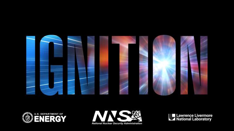
The Lawrence Livermore National Laboratory (LLNL) issued a December 13, 2022 news release, which provides more detail about their pioneering work, Note: I have changed the order of the paragraphs but all of this is from the news release,

Fusion is the process by which two light nuclei combine to form a single heavier nucleus, releasing a large amount of energy. In the 1960s, a group of pioneering scientists at LLNL hypothesized that lasers could be used to induce fusion in a laboratory setting. Led by physicist John Nuckolls, who later served as LLNL director from 1988 to 1994, this revolutionary idea became inertial confinement fusion, kicking off more than 60 years of research and development in lasers, optics, diagnostics, target fabrication, computer modeling and simulation and experimental design.

To pursue this concept, LLNL built a series of increasingly powerful laser systems, leading to the creation of NIF [National Ignition Facility], the world’s largest and most energetic laser system. NIF — located at LLNL in Livermore, California — is the size of a sports stadium and uses powerful laser beams to create temperatures and pressures like those in the cores of stars and giant planets, and inside exploding nuclear weapons.

LLNL’s experiment surpassed the fusion threshold by delivering 2.05 megajoules (MJ) of energy to the target, resulting in 3.15 MJ of fusion energy output, demonstrating for the first time a most fundamental science basis for inertial fusion energy (IFE). Many advanced science and technology developments are still needed to achieve simple, affordable IFE to power homes and businesses, and DOE is currently restarting a broad-based, coordinated IFE program in the United States. Combined with private-sector investment, there is a lot of momentum to drive rapid progress toward fusion commercialization.

If you want to see some really excited comments from scientists just read the LLNL’s December 13, 2022 news release. Even the news release’s banner is exuberant,

Behr peers into the future of fusion energy, from his December 13, 2022 article,

Fearful that China might wind up dominating fusion energy in the second half of this century, Congress in 2020 told DOE [Department of Energy] to begin funding development of a utility-scale fusion pilot plant that could deliver at least 50 megawatts of power to the U.S. grid.

In September [2022], DOE invited private companies to apply for an initial $50 million in research grants to help fund development of detailed pilot plant plans.

“We’re seeking strong partnerships between DOE and the private sector,” a senior DOE official told POLITICO’s E&E News recently. The official was not willing to speak on the record, saying the grant process is ongoing and confidential.

As the competition proceeds, DOE will set technical milestones or requirements, challenging the teams to show how critical engineering challenges will be overcome. DOE’s goal is “hopefully to enable a fusion pilot to operate in the early 2030s,” the official added.

At least 15 U.S. and foreign fusion companies have submitted requests for an initial total of $50 million in pilot plant grants, and some of them are pursuing the laser-ignition fusion process that Lawrence Livermore has pioneered, said Holland. He did not name the companies because the competition is confidential.

I wonder if General Fusion whose CEO (Chief Executive Officer) Greg Twinney declared, “Commercializing fusion energy is within reach, and General Fusion is ready to deliver it to the grid by the 2030s …” (in a December 12, 2022 company press release) is part of the US competition.

I noticed that General Fusion lists this at the end of the press release,

… Founded in 2002, we are headquartered in Vancouver, Canada, with additional centers co-located with internationally recognized fusion research laboratories near London, U.K., and Oak Ridge, Tennessee, U.S.A.

The Oak Ridge National Laboratory (ORNL), like the LLNL, is a US Department of Energy research facility.

As for General Fusion’s London connection, I have more about that in my October 28, 2022 posting “Overview of fusion energy scene,” which includes General Fusion’s then latest news about a commercialization agreement with the UKAEA (UK Atomic Energy Authority) and a ‘fusion’ video by rapper Baba Brinkman along with the overview.

Preventing corrosion in oil pipelines at the nanoscale

A June 7, 2019 news item on Azonano announces research into the process of oil pipeline corrosion at the nanoscale (Note: A link has been removed),

Steel pipes tend to rust and sooner or later fail. To anticipate disasters, oil companies and others have developed computer models to foretell when replacement is necessary. However, if the models themselves are incorrect, they can be amended only through experience, an expensive problem if detection happens too late.

Currently, scientists at Sandia National Laboratories, the Department of Energy’s Center for Integrated Nanotechnologies and the Aramco Research Center in Boston, have discovered that a specific form of nanoscale corrosion is responsible for suddenly diminishing the working life of steel pipes, according to a paper recently published in Nature’s Materials Degradation journal.

A June 6, 2019 Sandia National Laboratories news release (also on EurekAlert), which originated the news item, provides more technical detail,

Using transmission electron microscopes, which shoot electrons through targets to take pictures, the researchers were able to pin the root of the problem on a triple junction formed by a grain of cementite — a compound of carbon and iron — and two grains of ferrite, a type of iron. This junction forms frequently during most methods of fashioning steel pipe.

Iron atoms slip-sliding away

The researchers found that disorder in the atomic structure of those triple junctions made it easier for the corrosive solution to remove iron atoms along that interface.
In the experiment, the corrosive process stopped when the triple junction had been consumed by corrosion, but the crevice left behind allowed the corrosive solution to attack the interior of the steel.

“We thought of a possible solution for forming new pipe, based on changing the microstructure of the steel surface during forging, but it still needs to be tested and have a patent filed if it works,” said Sandia’s principle investigator Katherine Jungjohann, a paper author and lead microscopist. “But now we think we know where the major problem is.”

Aramco senior research scientist Steven Hayden added, “This was the world’s first real-time observation of nanoscale corrosion in a real-world material — carbon steel — which is the most prevalent type of steel used in infrastructure worldwide. Through it, we identified the types of interfaces and mechanisms that play a role in the initiation and progression of localized steel corrosion. The work is already being translated into models used to prevent corrosion-related catastrophes like infrastructure collapse and pipeline breaks.”

To mimic the chemical exposure of pipe in the field, where the expensive, delicate microscopes could not be moved, very thin pipe samples were exposed at Sandia to a variety of chemicals known to pass through oil pipelines.

Sandia researcher and paper author Khalid Hattar put a dry sample in a vacuum and used a transmission electron microscope to create maps of the steel grain types and their orientation, much as a pilot in a plane might use a camera to create area maps of farmland and roads, except that Hattar’s maps had approximately 6 nanometers resolution. (A nanometer is one-billionth of a meter.)

“By comparing these maps before and after the liquid corrosion experiments, a direct identification of the first phase that fell out of the samples could be identified, essentially identifying the weakest link in the internal microstructure,” Hattar said.

Sandia researcher and paper author Paul Kotula said, “The sample we analyzed was considered a low-carbon steel, but it has relatively high-carbon inclusions of cementite which are the sites of localized corrosion attacks.

“Our transmission electron microscopes were a key piece of this work, allowing us to image the sample, observe the corrosion process, and do microanalysis before and after the corrosion occurred to identify the part played by the ferrite and cementite grains and the corrosion product.”

When Hayden first started working in corrosion research, he said, “I was daunted at how complex and poorly understood corrosion is. This is largely because realistic experiments would involve observing complex materials like steel in liquid environments and with nanoscale resolution, and the technology to accomplish such a feat had only recently been developed and yet to be applied to corrosion. Now we are optimistic that further work at Sandia and the Center for Integrated Nanotechnologies will allow us to rethink manufacturing processes to minimize the expression of the susceptible nanostructures that render the steel vulnerable to accelerated decay mechanisms.”

Invisible path of localized corrosion

Localized corrosion is different from uniform corrosion. The latter occurs in bulk form and is highly predictable. The former is invisible, creating a pathway observable only at its endpoint and increasing bulk corrosion rates by making it easier for corrosion to spread.

“A better understanding of the mechanisms by which corrosion initiates and progresses at these types of interfaces in steel will be key to mitigating corrosion-related losses,” according to the paper.

Here’s a link to and a citation for the paper,

Localized corrosion of low-carbon steel at the nanoscale by Steven C. Hayden, Claire Chisholm, Rachael O. Grudt, Jeffery A. Aguiar, William M. Mook, Paul G. Kotula, Tatiana S. Pilyugina, Daniel C. Bufford, Khalid Hattar, Timothy J. Kucharski, Ihsan M. Taie, Michele L. Ostraat & Katherine L. Jungjohann. npj Materials Degradation volume 3, Article number: 17 (2019) DOI: https://doi.org/10.1038/s41529-019-0078-1 Published 12 April 2019

This paper is open access.

Borophene and next generation electronics?

2D materials as signified by the ‘ene’ suffix are, as far as I can tell, always associated with electronics—initially. Borophene is not an exception.

This borophene news was announced in a December 3, 2018 news item on ScienceDaily,

Borophene — two-dimensional (2-D) atom-thin-sheets of boron, a chemical element traditionally found in fiberglass insulation — is anything but boring. Though boron is a nonmetallic semiconductor in its bulk (3-D) form, it becomes a metallic conductor in 2-D. Borophene is extremely flexible, strong, and lightweight — even more so than its carbon-based analogue, graphene. [Providing a little competition to the Europeans who are seriously pursuing nanotechnology-enabled electronics and other applications with graphene?] These unique electronic and mechanical properties make borophene a promising material platform for next-generation electronic devices such as wearables, biomolecule sensors, light detectors, and quantum computers.

Now, physicists from the U.S. Department of Energy’s (DOE) Brookhaven National Laboratory and Yale University have synthesized borophene on copper substrates with large-area (ranging in size from 10 to 100 micrometers) single-crystal domains (for reference, a strand of human hair is about 100 micrometers wide). Previously, only nanometer-size single-crystal flakes of borophene had been produced. The advance, reported on Dec. 3 [2018] in Nature Nanotechnology, represents an important step in making practical borophene-based devices possible.

A December 3, 2018 Brookhaven National Laboratory (BNL) news release (also on EurekAlert), which originated the news item, provides more detail about 2D materials and the specifics of this borophene research,

For electronic applications, high-quality single crystals–periodic arrangements of atoms that continue throughout the entire crystal lattice without boundaries or defects–must be distributed over large areas of the surface material (substrate) on which they are grown. For example, today’s microchips use single crystals of silicon and other semiconductors. Device fabrication also requires an understanding of how different substrates and growth conditions impact a material’s crystal structure, which determines its properties.

“We increased the size of the single-crystal domains by a factor of a million,” said co-author and project lead Ivan Bozovic, senior scientist and Molecular Beam Epitaxy Group Leader in Brookhaven Lab’s Condensed Matter Physics and Materials Science (CMPMS) Department and adjunct professor of applied physics at Yale University. “Large domains are required to fabricate next-generation electronic devices with high electron mobility. Electrons that can easily and quickly move through a crystal structure are key to improving device performance.”

A new 2-D material

Since the 2004 discovery of graphene–a single sheet of carbon atoms, which can be peeled from graphite, the core component of pencils, with Scotch tape–scientists have been on the hunt for other 2-D materials with remarkable properties. The chemical bonds between carbon atoms that impart graphene with its strength make manipulating its structure difficult.

Theorists predicted that boron (next to carbon on the Periodic Table, with one less electron) deposited on an appropriately chosen substrate could form a 2-D material similar to graphene. But this prediction was not experimentally confirmed until three years ago, when scientists synthesized borophene for the very first time. They deposited boron onto silver substrates under ultrahigh-vacuum conditions through molecular beam epitaxy (MBE), a precisely controlled atomic layer-by-layer crystal growth technique. Soon thereafter, another group of scientists grew borophene on silver, but they proposed an entirely different crystal structure.

“Borophene is structurally similar to graphene, with a hexagonal network made of boron (instead of carbon) atoms on each of the six vertices defining the hexagon,” said Bozovic. “However, borophene is different in that it periodically has an extra boron atom in the center of the hexagon. The crystal structure tends to be theoretically stable when about four out of every five center positions are occupied and one is vacant.”

According to theory, while the number of vacancies is fixed, their arrangement is not. As long as the vacancies are distributed in a way that maintains the most stable (lowest energy) structure, they can be rearranged. Because of this flexibility, borophene can have multiple configurations.

A small step toward device fabrication

In this study, the scientists first investigated the real-time growth of borophene on silver surfaces at various temperatures. They grew the samples at Yale in an ultra-high vacuum low-energy electron microscope (LEEM) equipped with an MBE system. During and after the growth process, they bombarded the sample with a beam of electrons at low energy and analyzed the low-energy electron diffraction (LEED) patterns produced as electrons were reflected from the crystal surface and projected onto a detector. Because the electrons have low energy, they can only reach the first few atomic layers of the material. The distance between the reflected electrons (“spots” in the diffraction patterns) is related to the distance between atoms on the surface, and from this information, scientists can reconstruct the crystal structure.

In this case, the patterns revealed that the single-crystal borophene domains were only tens of nanometers in size–too small for fabricating devices and studying fundamental physical properties–for all growth conditions. They also resolved the controversy about borophene’s structure: both structures exist, but they form at different temperatures. The scientists confirmed their LEEM and LEED results through atomic force microscopy (AFM). In AFM, a sharp tip is scanned over a surface, and the measured force between the tip and atoms on the surface is used to map the atomic arrangement.

To promote the formation of larger crystals, the scientists then switched the substrate from silver to copper, applying the same LEEM, LEED, and AFM techniques. Brookhaven scientists Percy Zahl and Ilya Drozdov also imaged the surface structure at high resolution using a custom-built scanning tunneling microscope (STM) with a carbon monoxide probe tip at Brookhaven’s Center for Functional Nanomaterials (CFN)–a U.S. Department of Energy (DOE) Office of Science User Facility. Yale theorists Stephen Eltinge and Sohrab Ismail-Beigi performed calculations to determine the stability of the experimentally obtained structures. After identifying which structures were most stable, they simulated the electron diffraction spectra and STM images and compared them to the experimental data. This iterative process continued until theory and experiment were in agreement.

“From theoretical insights, we expected copper to produce larger single crystals because it interacts more strongly with borophene than silver,” said Bozovic. “Copper donates some electrons to stabilize borophene, but the materials do not interact too much as to form a compound. Not only are the single crystals larger, but the structures of borophene on copper are different from any of those grown on silver.”

Because there are several possible distributions of vacancies on the surface, various crystal structures of borophene can emerge. This study also showed how the structure of borophene can be modified by changing the substrate and, in some cases, the temperature or deposition rate.

The next step is to transfer the borophene sheets from the metallic copper surfaces to insulating device-compatible substrates. Then, scientists will be able to accurately measure resistivity and other electrical properties important to device functionality. Bozovic is particularly excited to test whether borophene can be made superconducting. Some theorists have speculated that its unusual electronic structure may even open a path to lossless transmission of electricity at room temperature, as opposed to the ultracold temperatures usually required for superconductivity. Ultimately, the goal in 2-D materials research is to be able to fine-tune the properties of these materials to suit particular applications.

Here’s a link to and a citation for the paper,

Large-area single-crystal sheets of borophene on Cu(111) surfaces by Rongting Wu, Ilya K. Drozdov, Stephen Eltinge, Percy Zahl, Sohrab Ismail-Beigi, Ivan Božović & Adrian Gozar. Nature Nanotechnology (2018) DOI: https://doi.org/10.1038/s41565-018-0317-6Published 03 December 2018

This paper is behind a paywall.

Cannibalisitic nanostructures

I think this form of ‘cannibalism’ could also be described as a form of ‘self-assembly’. That said, here is an August 31, 2018 news item on ScienceDaily announcing ‘cannibalistic’ materials,

Scientists at the [US] Department of Energy’s [DOE] Oak Ridge National Laboratory [ORNL] induced a two-dimensional material to cannibalize itself for atomic “building blocks” from which stable structures formed.

The findings, reported in Nature Communications, provide insights that may improve design of 2D materials for fast-charging energy-storage and electronic devices.

An August 31, 2018 DOE/Oak Ridge National Laboratory news release (also on EurekAlert), which originated the news item, provides more detail (Note: Links have been removed),

“Under our experimental conditions, titanium and carbon atoms can spontaneously form an atomically thin layer of 2D transition-metal carbide, which was never observed before,” said Xiahan Sang of ORNL.

He and ORNL’s Raymond Unocic led a team that performed in situ experiments using state-of-the-art scanning transmission electron microscopy (STEM), combined with theory-based simulations, to reveal the mechanism’s atomistic details.

“This study is about determining the atomic-level mechanisms and kinetics that are responsible for forming new structures of a 2D transition-metal carbide such that new synthesis methods can be realized for this class of materials,” Unocic added.

The starting material was a 2D ceramic called a MXene (pronounced “max een”). Unlike most ceramics, MXenes are good electrical conductors because they are made from alternating atomic layers of carbon or nitrogen sandwiched within transition metals like titanium.

The research was a project of the Fluid Interface Reactions, Structures and Transport (FIRST) Center, a DOE Energy Frontier Research Center that explores fluid–solid interface reactions that have consequences for energy transport in everyday applications. Scientists conducted experiments to synthesize and characterize advanced materials and performed theory and simulation work to explain observed structural and functional properties of the materials. New knowledge from FIRST projects provides guideposts for future studies.

The high-quality material used in these experiments was synthesized by Drexel University scientists, in the form of five-ply single-crystal monolayer flakes of MXene. The flakes were taken from a parent crystal called “MAX,” which contains a transition metal denoted by “M”; an element such as aluminum or silicon, denoted by “A”; and either a carbon or nitrogen atom, denoted by “X.” The researchers used an acidic solution to etch out the monoatomic aluminum layers, exfoliate the material and delaminate it into individual monolayers of a titanium carbide MXene (Ti3C2).

The ORNL scientists suspended a large MXene flake on a heating chip with holes drilled in it so no support material, or substrate, interfered with the flake. Under vacuum, the suspended flake was exposed to heat and irradiated with an electron beam to clean the MXene surface and fully expose the layer of titanium atoms.

MXenes are typically inert because their surfaces are covered with protective functional groups—oxygen, hydrogen and fluorine atoms that remain after acid exfoliation. After protective groups are removed, the remaining material activates. Atomic-scale defects—“vacancies” created when titanium atoms are removed during etching—are exposed on the outer ply of the monolayer. “These atomic vacancies are good initiation sites,” Sang said. “It’s favorable for titanium and carbon atoms to move from defective sites to the surface.” In an area with a defect, a pore may form when atoms migrate.

“Once those functional groups are gone, now you’re left with a bare titanium layer (and underneath, alternating carbon, titanium, carbon, titanium) that’s free to reconstruct and form new structures on top of existing structures,” Sang said.

High-resolution STEM imaging proved that atoms moved from one part of the material to another to build structures. Because the material feeds on itself, the growth mechanism is cannibalistic.

“The growth mechanism is completely supported by density functional theory and reactive molecular dynamics simulations, thus opening up future possibilities to use these theory tools to determine the experimental parameters required for synthesizing specific defect structures,” said Adri van Duin of Penn State [Pennsylvania State University].

Most of the time, only one additional layer [of carbon and titanium] grew on a surface. The material changed as atoms built new layers. Ti3C2 turned into Ti4C3, for example.

“These materials are efficient at ionic transport, which lends itself well to battery and supercapacitor applications,” Unocic said. “How does ionic transport change when we add more layers to nanometer-thin MXene sheets?” This question may spur future studies.

“Because MXenes containing molybdenum, niobium, vanadium, tantalum, hafnium, chromium and other metals are available, there are opportunities to make a variety of new structures containing more than three or four metal atoms in cross-section (the current limit for MXenes produced from MAX phases),” Yury Gogotsi of Drexel University added. “Those materials may show different useful properties and create an array of 2D building blocks for advancing technology.”

At ORNL’s Center for Nanophase Materials Sciences (CNMS), Yu Xie, Weiwei Sun and Paul Kent performed first-principles theory calculations to explain why these materials grew layer by layer instead of forming alternate structures, such as squares. Xufan Li and Kai Xiao helped understand the growth mechanism, which minimizes surface energy to stabilize atomic configurations. Penn State scientists conducted large-scale dynamical reactive force field simulations showing how atoms rearranged on surfaces, confirming defect structures and their evolution as observed in experiments.

The researchers hope the new knowledge will help others grow advanced materials and generate useful nanoscale structures.

Here’s a link to and a citation for the paper,

In situ atomistic insight into the growth mechanisms of single layer 2D transition metal carbides by Xiahan Sang, Yu Xie, Dundar E. Yilmaz, Roghayyeh Lotfi, Mohamed Alhabeb, Alireza Ostadhossein, Babak Anasori, Weiwei Sun, Xufan Li, Kai Xiao, Paul R. C. Kent, Adri C. T. van Duin, Yury Gogotsi, & Raymond R. Unocic. Nature Communicationsvolume 9, Article number: 2266 (2018) DOI: https://doi.org/10.1038/s41467-018-04610-0 Published 11 June 2018

This paper is open access.

3D printed all liquid electronics

Even after watching the video, I still don’t quite believe it. A March 28, 2018 news item on ScienceDaily announces the work,

Scientists from the Department of Energy’s Lawrence Berkeley National Laboratory (Berkeley Lab [or LBNL]) have developed a way to print 3-D structures composed entirely of liquids. Using a modified 3-D printer, they injected threads of water into silicone oil — sculpting tubes made of one liquid within another liquid.

They envision their all-liquid material could be used to construct liquid electronics that power flexible, stretchable devices. The scientists also foresee chemically tuning the tubes and flowing molecules through them, leading to new ways to separate molecules or precisely deliver nanoscale building blocks to under-construction compounds.

A March 28, 2018 Berkeley Lab March 26, 2018 news release (also on EurekAlert), which originated the news item, describe the work in more detail,

The researchers have printed threads of water between 10 microns and 1 millimeter in diameter, and in a variety of spiraling and branching shapes up to several meters in length. What’s more, the material can conform to its surroundings and repeatedly change shape.

“It’s a new class of material that can reconfigure itself, and it has the potential to be customized into liquid reaction vessels for many uses, from chemical synthesis to ion transport to catalysis,” said Tom Russell, a visiting faculty scientist in Berkeley Lab’s Materials Sciences Division. He developed the material with Joe Forth, a postdoctoral researcher in the Materials Sciences Division, as well as other scientists from Berkeley Lab and several other institutions. They report their research March 24 [2018] in the journal Advanced Materials.

The material owes its origins to two advances: learning how to create liquid tubes inside another liquid, and then automating the process.

For the first step, the scientists developed a way to sheathe tubes of water in a special nanoparticle-derived surfactant that locks the water in place. The surfactant, essentially soap, prevents the tubes from breaking up into droplets. Their surfactant is so good at its job, the scientists call it a nanoparticle supersoap.

The supersoap was achieved by dispersing gold nanoparticles into water and polymer ligands into oil. The gold nanoparticles and polymer ligands want to attach to each other, but they also want to remain in their respective water and oil mediums. The ligands were developed with help from Brett Helms at the Molecular Foundry, a DOE Office of Science User Facility located at Berkeley Lab.

In practice, soon after the water is injected into the oil, dozens of ligands in the oil attach to individual nanoparticles in the water, forming a nanoparticle supersoap. These supersoaps jam together and vitrify, like glass, which stabilizes the interface between oil and water and locks the liquid structures in position.

This stability means we can stretch water into a tube, and it remains a tube. Or we can shape water into an ellipsoid, and it remains an ellipsoid,” said Russell. “We’ve used these nanoparticle supersoaps to print tubes of water that last for several months.”

Next came automation. Forth modified an off-the-shelf 3-D printer by removing the components designed to print plastic and replacing them with a syringe pump and needle that extrudes liquid. He then programmed the printer to insert the needle into the oil substrate and inject water in a predetermined pattern.

“We can squeeze liquid from a needle, and place threads of water anywhere we want in three dimensions,” said Forth. “We can also ping the material with an external force, which momentarily breaks the supersoap’s stability and changes the shape of the water threads. The structures are endlessly reconfigurable.”

This image illustrates how the water is printed,

These schematics show the printing of water in oil using a nanoparticle supersoap. Gold nanoparticles in the water combine with polymer ligands in the oil to form an elastic film (nanoparticle supersoap) at the interface, locking the structure in place. (Credit: Berkeley Lab)

Here’s a link to and a citation for the paper,

Reconfigurable Printed Liquids by Joe Forth, Xubo Liu, Jaffar Hasnain, Anju Toor, Karol Miszta, Shaowei Shi, Phillip L. Geissler, Todd Emrick, Brett A. Helms, Thomas P. Russell. Advanced Materials https://doi.org/10.1002/adma.201707603 First published: 24 March 2018

This paper is behind a paywall.

‘Lilliputian’ skyscraper: white graphene for hydrogen storage

This story comes from Rice University (Texas, US). From a March 12, 2018 news item on Nanowerk,

Rice University engineers have zeroed in on the optimal architecture for storing hydrogen in “white graphene” nanomaterials — a design like a Lilliputian skyscraper with “floors” of boron nitride sitting one atop another and held precisely 5.2 angstroms apart by boron nitride pillars.

Caption Thousands of hours of calculations on Rice University’s two fastest supercomputers found that the optimal architecture for packing hydrogen into “white graphene” involves making skyscraper-like frameworks of vertical columns and one-dimensional floors that are about 5.2 angstroms apart. In this illustration, hydrogen molecules (white) sit between sheet-like floors of graphene (gray) that are supported by boron-nitride pillars (pink and blue). Researchers found that identical structures made wholly of boron-nitride had unprecedented capacity for storing readily available hydrogen. Credit Lei Tao/Rice University

A March 12, 2018 Rice University news release (also on EurekAlert), which originated the news item, goes into extensive detail about the work,

“The motivation is to create an efficient material that can take up and hold a lot of hydrogen — both by volume and weight — and that can quickly and easily release that hydrogen when it’s needed,”  [emphasis mine] said the study’s lead author, Rouzbeh Shahsavari, assistant professor of civil and environmental engineering at Rice.

Hydrogen is the lightest and most abundant element in the universe, and its energy-to-mass ratio — the amount of available energy per pound of raw material, for example — far exceeds that of fossil fuels. It’s also the cleanest way to generate electricity: The only byproduct is water. A 2017 report by market analysts at BCC Research found that global demand for hydrogen storage materials and technologies will likely reach $5.4 billion annually by 2021.

Hydrogen’s primary drawbacks relate to portability, storage and safety. While large volumes can be stored under high pressure in underground salt domes and specially designed tanks, small-scale portable tanks — the equivalent of an automobile gas tank — have so far eluded engineers.

Following months of calculations on two of Rice’s fastest supercomputers, Shahsavari and Rice graduate student Shuo Zhao found the optimal architecture for storing hydrogen in boron nitride. One form of the material, hexagonal boron nitride (hBN), consists of atom-thick sheets of boron and nitrogen and is sometimes called white graphene because the atoms are spaced exactly like carbon atoms in flat sheets of graphene.

Previous work in Shahsavari’s Multiscale Materials Lab found that hybrid materials of graphene and boron nitride could hold enough hydrogen to meet the Department of Energy’s storage targets for light-duty fuel cell vehicles.

“The choice of material is important,” he said. “Boron nitride has been shown to be better in terms of hydrogen absorption than pure graphene, carbon nanotubes or hybrids of graphene and boron nitride.

“But the spacing and arrangement of hBN sheets and pillars is also critical,” he said. “So we decided to perform an exhaustive search of all the possible geometries of hBN to see which worked best. We also expanded the calculations to include various temperatures, pressures and dopants, trace elements that can be added to the boron nitride to enhance its hydrogen storage capacity.”

Zhao and Shahsavari set up numerous “ab initio” tests, computer simulations that used first principles of physics. Shahsavari said the approach was computationally intense but worth the extra effort because it offered the most precision.

“We conducted nearly 4,000 ab initio calculations to try and find that sweet spot where the material and geometry go hand in hand and really work together to optimize hydrogen storage,” he said.

Unlike materials that store hydrogen through chemical bonding, Shahsavari said boron nitride is a sorbent that holds hydrogen through physical bonds, which are weaker than chemical bonds. That’s an advantage when it comes to getting hydrogen out of storage because sorbent materials tend to discharge more easily than their chemical cousins, Shahsavari said.

He said the choice of boron nitride sheets or tubes and the corresponding spacing between them in the superstructure were the key to maximizing capacity.

“Without pillars, the sheets sit naturally one atop the other about 3 angstroms apart, and very few hydrogen atoms can penetrate that space,” he said. “When the distance grew to 6 angstroms or more, the capacity also fell off. At 5.2 angstroms, there is a cooperative attraction from both the ceiling and floor, and the hydrogen tends to clump in the middle. Conversely, models made of purely BN tubes — not sheets — had less storage capacity.”

Shahsavari said models showed that the pure hBN tube-sheet structures could hold 8 weight percent of hydrogen. (Weight percent is a measure of concentration, similar to parts per million.) Physical experiments are needed to verify that capacity, but that the DOE’s ultimate target is 7.5 weight percent, and Shahsavari’s models suggests even more hydrogen can be stored in his structure if trace amounts of lithium are added to the hBN.

Finally, Shahsavari said, irregularities in the flat, floor-like sheets of the structure could also prove useful for engineers.

“Wrinkles form naturally in the sheets of pillared boron nitride because of the nature of the junctions between the columns and floors,” he said. “In fact, this could also be advantageous because the wrinkles can provide toughness. If the material is placed under load or impact, that buckled shape can unbuckle easily without breaking. This could add to the material’s safety, which is a big concern in hydrogen storage devices.

“Furthermore, the high thermal conductivity and flexibility of BN may provide additional opportunities to control the adsorption and release kinetics on-demand,” Shahsavari said. “For example, it may be possible to control release kinetics by applying an external voltage, heat or an electric field.”

I may be wrong but this “The motivation is to create an efficient material that can take up and hold a lot of hydrogen — both by volume and weight — and that can quickly and easily release that hydrogen when it’s needed, …”  sounds like a supercapacitor. One other comment, this research appears to be ‘in silico’, i.e., all the testing has been done as computer simulations and the proposed materials themselves have yet to be tested.

Here’s a link to and a citation for the paper,

Merger of Energetic Affinity and Optimal Geometry Provides New Class of Boron Nitride Based Sorbents with Unprecedented Hydrogen Storage Capacity by Rouzbeh Shahsavari and Shuo Zhao. Small Vol. 14 Issue 10 DOI: 10.1002/smll.201702863 Version of Record online: 8 MAR 2018

© 2018 WILEY-VCH Verlag GmbH & Co. KGaA, Weinheim

This paper is behind a paywall.

Liquid circuitry, shape-shifting fluids and more

I’d have to see it to believe it but researchers at the US Dept. of Energy (DOE) Lawrence Berkeley National Laboratory (LBNL) have developed a new kind of ‘bijel’ which would allow for some pretty nifty robotics. From a Sept. 25, 2017 news item on ScienceDaily,

A new two-dimensional film, made of polymers and nanoparticles and developed by researchers at the Department of Energy’s Lawrence Berkeley National Laboratory (Berkeley Lab), can direct two different non-mixing liquids into a variety of exotic architectures. This finding could lead to soft robotics, liquid circuitry, shape-shifting fluids, and a host of new materials that use soft, rather than solid, substances.

The study, reported today in the journal Nature Nanotechnology, presents the newest entry in a class of substances known as bicontinuous jammed emulsion gels, or bijels, which hold promise as a malleable liquid that can support catalytic reactions, electrical conductivity, and energy conversion.

A Sept. 25, 2017 LBNL news release (also on EurekAlert), which originated the news item, expands on the theme,

Bijels are typically made of immiscible, or non-mixing, liquids. People who shake their bottle of vinaigrette before pouring the dressing on their salad are familiar with such liquids. As soon as the shaking stops, the liquids start to separate again, with the lower density liquid – often oil – rising to the top.

Trapping, or jamming, particles where these immiscible liquids meet can prevent the liquids from completely separating, stabilizing the substance into a bijel. What makes bijels remarkable is that, rather than just making the spherical droplets that we normally see when we try to mix oil and water, the particles at the interface shape the liquids into complex networks of interconnected fluid channels.

Bijels are notoriously difficult to make, however, involving exact temperatures at precisely timed stages. In addition, the liquid channels are normally more than 5 micrometers across, making them too large to be useful in energy conversion and catalysis.

“Bijels have long been of interest as next-generation materials for energy applications and chemical synthesis,” said study lead author Caili Huang. “The problem has been making enough of them, and with features of the right size. In this work, we crack that problem.”

Huang started the work as a graduate student with Thomas Russell, the study’s principal investigator, at Berkeley Lab’s Materials Sciences Division, and he continued the project as a postdoctoral researcher at DOE’s Oak Ridge National Laboratory.

Creating a new bijel recipe

The method described in this new study simplifies the bijel process by first using specially coated particles about 10-20 nanometers in diameter. The smaller-sized particles line the liquid interfaces much more quickly than the ones used in traditional bijels, making the smaller channels that are highly valued for applications.

Illustration shows key stages of bijel formation. Clockwise from top left, two non-mixing liquids are shown. Ligands (shown in yellow) with amine groups are dispersed throughout the oil or solvent, and nanoparticles coated with carboxylic acids (shown as blue dots) are scattered in the water. With vigorous shaking, the nanoparticles and ligands form a “supersoap” that gets trapped at the interface of the two liquids. The bottom panel is a magnified view of the jammed nanoparticle supersoap. (Credit: Caili Huang/ORNL)

“We’ve basically taken liquids like oil and water and given them a structure, and it’s a structure that can be changed,” said Russell, a visiting faculty scientist at Berkeley Lab. “If the nanoparticles are responsive to electrical, magnetic, or mechanical stimuli, the bijels can become reconfigurable and re-shaped on demand by an external field.”

The researchers were able to prepare new bijels from a variety of common organic, water-insoluble solvents, such as toluene, that had ligands dissolved in it, and deionized water, which contained the nanoparticles. To ensure thorough mixing of the liquids, they subjected the emulsion to a vortex spinning at 3,200 revolutions per minute.

“This extreme shaking creates a whole bunch of new places where these particles and polymers can meet each other,” said study co-author Joe Forth, a postdoctoral fellow at Berkeley Lab’s Materials Sciences Division. “You’re synthesizing a lot of this material, which is in effect a thin, 2-D coating of the liquid surfaces in the system.”

The liquids remained a bijel even after one week, a sign of the system’s stability.

Russell, who is also a professor of polymer science and engineering at the University of Massachusetts-Amherst, added that these shape-shifting characteristics would be valuable in microreactors, microfluidic devices, and soft actuators.

Nanoparticle supersoap

Nanoparticles had not been seriously considered in bijels before because their small size made them hard to trap in the liquid interface. To resolve that problem, the researchers coated nano-sized particles with carboxylic acids and put them in water. They then took polymers with an added amine group – a derivative of ammonia – and dissolved them in the toluene.

At left is a vial of bijel stabilized with nanoparticle surfactants. On the right is the same vial after a week of inversion, showing that the nanoparticle kept the liquids from moving. (Credit: Caili Huang/ORNL)

This configuration took advantage of the amine group’s affinity to water, a characteristic that is comparable to surfactants, like soap. Their nanoparticle “supersoap” was designed so that the nanoparticles join ligands, forming an octopus-like shape with a polar head and nonpolar legs that get jammed at the interface, the researchers said.

“Bijels are really a new material, and also excitingly weird in that they are kinetically arrested in these unusual configurations,” said study co-author Brett Helms, a staff scientist at Berkeley Lab’s Molecular Foundry. “The discovery that you can make these bijels with simple ingredients is a surprise. We all have access to oils and water and nanocrystals, allowing broad tunability in bijel properties. This platform also allows us to experiment with new ways to control their shape and function since they are both responsive and reconfigurable.”

The nanoparticles were made of silica, but the researchers noted that in previous studies they used graphene and carbon nanotubes to form nanoparticle surfactants.

“The key is that the nanoparticles can be made of many materials,” said Russell.  “The most important thing is what’s on the surface.”

This is an animation of the bijel

3-D rendering of the nanoparticle bijel taken by confocal microscope. (Credit: Caili Huang/ORNL [Oak Ridge National Laboratory] and Joe Forth/Berkeley Lab)

Here’s a link to and a citation for the paper,

Bicontinuous structured liquids with sub-micrometre domains using nanoparticle surfactants by Caili Huang, Joe Forth, Weiyu Wang, Kunlun Hong, Gregory S. Smith, Brett A. Helms & Thomas P. Russell. Nature Nanotechnology (2017) doi:10.1038/nnano.2017.182 25 September 2017

This paper is behind a paywall.

Carbon nanotubes for water desalination

In discussions about water desalination and carbon nanomaterials,  it’s graphene that’s usually mentioned these days. By contrast, scientists from the US Department of Energy’s Lawrence Livermore National Laboratory (LLNL) have turned to carbon nanotubes,

There are two news items about the work at LLNL on ScienceDaily, this first one originated by the American Association for the Advancement of Science (AAAS) offers a succinct summary of the work (from an August 24, 2017 news item on ScienceDaily,

At just the right size, carbon nanotubes can filter water with better efficiency than biological proteins, a new study reveals. The results could pave the way to new water filtration systems, at a time when demands for fresh water pose a global threat to sustainable development.

A class of biological proteins, called aquaporins, is able to effectively filter water, yet scientists have not been able to manufacture scalable systems that mimic this ability. Aquaporins usually exhibit channels for filtering water molecules at a narrow width of 0.3 nanometers, which forces the water molecules into a single-file chain.

Here, Ramya H. Tunuguntla and colleagues experimented with nanotubes of different widths to see which ones are best for filtering water. Intriguingly, they found that carbon nanotubes with a width of 0.8 nanometers outperformed aquaporins in filtering efficiency by a factor of six.

These narrow carbon nanotube porins (nCNTPs) were still slim enough to force the water molecules into a single-file chain. The researchers attribute the differences between aquaporins and nCNTPS to differences in hydrogen bonding — whereas pore-lining residues in aquaporins can donate or accept H bonds to incoming water molecules, the walls of CNTPs cannot form H bonds, permitting unimpeded water flow.

The nCNTPs in this study maintained permeability exceeding that of typical saltwater, only diminishing at very high salt concentrations. Lastly, the team found that by changing the charges at the mouth of the nanotube, they can alter the ion selectivity. This advancement is highlighted in a Perspective [in Science magazine] by Zuzanna Siwy and Francesco Fornasiero.

The second Aug. 24, 2017 news item on ScienceDaily offers a more technical  perspective,

Lawrence Livermore scientists, in collaboration with researchers at Northeastern University, have developed carbon nanotube pores that can exclude salt from seawater. The team also found that water permeability in carbon nanotubes (CNTs) with diameters smaller than a nanometer (0.8 nm) exceeds that of wider carbon nanotubes by an order of magnitude.

The nanotubes, hollow structures made of carbon atoms in a unique arrangement, are more than 50,000 times thinner than a human hair. The super smooth inner surface of the nanotube is responsible for their remarkably high water permeability, while the tiny pore size blocks larger salt ions.

There’s a rather lovely illustration for this work,

An artist’s depiction of the promise of carbon nanotube porins for desalination. The image depicts a stylized carbon nanotube pipe that delivers clean desalinated water from the ocean to a kitchen tap. Image by Ryan Chen/LLNL

An Aug. 24, 2017 LLNL news release (also on EurekAlert), which originated the second news item, proceeds

Increasing demands for fresh water pose a global threat to sustainable development, resulting in water scarcity for 4 billion people. Current water purification technologies can benefit from the development of membranes with specialized pores that mimic highly efficient and water selective biological proteins.

“We found that carbon nanotubes with diameters smaller than a nanometer bear a key structural feature that enables enhanced transport. The narrow hydrophobic channel forces water to translocate in a single-file arrangement, a phenomenon similar to that found in the most efficient biological water transporters,” said Ramya Tunuguntla, an LLNL postdoctoral researcher and co-author of the manuscript appearing in the Aug. 24 [2017]edition of Science.

Computer simulations and experimental studies of water transport through CNTs with diameters larger than 1 nm showed enhanced water flow, but did not match the transport efficiency of biological proteins and did not separate salt efficiently, especially at higher salinities. The key breakthrough achieved by the LLNL team was to use smaller-diameter nanotubes that delivered the required boost in performance.

“These studies revealed the details of the water transport mechanism and showed that rational manipulation of these parameters can enhance pore efficiency,” said Meni Wanunu, a physics professor at Northeastern University and co-author on the study.

“Carbon nanotubes are a unique platform for studying molecular transport and nanofluidics,” said Alex Noy, LLNL principal investigator on the CNT project and a senior author on the paper. “Their sub-nanometer size, atomically smooth surfaces and similarity to cellular water transport channels make them exceptionally suited for this purpose, and it is very exciting to make a synthetic water channel that performs better than nature’s own.”

This discovery by the LLNL scientists and their colleagues has clear implications for the next generation of water purification technologies and will spur a renewed interest in development of the next generation of high-flux membranes.

Here’s a link to and a citation for the paper,

Enhanced water permeability and tunable ion selectivity in subnanometer carbon nanotube porins by Ramya H. Tunuguntla, Robert Y. Henley, Yun-Chiao Yao, Tuan Anh Pham, Meni Wanunu, Aleksandr Noy. Science 25 Aug 2017: Vol. 357, Issue 6353, pp. 792-796 DOI: 10.1126/science.aan2438

This paper is behind a paywall.

And, Northeastern University issued an August 25, 2017 news release (also on EurekAlert) by Allie Nicodemo,

Earth is 70 percent water, but only a tiny portion—0.007 percent—is available to drink.

As potable water sources dwindle, global population increases every year. One potential solution to quenching the planet’s thirst is through desalinization—the process of removing salt from seawater. While tantalizing, this approach has always been too expensive and energy intensive for large-scale feasibility.

Now, researchers from Northeastern have made a discovery that could change that, making desalinization easier, faster and cheaper than ever before. In a paper published Thursday [August 24, 2017] in Science, the group describes how carbon nanotubes of a certain size act as the perfect filter for salt—the smallest and most abundant water contaminant.

Filtering water is tricky because water molecules want to stick together. The “H” in H2O is hydrogen, and hydrogen bonds are strong, requiring a lot of energy to separate. Water tends to bulk up and resist being filtered. But nanotubes do it rapidly, with ease.

A carbon nanotube is like an impossibly small rolled up sheet of paper, about a nanometer in diameter. For comparison, the diameter of a human hair is 50 to 70 micrometers—50,000 times wider. The tube’s miniscule size, exactly 0.8 nm, only allows one water molecule to pass through at a time. This single-file lineup disrupts the hydrogen bonds, so water can be pushed through the tubes at an accelerated pace, with no bulking.

“You can imagine if you’re a group of people trying to run through the hallway holding hands, it’s going to be a lot slower than running through the hallway single-file,” said co-author Meni Wanunu, associate professor of physics at Northeastern. Wanunu and post doctoral student Robert Henley collaborated with scientists at the Lawrence Livermore National Laboratory in California to conduct the research.

Scientists led by Aleksandr Noy at Lawrence Livermore discovered last year [2016] that carbon nanotubes were an ideal channel for proton transport. For this new study, Henley brought expertise and technology from Wanunu’s Nanoscale Biophysics Lab to Noy’s lab, and together they took the research one step further.

In addition to being precisely the right size for passing single water molecules, carbon nanotubes have a negative electric charge. This causes them to reject anything with the same charge, like the negative ions in salt, as well as other unwanted particles.

“While salt has a hard time passing through because of the charge, water is a neutral molecule and passes through easily,” Wanunu said. Scientists in Noy’s lab had theorized that carbon nanotubes could be designed for specific ion selectivity, but they didn’t have a reliable system of measurement. Luckily, “That’s the bread and butter of what we do in Meni’s lab,” Henley said. “It created a nice symbiotic relationship.”

“Robert brought the cutting-edge measurement and design capabilities of Wanunu’s group to my lab, and he was indispensable in developing a new platform that we used to measure the ion selectivity of the nanotubes,” Noy said.

The result is a novel system that could have major implications for the future of water security. The study showed that carbon nanotubes are better at desalinization than any other existing method— natural or man-made.

To keep their momentum going, the two labs have partnered with a leading water purification organization based in Israel. And the group was recently awarded a National Science Foundation/Binational Science Foundation grant to conduct further studies and develop water filtration platforms based on their new method. As they continue the research, the researchers hope to start programs where students can learn the latest on water filtration technology—with the goal of increasing that 0.007 percent.

As is usual in these cases there’s a fair degree of repetition but there’s always at least one nugget of new information, in this case, a link to Israel. As I noted many times, the Middle East is experiencing serious water issues. My most recent ‘water and the Middle East’ piece is an August 21, 2017 post about rainmaking at the Masdar Institute in United Arab Emirates. Approximately 50% of the way down the posting, I mention Israel and Palestine’s conflict over water.

Would you like to invest in the Argonne National Laboratory’s reusable oil spill sponge?

A March 7, 2017 news item on phys.org describes some of the US Argonne National Laboratory’s research into oil spill cleanup technology,

When the Deepwater Horizon drilling pipe blew out seven years ago, beginning the worst oil spill [BP oil spill in the Gulf of Mexico] in U.S. history, those in charge of the recovery discovered a new wrinkle: the millions of gallons of oil bubbling from the sea floor weren’t all collecting on the surface where it could be skimmed or burned. Some of it was forming a plume and drifting through the ocean under the surface.

Now, scientists at the U.S. Department of Energy’s (DOE) Argonne National Laboratory have invented a new foam, called Oleo Sponge, that addresses this problem. The material not only easily adsorbs oil from water, but is also reusable and can pull dispersed oil from the entire water column—not just the surface.

A March 6, 2017 Argonne National Laboratory news release (also on EurekAlert) by Louise Lerner, which originated the news item, provides more information about the work,

“The Oleo Sponge offers a set of possibilities that, as far as we know, are unprecedented,” said co-inventor Seth Darling, a scientist with Argonne’s Center for Nanoscale Materials and a fellow of the University of Chicago’s Institute for Molecular Engineering.

We already have a library of molecules that can grab oil, but the problem is how to get them into a useful structure and bind them there permanently.

The scientists started out with common polyurethane foam, used in everything from furniture cushions to home insulation. This foam has lots of nooks and crannies, like an English muffin, which could provide ample surface area to grab oil; but they needed to give the foam a new surface chemistry in order to firmly attach the oil-loving molecules.

Previously, Darling and fellow Argonne chemist Jeff Elam had developed a technique called sequential infiltration synthesis, or SIS, which can be used to infuse hard metal oxide atoms within complicated nanostructures.

After some trial and error, they found a way to adapt the technique to grow an extremely thin layer of metal oxide “primer” near the foam’s interior surfaces. This serves as the perfect glue for attaching the oil-loving molecules, which are deposited in a second step; they hold onto the metal oxide layer with one end and reach out to grab oil molecules with the other.

The result is Oleo Sponge, a block of foam that easily adsorbs oil from the water. The material, which looks a bit like an outdoor seat cushion, can be wrung out to be reused—and the oil itself recovered.

Oleo Sponge

At tests at a giant seawater tank in New Jersey called Ohmsett, the National Oil Spill Response Research & Renewable Energy Test Facility, the Oleo Sponge successfully collected diesel and crude oil from both below and on the water surface.

“The material is extremely sturdy. We’ve run dozens to hundreds of tests, wringing it out each time, and we have yet to see it break down at all,” Darling said.

Oleo Sponge could potentially also be used routinely to clean harbors and ports, where diesel and oil tend to accumulate from ship traffic, said John Harvey, a business development executive with Argonne’s Technology Development and Commercialization division.

Elam, Darling and the rest of the team are continuing to develop the technology.

“The technique offers enormous flexibility, and can be adapted to other types of cleanup besides oil in seawater. You could attach a different molecule to grab any specific substance you need,” Elam said.

The team is actively looking to commercialize [emphasis mine] the material, Harvey said; those interested in licensing the technology or collaborating with the laboratory on further development may contact partners@anl.gov.

Here’s a link to and a citation for the paper,

Advanced oil sorbents using sequential infiltration synthesis by Edward Barry, Anil U. Mane, Joseph A. Libera, Jeffrey W. Elam, and Seth B. Darling. J. Mater. Chem. A, 2017,5, 2929-2935 DOI: 10.1039/C6TA09014A First published online 11 Jan 2017

This paper is behind a paywall.

The two most recent posts here featuring oil spill technology are my Nov. 3, 2016 piece titled: Oil spill cleanup nanotechnology-enabled solution from A*STAR and my Sept. 15, 2016 piece titled: Canada’s Ingenuity Lab receives a $1.7M grant to develop oil recovery system for oil spills. I hope that one of these days someone manages to commercialize at least one of the new oil spill technologies. It seems that there hasn’t been much progress since the BP (Deepwater Horizon) oil spill. If someone has better information than I do about the current state of oil spill cleanup technologies, please do leave a comment.