Tag Archives: Brett A. Helms

Liquid circuitry, shape-shifting fluids and more

I’d have to see it to believe it but researchers at the US Dept. of Energy (DOE) Lawrence Berkeley National Laboratory (LBNL) have developed a new kind of ‘bijel’ which would allow for some pretty nifty robotics. From a Sept. 25, 2017 news item on ScienceDaily,

A new two-dimensional film, made of polymers and nanoparticles and developed by researchers at the Department of Energy’s Lawrence Berkeley National Laboratory (Berkeley Lab), can direct two different non-mixing liquids into a variety of exotic architectures. This finding could lead to soft robotics, liquid circuitry, shape-shifting fluids, and a host of new materials that use soft, rather than solid, substances.

The study, reported today in the journal Nature Nanotechnology, presents the newest entry in a class of substances known as bicontinuous jammed emulsion gels, or bijels, which hold promise as a malleable liquid that can support catalytic reactions, electrical conductivity, and energy conversion.

A Sept. 25, 2017 LBNL news release (also on EurekAlert), which originated the news item, expands on the theme,

Bijels are typically made of immiscible, or non-mixing, liquids. People who shake their bottle of vinaigrette before pouring the dressing on their salad are familiar with such liquids. As soon as the shaking stops, the liquids start to separate again, with the lower density liquid – often oil – rising to the top.

Trapping, or jamming, particles where these immiscible liquids meet can prevent the liquids from completely separating, stabilizing the substance into a bijel. What makes bijels remarkable is that, rather than just making the spherical droplets that we normally see when we try to mix oil and water, the particles at the interface shape the liquids into complex networks of interconnected fluid channels.

Bijels are notoriously difficult to make, however, involving exact temperatures at precisely timed stages. In addition, the liquid channels are normally more than 5 micrometers across, making them too large to be useful in energy conversion and catalysis.

“Bijels have long been of interest as next-generation materials for energy applications and chemical synthesis,” said study lead author Caili Huang. “The problem has been making enough of them, and with features of the right size. In this work, we crack that problem.”

Huang started the work as a graduate student with Thomas Russell, the study’s principal investigator, at Berkeley Lab’s Materials Sciences Division, and he continued the project as a postdoctoral researcher at DOE’s Oak Ridge National Laboratory.

Creating a new bijel recipe

The method described in this new study simplifies the bijel process by first using specially coated particles about 10-20 nanometers in diameter. The smaller-sized particles line the liquid interfaces much more quickly than the ones used in traditional bijels, making the smaller channels that are highly valued for applications.

Illustration shows key stages of bijel formation. Clockwise from top left, two non-mixing liquids are shown. Ligands (shown in yellow) with amine groups are dispersed throughout the oil or solvent, and nanoparticles coated with carboxylic acids (shown as blue dots) are scattered in the water. With vigorous shaking, the nanoparticles and ligands form a “supersoap” that gets trapped at the interface of the two liquids. The bottom panel is a magnified view of the jammed nanoparticle supersoap. (Credit: Caili Huang/ORNL)

“We’ve basically taken liquids like oil and water and given them a structure, and it’s a structure that can be changed,” said Russell, a visiting faculty scientist at Berkeley Lab. “If the nanoparticles are responsive to electrical, magnetic, or mechanical stimuli, the bijels can become reconfigurable and re-shaped on demand by an external field.”

The researchers were able to prepare new bijels from a variety of common organic, water-insoluble solvents, such as toluene, that had ligands dissolved in it, and deionized water, which contained the nanoparticles. To ensure thorough mixing of the liquids, they subjected the emulsion to a vortex spinning at 3,200 revolutions per minute.

“This extreme shaking creates a whole bunch of new places where these particles and polymers can meet each other,” said study co-author Joe Forth, a postdoctoral fellow at Berkeley Lab’s Materials Sciences Division. “You’re synthesizing a lot of this material, which is in effect a thin, 2-D coating of the liquid surfaces in the system.”

The liquids remained a bijel even after one week, a sign of the system’s stability.

Russell, who is also a professor of polymer science and engineering at the University of Massachusetts-Amherst, added that these shape-shifting characteristics would be valuable in microreactors, microfluidic devices, and soft actuators.

Nanoparticle supersoap

Nanoparticles had not been seriously considered in bijels before because their small size made them hard to trap in the liquid interface. To resolve that problem, the researchers coated nano-sized particles with carboxylic acids and put them in water. They then took polymers with an added amine group – a derivative of ammonia – and dissolved them in the toluene.

At left is a vial of bijel stabilized with nanoparticle surfactants. On the right is the same vial after a week of inversion, showing that the nanoparticle kept the liquids from moving. (Credit: Caili Huang/ORNL)

This configuration took advantage of the amine group’s affinity to water, a characteristic that is comparable to surfactants, like soap. Their nanoparticle “supersoap” was designed so that the nanoparticles join ligands, forming an octopus-like shape with a polar head and nonpolar legs that get jammed at the interface, the researchers said.

“Bijels are really a new material, and also excitingly weird in that they are kinetically arrested in these unusual configurations,” said study co-author Brett Helms, a staff scientist at Berkeley Lab’s Molecular Foundry. “The discovery that you can make these bijels with simple ingredients is a surprise. We all have access to oils and water and nanocrystals, allowing broad tunability in bijel properties. This platform also allows us to experiment with new ways to control their shape and function since they are both responsive and reconfigurable.”

The nanoparticles were made of silica, but the researchers noted that in previous studies they used graphene and carbon nanotubes to form nanoparticle surfactants.

“The key is that the nanoparticles can be made of many materials,” said Russell.  “The most important thing is what’s on the surface.”

This is an animation of the bijel

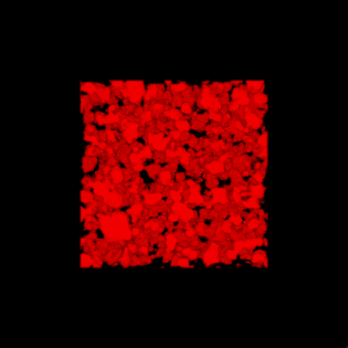
3-D rendering of the nanoparticle bijel taken by confocal microscope. (Credit: Caili Huang/ORNL [Oak Ridge National Laboratory] and Joe Forth/Berkeley Lab)

Here’s a link to and a citation for the paper,

Bicontinuous structured liquids with sub-micrometre domains using nanoparticle surfactants by Caili Huang, Joe Forth, Weiyu Wang, Kunlun Hong, Gregory S. Smith, Brett A. Helms & Thomas P. Russell. Nature Nanotechnology (2017) doi:10.1038/nnano.2017.182 25 September 2017

This paper is behind a paywall.

Smart windows from Texas (US)

I’ve been waiting for ‘smart’ windows and/or self-cleaning windows since 2008. While this research on ‘smart’ windows at the University of Texas at Austin looks promising I suspect it will be years before these things are in the marketplace. A July 22, 2015 news item on Nanotechnology Now announces the latest research,

Researchers in the Cockrell School of Engineering at The University of Texas at Austin are one step closer to delivering smart windows with a new level of energy efficiency, engineering materials that allow windows to reveal light without transferring heat and, conversely, to block light while allowing heat transmission, as described in two new research papers.

By allowing indoor occupants to more precisely control the energy and sunlight passing through a window, the new materials could significantly reduce costs for heating and cooling buildings.

In 2013, chemical engineering professor Delia Milliron and her team became the first to develop dual-band electrochromic materials that blend two materials with distinct optical properties for selective control of visible and heat-producing near-infrared light (NIR). In a 2013 issue of Nature, Milliron’s research group demonstrated how, using a small jolt of electricity, a nanocrystal material could be switched back and forth, enabling independent control of light and energy.

A July 23, 2015 University of Texas at Austin news release, which originated the news item, provides more details about the research which has spawned two recently published papers,

The team now has engineered two new advancements in electrochromic materials — a highly selective cool mode and a warm mode — not thought possible several years ago.

The cool mode material is a major step toward a commercialized product because it enables control of 90 percent of NIR and 80 percent of the visible light from the sun and takes only minutes to switch between modes. The previously reported material could require hours.

To achieve this high performance, Milliron and a team, including Cockrell School postdoctoral researcher Jongwook Kim and collaborator Brett Helms of the Lawrence Berkeley National Lab, developed a new nanostructured architecture for electrochromic materials that allows for a cool mode to block near-infrared light while allowing the visible light to shine through. This could help reduce energy costs for cooling buildings and homes during the summer. The researchers reported the new architecture in Nano Letters on July 20.

“We believe our new architected nanocomposite could be seen as a model material, establishing the ideal design for a dual-band electrochromic material,” Milliron said. “This material could be ideal for application as a smart electrochromic window for buildings.”

In the paper, the team demonstrates how the new material can strongly and selectively modulate visible light and NIR by applying a small voltage.

To optimize the performance of electrochromics for practical use, the team organized the two components of the composite material to create a porous interpenetrating network. The framework architecture provides channels for transport of electronic and ionic change. This organization enables substantially faster switching between modes.
Smart Window

The researchers are now working to produce a similarly structured nanocomposite material by simple methods, suitable for low-cost manufacturing.

In a second research paper, Milliron and her team, including Cockrell School graduate student Clayton Dahlman, have reported a proof-of-concept demonstrating how they can achieve optical control properties in windows from a well-crafted, single-component film. The concept includes a simple coating that creates a new warm mode, in which visible light can be blocked, while near-infrared light can enter. This new setting could be most useful on a sunny winter day, when an occupant would want infrared radiation to pass into a building for warmth, but the glare from sunlight to be reduced.

In this paper, published in the Journal of the American Chemical Society, Milliron proved that a coating containing a single component ­— doped titania nanocrystals — could demonstrate dynamic control over the transmittance of solar radiation. Because of two distinct charging mechanisms found at different applied voltages, this material can selectively block visible or infrared radiation.

“These two advancements show that sophisticated dynamic control of sunlight is possible,” Milliron said. “We believe our deliberately crafted nanocrystal-based materials could meet the performance and cost targets needed to progress toward commercialization of smart windows.”

Interestingly, the news release includes this statement,

The University of Texas at Austin is committed to transparency and disclosure of all potential conflicts of interest. The lead UT investigator involved with this project, Delia Milliron, is the chief scientific officer and owns an equity position in Heliotrope Technologies, an early-stage company developing new materials and manufacturing processes for electrochromic devices with an emphasis on energy-saving smart windows. Milliron is associated with patents at Lawrence Berkeley National Laboratory licensed to Heliotrope Technologies. Collaborator Brett Helms serves on the scientific advisory board of Heliotrope and owns equity in the company.

Here are links to and citations for the two papers,

Nanocomposite Architecture for Rapid, Spectrally-Selective Electrochromic Modulation of Solar Transmittance by Jongwook Kim, Gary K. Ong, Yang Wang, Gabriel LeBlanc, Teresa E. Williams, Tracy M. Mattox, Brett A. Helms, and Delia J. Milliron. Nano Lett., Article ASAP DOI: 10.1021/acs.nanolett.5b02197 Publication Date (Web): July 20, 2015

Copyright © 2015 American Chemical Society

Spectroelectrochemical Signatures of Capacitive Charging and Ion Insertion in Doped Anatase Titania Nanocrystals by Clayton J. Dahlman, Yizheng Tan, Matthew A. Marcus, and Delia J. Milliron. J. Am. Chem. Soc., 2015, 137 (28), pp 9160–9166 DOI: 10.1021/jacs.5b04933 Publication Date (Web): July 8, 2015

Copyright © 2015 American Chemical Society

These papers are behind paywalls.

Cooling it—an application using carbon nanotubes and a theory that hotter leads to cooler

The only thing these two news items have in common is their focus on cooling down electronic devices. Well, there’s also the fact that the work is being done at the nanoscale.

First, there’s a Jan. 23, 2014 news item on Azonano about a technique using carbon nanotubes to cool down microprocessors,

“Cool it!” That’s a prime directive for microprocessor chips and a promising new solution to meeting this imperative is in the offing. Researchers with the U.S. Department of Energy (DOE)’s Lawrence Berkeley National Laboratory (Berkeley Lab) have developed a “process friendly” technique that would enable the cooling of microprocessor chips through carbon nanotubes.

Frank Ogletree, a physicist with Berkeley Lab’s Materials Sciences Division, led a study in which organic molecules were used to form strong covalent bonds between carbon nanotubes and metal surfaces. This improved by six-fold the flow of heat from the metal to the carbon nanotubes, paving the way for faster, more efficient cooling of computer chips. The technique is done through gas vapor or liquid chemistry at low temperatures, making it suitable for the manufacturing of computer chips.

The Jan. 22, 2014 Berkeley Lab news release (also on EurekAlert), which originated the news item, describes the nature  of the problem in more detail,

Overheating is the bane of microprocessors. As transistors heat up, their performance can deteriorate to the point where they no longer function as transistors. With microprocessor chips becoming more densely packed and processing speeds continuing to increase, the overheating problem looms ever larger. The first challenge is to conduct heat out of the chip and onto the circuit board where fans and other techniques can be used for cooling. Carbon nanotubes have demonstrated exceptionally high thermal conductivity but their use for cooling microprocessor chips and other devices has been hampered by high thermal interface resistances in nanostructured systems.

“The thermal conductivity of carbon nanotubes exceeds that of diamond or any other natural material but because carbon nanotubes are so chemically stable, their chemical interactions with most other materials are relatively weak, which makes for  high thermal interface resistance,” Ogletree says. “Intel came to the Molecular Foundry wanting to improve the performance of carbon nanotubes in devices. Working with Nachiket Raravikar and Ravi Prasher, who were both Intel engineers when the project was initiated, we were able to increase and strengthen the contact between carbon nanotubes and the surfaces of other materials. This reduces thermal resistance and substantially improves heat transport efficiency.”

The news release then describes the proposed solution,

Sumanjeet Kaur, lead author of the Nature Communications paper and an expert on carbon nanotubes, with assistance from co-author and Molecular Foundry chemist Brett Helms, used reactive molecules to bridge the carbon nanotube/metal interface – aminopropyl-trialkoxy-silane (APS) for oxide-forming metals, and cysteamine for noble metals. First vertically aligned carbon nanotube arrays were grown on silicon wafers, and thin films of aluminum or gold were evaporated on glass microscope cover slips. The metal films were then “functionalized” and allowed to bond with the carbon nanotube arrays. Enhanced heat flow was confirmed using a characterization technique developed by Ogletree that allows for interface-specific measurements of heat transport.

“You can think of interface resistance in steady-state heat flow as being an extra amount of distance the heat has to flow through the material,” Kaur says. “With carbon nanotubes, thermal interface resistance adds something like 40 microns of distance on each side of the actual carbon nanotube layer. With our technique, we’re able to decrease the interface resistance so that the extra distance is around seven microns at each interface.”

Although the approach used by Ogletree, Kaur and their colleagues substantially strengthened the contact between a metal and individual carbon nanotubes within an array, a majority of the nanotubes within the array may still fail to connect with the metal. The Berkeley team is now developing a way to improve the density of carbon nanotube/metal contacts. Their technique should also be applicable to single and multi-layer graphene devices, which face the same cooling issues.

For anyone who’s never heard of the Molecular Foundry before (from the news release),

The Molecular Foundry is one of five DOE [Department of Energy] Nanoscale Science Research Centers (NSRCs), national user facilities for interdisciplinary research at the nanoscale, supported by the DOE Office of Science. Together the NSRCs comprise a suite of complementary facilities that provide researchers with state-of-the-art capabilities to fabricate, process, characterize, and model nanoscale materials, and constitute the largest infrastructure investment of the National Nanotechnology Initiative. The NSRCs are located at DOE’s Argonne, Brookhaven, Lawrence Berkeley, Oak Ridge and Sandia and Los Alamos national laboratories.

My second item comes from the University of Buffalo (UB), located in the US. From a Jan. 21, 2014 University of Buffalo news release by Cory Nealon (also on EurekAlert),

Heat in electronic devices is generated by the movement of electrons through transistors, resistors and other elements of an electrical network. Depending on the network, there are a variety of ways, such as cooling fans and heat sinks, to prevent the circuits from overheating.

But as more integrated circuits and transistors are added to devices to boost their computing power, it’s becoming more difficult to keep those elements cool. Most nanoelectrics research centers are working to develop advanced materials that are capable of withstanding the extreme environment inside smartphones, laptops and other devices.

While advanced materials show tremendous potential, the UB research suggests there may still be room within the existing paradigm of electronic devices to continue developing more powerful computers.

To support their findings, the researchers fabricated nanoscale semiconductor devices in a state-of-the-art gallium arsenide crystal provided to UB by Sandia’s Reno [John L. Reno, Center for Integrated Nanotechnologies at Sandia National Laboratories]. The researchers then subjected the chip to a large voltage, squeezing an electrical current through the nanoconductors. This, in turn, increased the amount of heat circulating through the chip’s nanotransistor.

But instead of degrading the device, the nanotransistor spontaneously transformed itself into a quantum state that was protected from the effect of heating and provided a robust channel of electric current. To help explain, Bird [Jonathan Bird, UB professor of electrical engineering] offered an analogy to Niagara Falls.

“The water, or energy, comes from a source; in this case, the Great Lakes. It’s channeled into a narrow point (the Niagara River) and ultimately flows over Niagara Falls. At the bottom of waterfall is dissipated energy. But unlike the waterfall, this dissipated energy recirculates throughout the chip and changes how heat affects, or in this case doesn’t affect, the network’s operation.”

While this behavior may seem unusual, especially conceptualizing it in terms of water flowing over a waterfall, it is the direct result of the quantum mechanical nature of electronics when viewed on the nanoscale. The current is made up of electrons which spontaneously organize to form a narrow conducting filament through the nanoconductor. It is this filament that is so robust against the effects of heating.

“We’re not actually eliminating the heat, but we’ve managed to stop it from affecting the electrical network. In a way, this is an optimization of the current paradigm,” said Han [J. E. Han, UB Dept. of Physics], who developed the theoretical models which explain the findings.

What an interesting and counter-intuitive approach to managing the heat in our devices.

For those who want more, here’s a link to and citation for the carbon nanotube paper,

Enhanced thermal transport at covalently functionalized carbon nanotube array interfaces by Sumanjeet Kaur, Nachiket Raravikar, Brett A. Helms, Ravi Prasher, & D. Frank Ogletree. Nature Communications 5, Article number: 3082 doi:10.1038/ncomms4082 Published 22 January 2014

This paper is behind a paywall.

Now here’s a link to and a citation for the ‘making it hotter to make it cooler’ paper,

Formation of a protected sub-band for conduction in quantum point contacts under extreme biasing by J. Lee, J. E. Han, S. Xiao, J. Song, J. L. Reno, & J. P. Bird. Nature Nanotechnology (2014) doi:10.1038/nnano.2013.297 Published online 19 January 2014

This paper is behind a paywall although there is an option to preview it for free via ReadCube Access.