This is a different approach to neuromorphic (brainlike) computing being described in an August 28, 2023 news item on phys.org, Note: A link has been removed,
The word “fractals” might inspire images of psychedelic colors spiraling into infinity in a computer animation. An invisible, but powerful and useful, version of this phenomenon exists in the realm of dynamic magnetic fractal networks.
Dustin Gilbert, assistant professor in the Department of Materials Science and Engineering [University of Tennessee, US], and colleagues have published new findings in the behavior of these networks—observations that could advance neuromorphic computing capabilities.
Their research is detailed in their article “Skyrmion-Excited Spin-Wave Fractal Networks,” cover story for the August 17, 2023, issue of Advanced Materials.
“Most magnetic materials—like in refrigerator magnets—are just comprised of domains where the magnetic spins all orient parallel,” said Gilbert. “Almost 15 years ago, a German research group discovered these special magnets where the spins make loops—like a nanoscale magnetic lasso. These are called skyrmions.”
Named for legendary particle physicist Tony Skyrme, a skyrmion’s magnetic swirl gives it a non-trivial topology. As a result of this topology, the skyrmion has particle-like properties—they are hard to create or destroy, they can move and even bounce off of each other. The skyrmion also has dynamic modes—they can wiggle, shake, stretch, whirl, and breath[e].
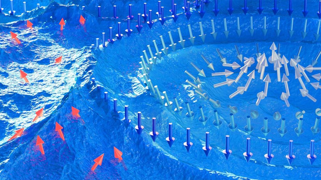
As the skyrmions “jump and jive,” they are creating magnetic spin waves with a very narrow wavelength. The interactions of these waves form an unexpected fractal structure.
“Just like a person dancing in a pool of water, they generate waves which ripple outward,” said Gilbert. “Many people dancing make many waves, which normally would seem like a turbulent, chaotic sea. We measured these waves and showed that they have a well-defined structure and collectively form a fractal which changes trillions of times per second.”
Fractals are important and interesting because they are inherently tied to a “chaos effect”—small changes in initial conditions lead to big changes in the fractal network.
“Where we want to go with this is that if you have a skyrmion lattice and you illuminate it with spin waves, the way the waves make its way through this fractal-generating structure is going to depend very intimately on its construction,” said Gilbert. “So, if you could write individual skyrmions, it can effectively process incoming spin waves into something on the backside—and it’s programmable. It’s a neuromorphic architecture.”
The Advanced Materials cover illustration [image at top of this posting] depicts a visual representation of this process, with the skyrmions floating on top of a turbulent blue sea illustrative of the chaotic structure generated by the spin wave fractal.
“Those waves interfere just like if you throw a handful of pebbles into a pond,” said Gilbert. “You get a choppy, turbulent mess. But it’s not just any simple mess, it’s actually a fractal. We have an experiment now showing that the spin waves generated by skyrmions aren’t just a mess of waves, they have inherent structure of their very own. By, essentially, controlling those stones that we ‘throw in,’ you get very different patterns, and that’s what we’re driving towards.”
The discovery was made in part by neutron scattering experiments at the Oak Ridge National Laboratory (ORNL) High Flux Isotope Reactor and at the National Institute of Standards and Technology (NIST) Center for Neutron Research. Neutrons are magnetic and pass through materials easily, making them ideal probes for studying materials with complex magnetic behavior such as skyrmions and other quantum phenomena.
Gilbert’s co-authors for the new article are Nan Tang, Namila Liyanage, and Liz Quigley, students in his research group; Alex Grutter and Julie Borchers from National Institute of Standards and Technology (NIST), Lisa DeBeer-Schmidt and Mike Fitzsimmons from Oak Ridge National Laboratory; and Eric Fullerton, Sheena Patel, and Sergio Montoya from the University of California, San Diego.
The team’s next step is to build a working model using the skyrmion behavior.
“If we can develop thinking computers, that, of course, is extraordinarily important,” said Gilbert. “So, we will propose to make a miniaturized, spin wave neuromorphic architecture.” He also hopes that the ripples from this UT Knoxville discovery inspire researchers to explore uses for a spiraling range of future applications.
Here’s a link to and a citation for the paper,
Skyrmion-Excited Spin-Wave Fractal Networks by Nan Tang, W. L. N. C. Liyanage, Sergio A. Montoya, Sheena Patel, Lizabeth J. Quigley, Alexander J. Grutter, Michael R. Fitzsimmons, Sunil Sinha, Julie A. Borchers, Eric E. Fullerton, Lisa DeBeer-Schmitt, Dustin A. Gilbert. Advanced Materials Volume 35, Issue 33 August 17, 2023 2300416 DOI: https://doi.org/10.1002/adma.202300416 First published: 04 May 2023
Nice to learn of this news, which is on the CBC (Canadian Broadcasting Corporation) news online website. From a December 13, 2022 news item provided by Associated Press (Note: the news item was updated to include general description and some Canadian content at about 12 pm PT) ,
…
Researchers at the Lawrence Livermore National Laboratory in California for the first time produced more energy in a fusion reaction than was used to ignite it, [emphasis mine] something called net energy gain, the Energy Department said.
…
Peter Behr’s December 13, 2022 article on Politico.com about the US Department of Energy’s big announcement also breaks the news,
The Department of Energy announced Tuesday [December 12, 2022] that its scientists have produced the first ever fusion reaction that yielded more energy than the reaction required, an essential step in the long path toward commercial fusion power, officials said.
The experiment Dec. 5 [2022], at the Lawrence Livermore National Laboratory in California, took a few billionths of second. But laboratory leaders said today that it demonstrated for the first time that sustained fusion power is possible.
…
Behr explains what nuclear fusion is but first he touches on why scientists are so interested in the process, from his December 13, 2022 article,
…
In theory, nuclear fusion could produce massive amounts of energy without producing lost-lasting radioactive waste, or posing the risk of meltdowns. That’s unlike nuclear fission, which powers today’s reactors.
Fission results when radioactive atoms — most commonly uranium — are split by neutrons in controlled chain reactions, creating lighter atoms and large amounts of radiation and energy to produce electric power.
Fusion is the opposite process. In the most common approach, swirling hydrogen isotopes are forced together under tremendous heat to create helium and energy for power generation. This is the same process that powers the sun and other stars. But scientists have been trying since the mid-20th century to find a way to use it to generate power on Earth.
…
There are two main approaches to making fusion happen and I found a description for them in an October 2022 article about local company, General Fusion, by Nelson Bennett for Business in Vancouver magazine (paper version),
Most fusion companies are pursuing one of two approaches: Magnet [sic] or inertial confinement. General fusion is one of the few that is taking a more hybrid approach ¬ magnetic confinement with pulse compression.
Fusion occurs when smaller nuclei are fused together under tremendous force into larger nuclei, with a release of energy occurring in the form of neutrons. It’s what happens to stars when gravitational force creates extreme heat that turns on the fusion engine.
Replicating that in a machine requires some form of confinement to squeeze plasma ¬ a kind of super-hot fog of unbound positive and negative particles ¬ to the point where nuclei fuse.
One approach is inertial confinement, in which lasers are focused on a small capsule of heavy hydrogen fuel (deuterium and tritium) to create ignition. This takes a tremendous amount of energy, and the challenge for all fusion efforts is to get a sustained ignition that produces more energy than it takes to get ignition ¬ called net energy gain.
The other main approach is magnetic confinement, using powerful magnets in a machine called a tokomak to contain and squeeze plasma into a donut-shaped form called a torus.
General Fusion uses magnets to confine the plasma, but to get ignition it uses pistons arrayed around a spherical chamber to fire synchronously to essentially collapse the plasma on itself and spark ignition.
General Fusion’s machine uses liquid metal spinning inside a chamber that acts as a protective barrier between the hot plasma and the machine ¬ basically a sphere of plasma contained within a sphere of liquid metal. This protects the machine from damage.
The temperatures generated in fusion ¬ up to to 150 million degrees Celsius ¬ are five to six times hotter than the core of the sun, and can destroy machines that produce them. This makes durability a big challenge in any machine.
…
The Lawrence Livermore National Laboratory (LLNL) issued a December 13, 2022 news release, which provides more detail about their pioneering work, Note: I have changed the order of the paragraphs but all of this is from the news release,
…
Fusion is the process by which two light nuclei combine to form a single heavier nucleus, releasing a large amount of energy. In the 1960s, a group of pioneering scientists at LLNL hypothesized that lasers could be used to induce fusion in a laboratory setting. Led by physicist John Nuckolls, who later served as LLNL director from 1988 to 1994, this revolutionary idea became inertial confinement fusion, kicking off more than 60 years of research and development in lasers, optics, diagnostics, target fabrication, computer modeling and simulation and experimental design.
To pursue this concept, LLNL built a series of increasingly powerful laser systems, leading to the creation of NIF [National Ignition Facility], the world’s largest and most energetic laser system. NIF — located at LLNL in Livermore, California — is the size of a sports stadium and uses powerful laser beams to create temperatures and pressures like those in the cores of stars and giant planets, and inside exploding nuclear weapons.
…
LLNL’s experiment surpassed the fusion threshold by delivering 2.05 megajoules (MJ) of energy to the target, resulting in 3.15 MJ of fusion energy output, demonstrating for the first time a most fundamental science basis for inertial fusion energy (IFE). Many advanced science and technology developments are still needed to achieve simple, affordable IFE to power homes and businesses, and DOE is currently restarting a broad-based, coordinated IFE program in the United States. Combined with private-sector investment, there is a lot of momentum to drive rapid progress toward fusion commercialization.
If you want to see some really excited comments from scientists just read the LLNL’s December 13, 2022 news release. Even the news release’s banner is exuberant,
Fearful that China might wind up dominating fusion energy in the second half of this century, Congress in 2020 told DOE [Department of Energy] to begin funding development of a utility-scale fusion pilot plant that could deliver at least 50 megawatts of power to the U.S. grid.
…
In September [2022], DOE invited private companies to apply for an initial $50 million in research grants to help fund development of detailed pilot plant plans.
“We’re seeking strong partnerships between DOE and the private sector,” a senior DOE official told POLITICO’s E&E News recently. The official was not willing to speak on the record, saying the grant process is ongoing and confidential.
As the competition proceeds, DOE will set technical milestones or requirements, challenging the teams to show how critical engineering challenges will be overcome. DOE’s goal is “hopefully to enable a fusion pilot to operate in the early 2030s,” the official added.
At least 15 U.S. and foreign fusion companies have submitted requests for an initial total of $50 million in pilot plant grants, and some of them are pursuing the laser-ignition fusion process that Lawrence Livermore has pioneered, said Holland. He did not name the companies because the competition is confidential.
…
I wonder if General Fusion whose CEO (Chief Executive Officer) Greg Twinney declared, “Commercializing fusion energy is within reach, and General Fusion is ready to deliver it to the grid by the 2030s …” (in a December 12, 2022 company press release) is part of the US competition.
I noticed that General Fusion lists this at the end of the press release,
… Founded in 2002, we are headquartered in Vancouver, Canada, with additional centers co-located with internationally recognized fusion research laboratories near London, U.K., and Oak Ridge, Tennessee, U.S.A.
The Oak Ridge National Laboratory (ORNL), like the LLNL, is a US Department of Energy research facility.
As for General Fusion’s London connection, I have more about that in my October 28, 2022 posting “Overview of fusion energy scene,” which includes General Fusion’s then latest news about a commercialization agreement with the UKAEA (UK Atomic Energy Authority) and a ‘fusion’ video by rapper Baba Brinkman along with the overview.
In early October 2022, Alain Aspect, John Clauser and Anton Zeilinger were jointly awarded the 2022 Nobel Prize in Physics for work each scientist performed independently of the others.
Alain Aspect Institut d’Optique Graduate School – Université Paris- Saclay and École Polytechnique, Palaiseau, France
John F. Clauser J.F. Clauser & Assoc., Walnut Creek, CA, USA
Anton Zeilinger University of Vienna, Austria
“for experiments with entangled photons, establishing the violation of Bell inequalities and pioneering quantum information science”
Entangled states – from theory to technology
Alain Aspect, John Clauser and Anton Zeilinger have each conducted groundbreaking experiments using entangled quantum states, where two particles behave like a single unit even when they are separated. Their results have cleared the way for new technology based upon quantum information.
The ineffable effects of quantum mechanics are starting to find applications. There is now a large field of research that includes quantum computers, quantum networks and secure quantum encrypted communication.
One key factor in this development is how quantum mechanics allows two or more particles to exist in what is called an entangled state. What happens to one of the particles in an entangled pair determines what happens to the other particle, even if they are far apart.
For a long time, the question was whether the correlation was because the particles in an entangled pair contained hidden variables, instructions that tell them which result they should give in an experiment. In the 1960s, John Stewart Bell developed the mathematical inequality that is named after him. This states that if there are hidden variables, the correlation between the results of a large number of measurements will never exceed a certain value. However, quantum mechanics predicts that a certain type of experiment will violate Bell’s inequality, thus resulting in a stronger correlation than would otherwise be possible.
John Clauser developed John Bell’s ideas, leading to a practical experiment. When he took the measurements, they supported quantum mechanics by clearly violating a Bell inequality. This means that quantum mechanics cannot be replaced by a theory that uses hidden variables.
Some loopholes remained after John Clauser’s experiment. Alain Aspect developed the setup, using it in a way that closed an important loophole. He was able to switch the measurement settings after an entangled pair had left its source, so the setting that existed when they were emitted could not affect the result.
Using refined tools and long series of experiments, Anton Zeilinger started to use entangled quantum states. Among other things, his research group has demonstrated a phenomenon called quantum teleportation, which makes it possible to move a quantum state from one particle to one at a distance.
“It has become increasingly clear that a new kind of quantum technology is emerging. We can see that the laureates’ work with entangled states is of great importance, even beyond the fundamental questions about the interpretation of quantum mechanics,”says Anders Irbäck, Chair of the Nobel Committee for Physics.
There are some practical applications for their work on establishing quantum entanglement as Dr. Nicholas Peters, University of Tennessee and Oak Ridge National Laboratory (ORNL), explains in his October 7, 2022 essay for The Conversation,
Unhackable communications devices, high-precision GPS and high-resolution medical imaging all have something in common. These technologies—some under development and some already on the market all rely on the non-intuitive quantum phenomenon of entanglement.
Two quantum particles, like pairs of atoms or photons, can become entangled. That means a property of one particle is linked to a property of the other, and a change to one particle instantly affects the other particle, regardless of how far apart they are. This correlation is a key resource in quantum information technologies.
For the most part, quantum entanglement is still a subject of physics research, but it’s also a component of commercially available technologies, and it plays a starring role in the emerging quantum information processing industry.
…
Quantum entanglement is a critical element of quantum information processing, and photonic entanglement of the type pioneered by the Nobel laureates is crucial for transmitting quantum information. Quantum entanglement can be used to build large-scale quantum communications networks.
On a path toward long-distance quantum networks, Jian-Wei Pan, one of Zeilinger’s former students, and colleagues demonstrated entanglement distribution to two locations separated by 764 miles (1,203 km) on Earth via satellite transmission. However, direct transmission rates of quantum information are limited due to loss, meaning too many photons get absorbed by matter in transit so not enough reach the destination.
Entanglement is critical for solving this roadblock, through the nascent technology of quantum repeaters. An important milestone for early quantum repeaters, called entanglement swapping, was demonstrated by Zeilinger and colleagues in 1998. Entanglement swapping links one each of two pairs of entangled photons, thereby entangling the two initially independent photons, which can be far apart from each other.
…
Perhaps the most well known quantum communications application is Quantum Key Distribution (QKD), which allows someone to securely distribute encryption keys. If those keys are stored properly, they will be secure, even from future powerful, code-breaking quantum computers.
…
I don’t usually embed videos that are longer than 5 mins. but this one has a good explanation of cryptography (both classical and quantum),
The video host, Physics Girl (website), is also known as Dianna Cowern.
I wonder if there’s going to be a rush to fund and commercialize more quantum physics projects. There’s certainly an upsurge in activity locally and in Canada (I assume the same is true elsewhere) as my July 26, 2022 posting “Quantum Mechanics & Gravity conference (August 15 – 19, 2022) launches Vancouver (Canada)-based Quantum Gravity Institute and more” makes clear.
At the simplest of levels, nanopores are (nanometre-sized) holes in an insulating membrane. The hole allows ions to pass through the membrane when a voltage is applied, resulting in a measurable current. When a molecule passes through a nanopore it causes a change in the current, this can be used to characterize and even identify individual molecules. Nanopores are extremely powerful single-molecule biosensing devices and can be used to detect and sequence DNA, RNA, and even proteins. Recently, it has been used in the SARS-CoV-2 virus sequencing.
Solid-state nanopores are an extremely versatile type of nanopore formed in ultrathin membranes (less than 50 nanometres), made from materials such as silicon nitride (SiNx). Solid-state nanopores can be created with a range of diameters and can withstand a multitude of conditions (discover more about solid-state nanopore fabrication techniques here). One of the most appealing techniques with which to fabricate nanopores is Controlled Breakdown (CBD). This technique is quick, reduces fabrication costs, does not require specialized equipment, and can be automated.
CBD is a technique in which an electric field is applied across the membrane to induce a current. At some point, a spike in the current is observed, signifying pore formation. The voltage is then quickly reduced to ensure the fabrication of a single, small nanopore.
The mechanisms underlying this process have not been fully elucidated thus an international team involving ITQB NOVA decided to further investigate how electrical conduction through the membrane occurs during breakdown, namely how oxidation and reduction reactions (also called redox reactions, they imply electron loss or gain, respectively) influence the process. To do this, the team created three devices in which the electric field is applied to the membrane (a silicon-rich SiNx membrane) in different ways: via metal electrodes on both sides of the membrane; via electrolyte solutions on both sides of the membrane; and via a mixed device with a metal electrode on one side and an electrolyte solution on the other.
Results showed that redox reactions must occur at the membrane-electrolyte interface, whilst the metal electrodes circumvent this need. The team also demonstrated that, because of this phenomenon, nanopore fabrication could be localized to certain regions by performing CBD with metal microelectrodes on the membrane surface. Finally, by varying the content of silicon in the membrane, the investigators demonstrated that conduction and nanopore formation is highly dependent on the membrane material since it limits the electrical current in the membrane.
“Controlling the location of nanopores has been of interest to us for a number of years”, says James Yates. Pedro Sousa adds that “our findings suggest that CBD can be used to integrate pores with complementary micro or nanostructures, such as tunneling electrodes or field-effect sensors, across a range of different membrane materials.” These devices may then be used for the detection of specific molecules, such as proteins, DNA, or antibodies, and applied to a wide array of scenarios, including pandemic surveillance or food safety.
This project was developed by a research team led by ITQB NOVA’s James Yates and has received funding from the European Research Council (ERC) under the European Union’s Horizon 2020 research and innovation program (grant agreement No 724300 and 875525). Co-author Pedro Miguel Sousa is also from ITQB NOVA. The other consortium members are from the University of Oxford, Oak Ridge National Laboratory, Imperial College London and Queen Mary University of London. The authors would like to thank Andrew Briggs for providing financial support.
Here’s a link to and a citation for the paper,
Understanding Electrical Conduction and Nanopore Formation During Controlled Breakdown by Jasper P. Fried, Jacob L. Swett, Binoy Paulose Nadappuram, Aleksandra Fedosyuk, Pedro Miguel Sousa, Dayrl P. Briggs, Aleksandar P. Ivanov, Joshua B. Edel, Jan A. Mol, James R. Yates. Small DOI: https://doi.org/10.1002/smll.202102543 First published: 01 August 2021
Caption: Researchers at ORNL’s Center for Nanophase Materials Sciences demonstrated the first example of capacitance in a lipid-based biomimetic membrane, opening nondigital routes to advanced, brain-like computation. Credit: Michelle Lehman/Oak Ridge National Laboratory, U.S. Dept. of Energy
The last time I wrote about memcapacitors (June 30, 2014 posting: Memristors, memcapacitors, and meminductors for faster computers), the ideas were largely theoretical; I believe this work is the first research I’ve seen on the topic. From an October 17, 2019 news item on ScienceDaily,
Researchers at the Department of Energy’s Oak Ridge National Laboratory ]ORNL], the University of Tennessee and Texas A&M University demonstrated bio-inspired devices that accelerate routes to neuromorphic, or brain-like, computing.
Results published in Nature Communications report the first example of a lipid-based “memcapacitor,” a charge storage component with memory that processes information much like synapses do in the brain. Their discovery could support the emergence of computing networks modeled on biology for a sensory approach to machine learning.
“Our goal is to develop materials and computing elements that work like biological synapses and neurons—with vast interconnectivity and flexibility—to enable autonomous systems that operate differently than current computing devices and offer new functionality and learning capabilities,” said Joseph Najem, a recent postdoctoral researcher at ORNL’s Center for Nanophase Materials Sciences, a DOE Office of Science User Facility, and current assistant professor of mechanical engineering at Penn State.
The novel approach uses soft materials to mimic biomembranes and simulate the way nerve cells communicate with one another.
The team designed an artificial cell membrane, formed at the interface of two lipid-coated water droplets in oil, to explore the material’s dynamic, electrophysiological properties. At applied voltages, charges build up on both sides of the membrane as stored energy, analogous to the way capacitors work in traditional electric circuits.
But unlike regular capacitors, the memcapacitor can “remember” a previously applied voltage and—literally—shape how information is processed. The synthetic membranes change surface area and thickness depending on electrical activity. These shapeshifting membranes could be tuned as adaptive filters for specific biophysical and biochemical signals.
“The novel functionality opens avenues for nondigital signal processing and machine learning modeled on nature,” said ORNL’s Pat Collier, a CNMS staff research scientist.
A distinct feature of all digital computers is the separation of processing and memory. Information is transferred back and forth from the hard drive and the central processor, creating an inherent bottleneck in the architecture no matter how small or fast the hardware can be.
Neuromorphic computing, modeled on the nervous system, employs architectures that are fundamentally different in that memory and signal processing are co-located in memory elements—memristors, memcapacitors and meminductors.
These “memelements” make up the synaptic hardware of systems that mimic natural information processing, learning and memory.
Systems designed with memelements offer advantages in scalability and low power consumption, but the real goal is to carve out an alternative path to artificial intelligence, said Collier.
Tapping into biology could enable new computing possibilities, especially in the area of “edge computing,” such as wearable and embedded technologies that are not connected to a cloud but instead make on-the-fly decisions based on sensory input and past experience.
Biological sensing has evolved over billions of years into a highly sensitive system with receptors in cell membranes that are able to pick out a single molecule of a specific odor or taste. “This is not something we can match digitally,” Collier said.
Digital computation is built around digital information, the binary language of ones and zeros coursing through electronic circuits. It can emulate the human brain, but its solid-state components do not compute sensory data the way a brain does.
“The brain computes sensory information pushed through synapses in a neural network that is reconfigurable and shaped by learning,” said Collier. “Incorporating biology—using biomembranes that sense bioelectrochemical information—is key to developing the functionality of neuromorphic computing.”
While numerous solid-state versions of memelements have been demonstrated, the team’s biomimetic elements represent new opportunities for potential “spiking” neural networks that can compute natural data in natural ways.
Spiking neural networks are intended to simulate the way neurons spike with electrical potential and, if the signal is strong enough, pass it on to their neighbors through synapses, carving out learning pathways that are pruned over time for efficiency.
A bio-inspired version with analog data processing is a distant aim. Current early-stage research focuses on developing the components of bio-circuitry.
“We started with the basics, a memristor that can weigh information via conductance to determine if a spike is strong enough to be broadcast through a network of synapses connecting neurons,” said Collier. “Our memcapacitor goes further in that it can actually store energy as an electric charge in the membrane, enabling the complex ‘integrate and fire’ activity of neurons needed to achieve dense networks capable of brain-like computation.”
The team’s next steps are to explore new biomaterials and study simple networks to achieve more complex brain-like functionalities with memelements.
Here’s a link to and a citation for the paper,
Dynamical nonlinear memory capacitance in biomimetic membranes by Joseph S. Najem, Md Sakib Hasan, R. Stanley Williams, Ryan J. Weiss, Garrett S. Rose, Graham J. Taylor, Stephen A. Sarles & C. Patrick Collier. Nature Communications volume 10, Article number: 3239 (2019) DOI: DOIhttps://doi.org/10.1038/s41467-019-11223-8 Published July 19, 2019
This paper is open access.
One final comment, you might recognize one of the authors (R. Stanley Williams) who in 2008 helped launch ‘memristor’ research.
While it’s true enough in English where you don’t spell the word team with the letter ‘I’, that’s not the case in French where the word is ‘equipe’. it makes me wonder how many other languages in the world have an ‘I’ in team.
Moving on. This English language saying is true enough in its way but there is no team unless you have a group of ‘I’s’ and the trick is getting them to work together as a July 18, 2019 Northwestern University news release (received via email) about a new online training tool notes,
Coaching scientists to play well together
Free tool shows how to avoid fights over data and authorship conflicts
‘You stole my idea’ or ‘I’m not getting credit for my work’ are common disputes Only tool validated by research to help scientists collaborate smoothly Many NSF [US National Science Foundation] and NIH [US National Institutes of Health] grants now require applicants to show readiness for team science Scientists can’t do it on their own
CHICAGO — When scientists from different disciplines collaborate – as is increasingly necessary to confront the complexity of challenging research problems – interpersonal tussles often arise. One scientist may accuse another of stealing her ideas. Or, a researcher may feel he is not getting credit for his work or doesn’t have access to important data.
“Interdisciplinary team science is now the state of the art across all branches of science and engineering,” said Bonnie Spring, professor of preventive medicine at Northwestern University Feinberg School of Medicine. “But very few scientists have been trained to work with others outside of their own disciplinary silo.”
The skill is critical because many National Institute[s] of Health and National Science Foundationgrants require applicants to show readiness for team science.
A free, online training tool developed by Northwestern — teamscience.net — has been been proven to help scientists develop skills to work with other scientists outside their own discipline.
A new study led by Spring showed scientists who completed the program’s modules – called COALESCE – significantly boosted their knowledge about team science and increased their self-confidence about being able to successfully work in scientific teams. Most people who completed one or more modules (84%) said that the experience of taking the modules was very likely to positively impact their future research.
The study will be published July 18 [2019] in the Journal of Clinical and Translational Science.
There are few training resources to teach scientists how to collaborate, and the ones that are available don’t have evidence of their effectiveness. Teamscience.net is the only free, validated-by-research tool available to anyone at any time.
Almost 1,000 of the COALESCE users opted voluntarily to respond to questions about the learning modules, providing information about how taking each module influenced team science knowledge, skills and attitudes.
‘You stole my idea’
The most common area of dispute among collaborating scientists is authorship concerns, such as accusations that one person stole ideas from another or that a contributor was not getting credit for his or her work, the study authors said. Other disputes arise around access to and analysis of data, utilization of materials or resources and the general direction of the research itself. Underlying all of these issues is a common failure to prepare for working collaboratively with other scientists.
“Preparing in advance before starting to collaborate, often through the creation of a formal collaboration agreement document, is the best way to head off these types of disputes,” said Angela Pfammatter, assistant professor of preventive medicine at Feinberg and a coauthor on the paper.
Spring suggested “having scientists discuss their expectations of one another and the collaboration to prevent acrimonious conflicts.”
Skills to play well together
These skills are critical to a successful scientific team, the authors said:
The ability to choose team members who have the right mix of expertise, temperament and accessibility to round out a team. The ability to anticipate what could go wrong and to develop contingency plans in advance. The ability to manage conflict within the team
The teamscience.net modules help scientists acquire these skills by letting them interact with different problem scenarios that can arise in team-based research. Scientists can try out different solutions and learn from mistakes in a safe, online environment.
More than 16,000 people have accessed the resource in the past six years. Demand for team science training is expected to increase as interdisciplinary teams set out to tackle some of science’s most challenging problems.
Other Northwestern authors on the paper are Ekaterina Klyachko, Phillip Rak, H. Gene McFadden, Juned Siddique and Leland Bardsley.
Funding support for COALESCE is from the National Institutes of Health, National Center for Advancing Translational Sciences grants 3UL1RR025741 and UL1TR001422 and its Office of Behavioral and Social Sciences Research.
i once got caught here on this blog between two warring scientists. My August 24, 2015 posting was a pretty standard one for me. Initially, it was one of my more minimalistic pieces with a copy of the text from a university news release announcing the research and a link to the academic paper. I can’t remember if the problem was which scientist was listed first and which was listed last but one of them took exception and contacted me explaining how it was wrong. (Note: These decisions are not made by me.) I did my best to fix whatever the problem was and then the other scientist contacted me. After the dust settled, I ended up with a dog’s breakfast for my posting and a new policy.
Getting back to COALESCE: I wish the Northwestern University researchers all the best as they look for ways to help scientists work together more smoothly and cooperatively.
I think this form of ‘cannibalism’ could also be described as a form of ‘self-assembly’. That said, here is an August 31, 2018 news item on ScienceDaily announcing ‘cannibalistic’ materials,
Scientists at the [US] Department of Energy’s [DOE] Oak Ridge National Laboratory [ORNL] induced a two-dimensional material to cannibalize itself for atomic “building blocks” from which stable structures formed.
The findings, reported in Nature Communications, provide insights that may improve design of 2D materials for fast-charging energy-storage and electronic devices.
“Under our experimental conditions, titanium and carbon atoms can spontaneously form an atomically thin layer of 2D transition-metal carbide, which was never observed before,” said Xiahan Sang of ORNL.
He and ORNL’s Raymond Unocic led a team that performed in situ experiments using state-of-the-art scanning transmission electron microscopy (STEM), combined with theory-based simulations, to reveal the mechanism’s atomistic details.
“This study is about determining the atomic-level mechanisms and kinetics that are responsible for forming new structures of a 2D transition-metal carbide such that new synthesis methods can be realized for this class of materials,” Unocic added.
The starting material was a 2D ceramic called a MXene (pronounced “max een”). Unlike most ceramics, MXenes are good electrical conductors because they are made from alternating atomic layers of carbon or nitrogen sandwiched within transition metals like titanium.
The research was a project of the Fluid Interface Reactions, Structures and Transport (FIRST) Center, a DOE Energy Frontier Research Center that explores fluid–solid interface reactions that have consequences for energy transport in everyday applications. Scientists conducted experiments to synthesize and characterize advanced materials and performed theory and simulation work to explain observed structural and functional properties of the materials. New knowledge from FIRST projects provides guideposts for future studies.
The high-quality material used in these experiments was synthesized by Drexel University scientists, in the form of five-ply single-crystal monolayer flakes of MXene. The flakes were taken from a parent crystal called “MAX,” which contains a transition metal denoted by “M”; an element such as aluminum or silicon, denoted by “A”; and either a carbon or nitrogen atom, denoted by “X.” The researchers used an acidic solution to etch out the monoatomic aluminum layers, exfoliate the material and delaminate it into individual monolayers of a titanium carbide MXene (Ti3C2).
The ORNL scientists suspended a large MXene flake on a heating chip with holes drilled in it so no support material, or substrate, interfered with the flake. Under vacuum, the suspended flake was exposed to heat and irradiated with an electron beam to clean the MXene surface and fully expose the layer of titanium atoms.
MXenes are typically inert because their surfaces are covered with protective functional groups—oxygen, hydrogen and fluorine atoms that remain after acid exfoliation. After protective groups are removed, the remaining material activates. Atomic-scale defects—“vacancies” created when titanium atoms are removed during etching—are exposed on the outer ply of the monolayer. “These atomic vacancies are good initiation sites,” Sang said. “It’s favorable for titanium and carbon atoms to move from defective sites to the surface.” In an area with a defect, a pore may form when atoms migrate.
“Once those functional groups are gone, now you’re left with a bare titanium layer (and underneath, alternating carbon, titanium, carbon, titanium) that’s free to reconstruct and form new structures on top of existing structures,” Sang said.
High-resolution STEM imaging proved that atoms moved from one part of the material to another to build structures. Because the material feeds on itself, the growth mechanism is cannibalistic.
“The growth mechanism is completely supported by density functional theory and reactive molecular dynamics simulations, thus opening up future possibilities to use these theory tools to determine the experimental parameters required for synthesizing specific defect structures,” said Adri van Duin of Penn State [Pennsylvania State University].
Most of the time, only one additional layer [of carbon and titanium] grew on a surface. The material changed as atoms built new layers. Ti3C2 turned into Ti4C3, for example.
“These materials are efficient at ionic transport, which lends itself well to battery and supercapacitor applications,” Unocic said. “How does ionic transport change when we add more layers to nanometer-thin MXene sheets?” This question may spur future studies.
“Because MXenes containing molybdenum, niobium, vanadium, tantalum, hafnium, chromium and other metals are available, there are opportunities to make a variety of new structures containing more than three or four metal atoms in cross-section (the current limit for MXenes produced from MAX phases),” Yury Gogotsi of Drexel University added. “Those materials may show different useful properties and create an array of 2D building blocks for advancing technology.”
At ORNL’s Center for Nanophase Materials Sciences (CNMS), Yu Xie, Weiwei Sun and Paul Kent performed first-principles theory calculations to explain why these materials grew layer by layer instead of forming alternate structures, such as squares. Xufan Li and Kai Xiao helped understand the growth mechanism, which minimizes surface energy to stabilize atomic configurations. Penn State scientists conducted large-scale dynamical reactive force field simulations showing how atoms rearranged on surfaces, confirming defect structures and their evolution as observed in experiments.
The researchers hope the new knowledge will help others grow advanced materials and generate useful nanoscale structures.
Here’s a link to and a citation for the paper,
In situ atomistic insight into the growth mechanisms of single layer 2D transition metal carbides by Xiahan Sang, Yu Xie, Dundar E. Yilmaz, Roghayyeh Lotfi, Mohamed Alhabeb, Alireza Ostadhossein, Babak Anasori, Weiwei Sun, Xufan Li, Kai Xiao, Paul R. C. Kent, Adri C. T. van Duin, Yury Gogotsi, & Raymond R. Unocic. Nature Communicationsvolume 9, Article number: 2266 (2018) DOI: https://doi.org/10.1038/s41467-018-04610-0 Published 11 June 2018
I’d have to see it to believe it but researchers at the US Dept. of Energy (DOE) Lawrence Berkeley National Laboratory (LBNL) have developed a new kind of ‘bijel’ which would allow for some pretty nifty robotics. From a Sept. 25, 2017 news item on ScienceDaily,
A new two-dimensional film, made of polymers and nanoparticles and developed by researchers at the Department of Energy’s Lawrence Berkeley National Laboratory (Berkeley Lab), can direct two different non-mixing liquids into a variety of exotic architectures. This finding could lead to soft robotics, liquid circuitry, shape-shifting fluids, and a host of new materials that use soft, rather than solid, substances.
The study, reported today in the journal Nature Nanotechnology, presents the newest entry in a class of substances known as bicontinuous jammed emulsion gels, or bijels, which hold promise as a malleable liquid that can support catalytic reactions, electrical conductivity, and energy conversion.
Bijels are typically made of immiscible, or non-mixing, liquids. People who shake their bottle of vinaigrette before pouring the dressing on their salad are familiar with such liquids. As soon as the shaking stops, the liquids start to separate again, with the lower density liquid – often oil – rising to the top.
Trapping, or jamming, particles where these immiscible liquids meet can prevent the liquids from completely separating, stabilizing the substance into a bijel. What makes bijels remarkable is that, rather than just making the spherical droplets that we normally see when we try to mix oil and water, the particles at the interface shape the liquids into complex networks of interconnected fluid channels.
Bijels are notoriously difficult to make, however, involving exact temperatures at precisely timed stages. In addition, the liquid channels are normally more than 5 micrometers across, making them too large to be useful in energy conversion and catalysis.
“Bijels have long been of interest as next-generation materials for energy applications and chemical synthesis,” said study lead author Caili Huang. “The problem has been making enough of them, and with features of the right size. In this work, we crack that problem.”
Huang started the work as a graduate student with Thomas Russell, the study’s principal investigator, at Berkeley Lab’s Materials Sciences Division, and he continued the project as a postdoctoral researcher at DOE’s Oak Ridge National Laboratory.
Creating a new bijel recipe
The method described in this new study simplifies the bijel process by first using specially coated particles about 10-20 nanometers in diameter. The smaller-sized particles line the liquid interfaces much more quickly than the ones used in traditional bijels, making the smaller channels that are highly valued for applications.
Illustration shows key stages of bijel formation. Clockwise from top left, two non-mixing liquids are shown. Ligands (shown in yellow) with amine groups are dispersed throughout the oil or solvent, and nanoparticles coated with carboxylic acids (shown as blue dots) are scattered in the water. With vigorous shaking, the nanoparticles and ligands form a “supersoap” that gets trapped at the interface of the two liquids. The bottom panel is a magnified view of the jammed nanoparticle supersoap. (Credit: Caili Huang/ORNL)
“We’ve basically taken liquids like oil and water and given them a structure, and it’s a structure that can be changed,” said Russell, a visiting faculty scientist at Berkeley Lab. “If the nanoparticles are responsive to electrical, magnetic, or mechanical stimuli, the bijels can become reconfigurable and re-shaped on demand by an external field.”
The researchers were able to prepare new bijels from a variety of common organic, water-insoluble solvents, such as toluene, that had ligands dissolved in it, and deionized water, which contained the nanoparticles. To ensure thorough mixing of the liquids, they subjected the emulsion to a vortex spinning at 3,200 revolutions per minute.
“This extreme shaking creates a whole bunch of new places where these particles and polymers can meet each other,” said study co-author Joe Forth, a postdoctoral fellow at Berkeley Lab’s Materials Sciences Division. “You’re synthesizing a lot of this material, which is in effect a thin, 2-D coating of the liquid surfaces in the system.”
The liquids remained a bijel even after one week, a sign of the system’s stability.
Russell, who is also a professor of polymer science and engineering at the University of Massachusetts-Amherst, added that these shape-shifting characteristics would be valuable in microreactors, microfluidic devices, and soft actuators.
Nanoparticle supersoap
Nanoparticles had not been seriously considered in bijels before because their small size made them hard to trap in the liquid interface. To resolve that problem, the researchers coated nano-sized particles with carboxylic acids and put them in water. They then took polymers with an added amine group – a derivative of ammonia – and dissolved them in the toluene.
At left is a vial of bijel stabilized with nanoparticle surfactants. On the right is the same vial after a week of inversion, showing that the nanoparticle kept the liquids from moving. (Credit: Caili Huang/ORNL)
This configuration took advantage of the amine group’s affinity to water, a characteristic that is comparable to surfactants, like soap. Their nanoparticle “supersoap” was designed so that the nanoparticles join ligands, forming an octopus-like shape with a polar head and nonpolar legs that get jammed at the interface, the researchers said.
“Bijels are really a new material, and also excitingly weird in that they are kinetically arrested in these unusual configurations,” said study co-author Brett Helms, a staff scientist at Berkeley Lab’s Molecular Foundry. “The discovery that you can make these bijels with simple ingredients is a surprise. We all have access to oils and water and nanocrystals, allowing broad tunability in bijel properties. This platform also allows us to experiment with new ways to control their shape and function since they are both responsive and reconfigurable.”
The nanoparticles were made of silica, but the researchers noted that in previous studies they used graphene and carbon nanotubes to form nanoparticle surfactants.
“The key is that the nanoparticles can be made of many materials,” said Russell. “The most important thing is what’s on the surface.”
This is an animation of the bijel
3-D rendering of the nanoparticle bijel taken by confocal microscope. (Credit: Caili Huang/ORNL [Oak Ridge National Laboratory] and Joe Forth/Berkeley Lab)
Identification of the precise 3-D coordinates of iron, shown in red, and platinum atoms in an iron-platinum nanoparticle.. Courtesy of Colin Ophus and Florian Nickel/Berkeley Lab
The image of the iron-platinum nanoparticle (referenced in the headline) reminds of foetal ultrasound images. A Feb. 1, 2017 news item on ScienceDaily tells us more,
In the world of the very tiny, perfection is rare: virtually all materials have defects on the atomic level. These imperfections — missing atoms, atoms of one type swapped for another, and misaligned atoms — can uniquely determine a material’s properties and function. Now, UCLA [University of California at Los Angeles] physicists and collaborators have mapped the coordinates of more than 23,000 individual atoms in a tiny iron-platinum nanoparticle to reveal the material’s defects.
The results demonstrate that the positions of tens of thousands of atoms can be precisely identified and then fed into quantum mechanics calculations to correlate imperfections and defects with material properties at the single-atom level.
Jianwei “John” Miao, a UCLA professor of physics and astronomy and a member of UCLA’s California NanoSystems Institute, led the international team in mapping the atomic-level details of the bimetallic nanoparticle, more than a trillion of which could fit within a grain of sand.
“No one has seen this kind of three-dimensional structural complexity with such detail before,” said Miao, who is also a deputy director of the Science and Technology Center on Real-Time Functional Imaging. This new National Science Foundation-funded consortium consists of scientists at UCLA and five other colleges and universities who are using high-resolution imaging to address questions in the physical sciences, life sciences and engineering.
Miao and his team focused on an iron-platinum alloy, a very promising material for next-generation magnetic storage media and permanent magnet applications.
By taking multiple images of the iron-platinum nanoparticle with an advanced electron microscope at Lawrence Berkeley National Laboratory and using powerful reconstruction algorithms developed at UCLA, the researchers determined the precise three-dimensional arrangement of atoms in the nanoparticle.
“For the first time, we can see individual atoms and chemical composition in three dimensions. Everything we look at, it’s new,” Miao said.
The team identified and located more than 6,500 iron and 16,600 platinum atoms and showed how the atoms are arranged in nine grains, each of which contains different ratios of iron and platinum atoms. Miao and his colleagues showed that atoms closer to the interior of the grains are more regularly arranged than those near the surfaces. They also observed that the interfaces between grains, called grain boundaries, are more disordered.
“Understanding the three-dimensional structures of grain boundaries is a major challenge in materials science because they strongly influence the properties of materials,” Miao said. “Now we are able to address this challenge by precisely mapping out the three-dimensional atomic positions at the grain boundaries for the first time.”
The researchers then used the three-dimensional coordinates of the atoms as inputs into quantum mechanics calculations to determine the magnetic properties of the iron-platinum nanoparticle. They observed abrupt changes in magnetic properties at the grain boundaries.
“This work makes significant advances in characterization capabilities and expands our fundamental understanding of structure-property relationships, which is expected to find broad applications in physics, chemistry, materials science, nanoscience and nanotechnology,” Miao said.
In the future, as the researchers continue to determine the three-dimensional atomic coordinates of more materials, they plan to establish an online databank for the physical sciences, analogous to protein databanks for the biological and life sciences. “Researchers can use this databank to study material properties truly on the single-atom level,” Miao said.
Miao and his team also look forward to applying their method called GENFIRE (GENeralized Fourier Iterative Reconstruction) to biological and medical applications. “Our three-dimensional reconstruction algorithm might be useful for imaging like CT scans,” Miao said. Compared with conventional reconstruction methods, GENFIRE requires fewer images to compile an accurate three-dimensional structure.
That means that radiation-sensitive objects can be imaged with lower doses of radiation.
The US Dept. of Energy (DOE) Lawrence Berkeley National Laboratory issued their own Feb. 1, 2017 news release (also on EurekAlert) about the work with a focus on how their equipment made this breakthrough possible (it repeats a little of the info. from the UCLA news release),
Scientists used one of the world’s most powerful electron microscopes to map the precise location and chemical type of 23,000 atoms in an extremely small particle made of iron and platinum.
The 3-D reconstruction reveals the arrangement of atoms in unprecedented detail, enabling the scientists to measure chemical order and disorder in individual grains, which sheds light on the material’s properties at the single-atom level. Insights gained from the particle’s structure could lead to new ways to improve its magnetic performance for use in high-density, next-generation hard drives.
What’s more, the technique used to create the reconstruction, atomic electron tomography (which is like an incredibly high-resolution CT scan), lays the foundation for precisely mapping the atomic composition of other useful nanoparticles. This could reveal how to optimize the particles for more efficient catalysts, stronger materials, and disease-detecting fluorescent tags.
Microscopy data was obtained and analyzed by scientists from the Department of Energy’s Lawrence Berkeley National Laboratory (Berkeley Lab) at the Molecular Foundry, in collaboration with Foundry users from UCLA, Oak Ridge National Laboratory, and the United Kingdom’s University of Birmingham. …
Atoms are the building blocks of matter, and the patterns in which they’re arranged dictate a material’s properties. These patterns can also be exploited to greatly improve a material’s function, which is why scientists are eager to determine the 3-D structure of nanoparticles at the smallest scale possible.
“Our research is a big step in this direction. We can now take a snapshot that shows the positions of all the atoms in a nanoparticle at a specific point in its growth. This will help us learn how nanoparticles grow atom by atom, and it sets the stage for a materials-design approach starting from the smallest building blocks,” says Mary Scott, who conducted the research while she was a Foundry user, and who is now a staff scientist. Scott and fellow Foundry scientists Peter Ercius and Colin Ophus developed the method in close collaboration with Jianwei Miao, a UCLA professor of physics and astronomy.
Their nanoparticle reconstruction builds on an achievement they reported last year in which they measured the coordinates of more than 3,000 atoms in a tungsten needle to a precision of 19 trillionths of a meter (19 picometers), which is many times smaller than a hydrogen atom. Now, they’ve taken the same precision, added the ability to distinguish different elements, and scaled up the reconstruction to include tens of thousands of atoms.
Importantly, their method maps the position of each atom in a single, unique nanoparticle. In contrast, X-ray crystallography and cryo-electron microscopy plot the average position of atoms from many identical samples. These methods make assumptions about the arrangement of atoms, which isn’t a good fit for nanoparticles because no two are alike.
“We need to determine the location and type of each atom to truly understand how a nanoparticle functions at the atomic scale,” says Ercius.
A TEAM approach
The scientists’ latest accomplishment hinged on the use of one of the highest-resolution transmission electron microscopes in the world, called TEAM I. It’s located at the National Center for Electron Microscopy, which is a Molecular Foundry facility. The microscope scans a sample with a focused beam of electrons, and then measures how the electrons interact with the atoms in the sample. It also has a piezo-controlled stage that positions samples with unmatched stability and position-control accuracy.
The researchers began growing an iron-platinum nanoparticle from its constituent elements, and then stopped the particle’s growth before it was fully formed. They placed the “partially baked” particle in the TEAM I stage, obtained a 2-D projection of its atomic structure, rotated it a few degrees, obtained another projection, and so on. Each 2-D projection provides a little more information about the full 3-D structure of the nanoparticle.
They sent the projections to Miao at UCLA, who used a sophisticated computer algorithm to convert the 2-D projections into a 3-D reconstruction of the particle. The individual atomic coordinates and chemical types were then traced from the 3-D density based on the knowledge that iron atoms are lighter than platinum atoms. The resulting atomic structure contains 6,569 iron atoms and 16,627 platinum atoms, with each atom’s coordinates precisely plotted to less than the width of a hydrogen atom.
Translating the data into scientific insights
Interesting features emerged at this extreme scale after Molecular Foundry scientists used code they developed to analyze the atomic structure. For example, the analysis revealed chemical order and disorder in interlocking grains, in which the iron and platinum atoms are arranged in different patterns. This has large implications for how the particle grew and its real-world magnetic properties. The analysis also revealed single-atom defects and the width of disordered boundaries between grains, which was not previously possible in complex 3-D boundaries.
“The important materials science problem we are tackling is how this material transforms from a highly randomized structure, what we call a chemically-disordered structure, into a regular highly-ordered structure with the desired magnetic properties,” says Ophus.
To explore how the various arrangements of atoms affect the nanoparticle’s magnetic properties, scientists from DOE’s Oak Ridge National Laboratory ran computer calculations on the Titan supercomputer at ORNL–using the coordinates and chemical type of each atom–to simulate the nanoparticle’s behavior in a magnetic field. This allowed the scientists to see patterns of atoms that are very magnetic, which is ideal for hard drives. They also saw patterns with poor magnetic properties that could sap a hard drive’s performance.
“This could help scientists learn how to steer the growth of iron-platinum nanoparticles so they develop more highly magnetic patterns of atoms,” says Ercius.
Adds Scott, “More broadly, the imaging technique will shed light on the nucleation and growth of ordered phases within nanoparticles, which isn’t fully theoretically understood but is critically important to several scientific disciplines and technologies.”
The folks at the Berkeley Lab have created a video (notice where the still image from the beginning of this post appears),
The Oak Ridge National Laboratory (ORNL), not wanting to be left out, has been mentioned in a Feb. 3, 2017 news item on ScienceDaily,
… researchers working with magnetic nanoparticles at the University of California, Los Angeles (UCLA), and the US Department of Energy’s (DOE’s) Lawrence Berkeley National Laboratory (Berkeley Lab) approached computational scientists at DOE’s Oak Ridge National Laboratory (ORNL) to help solve a unique problem: to model magnetism at the atomic level using experimental data from a real nanoparticle.
“These types of calculations have been done for ideal particles with ideal crystal structures but not for real particles,” said Markus Eisenbach, a computational scientist at the Oak Ridge Leadership Computing Facility (OLCF), a DOE Office of Science User Facility located at ORNL.
A Feb. 2, 2017 ORNL news release on EurekAlert, which originated the news item, elucidates further on how their team added to the research,
Eisenbach develops quantum mechanical electronic structure simulations that predict magnetic properties in materials. Working with Paul Kent, a computational materials scientist at ORNL’s Center for Nanophase Materials Sciences, the team collaborated with researchers at UCLA and Berkeley Lab’s Molecular Foundry to combine world-class experimental data with world-class computing to do something new–simulate magnetism atom by atom in a real nanoparticle.
Using the new data from the research teams on the West Coast, Eisenbach and Kent were able to precisely model the measured atomic structure, including defects, from a unique iron-platinum (FePt) nanoparticle and simulate its magnetic properties on the 27-petaflop Titan supercomputer at the OLCF.
Electronic structure codes take atomic and chemical structure and solve for the corresponding magnetic properties. However, these structures are typically derived from many 2-D electron microscopy or x-ray crystallography images averaged together, resulting in a representative, but not true, 3-D structure.
“In this case, researchers were able to get the precise 3-D structure for a real particle,” Eisenbach said. “The UCLA group has developed a new experimental technique where they can tell where the atoms are–the coordinates–and the chemical resolution, or what they are — iron or platinum.”
The ORNL news release goes on to describe the work from the perspective of the people who ran the supercompute simulationsr,
A Supercomputing Milestone
Magnetism at the atomic level is driven by quantum mechanics — a fact that has shaken up classical physics calculations and called for increasingly complex, first-principle calculations, or calculations working forward from fundamental physics equations rather than relying on assumptions that reduce computational workload.
For magnetic recording and storage devices, researchers are particularly interested in magnetic anisotropy, or what direction magnetism favors in an atom.
“If the anisotropy is too weak, a bit written to the nanoparticle might flip at room temperature,” Kent said.
To solve for magnetic anisotropy, Eisenbach and Kent used two computational codes to compare and validate results.
To simulate a supercell of about 1,300 atoms from strongly magnetic regions of the 23,000-atom nanoparticle, they used the Linear Scaling Multiple Scattering (LSMS) code, a first-principles density functional theory code developed at ORNL.
“The LSMS code was developed for large magnetic systems and can tackle lots of atoms,” Kent said.
As principal investigator on 2017, 2016, and previous INCITE program awards, Eisenbach has scaled the LSMS code to Titan for a range of magnetic materials projects, and the in-house code has been optimized for Titan’s accelerated architecture, speeding up calculations more than 8 times on the machine’s GPUs. Exceptionally capable of crunching large magnetic systems quickly, the LSMS code received an Association for Computing Machinery Gordon Bell Prize in high-performance computing achievement in 1998 and 2009, and developments continue to enhance the code for new architectures.
Working with Renat Sabirianov at the University of Nebraska at Omaha, the team also ran VASP, a simulation package that is better suited for smaller atom counts, to simulate regions of about 32 atoms.
“With both approaches, we were able to confirm that the local VASP results were consistent with the LSMS results, so we have a high confidence in the simulations,” Eisenbach said.
Computer simulations revealed that grain boundaries have a strong effect on magnetism. “We found that the magnetic anisotropy energy suddenly transitions at the grain boundaries. These magnetic properties are very important,” Miao said.
In the future, researchers hope that advances in computing and simulation will make a full-particle simulation possible — as first-principles calculations are currently too intensive to solve small-scale magnetism for regions larger than a few thousand atoms.
Also, future simulations like these could show how different fabrication processes, such as the temperature at which nanoparticles are formed, influence magnetism and performance.
“There’s a hope going forward that one would be able to use these techniques to look at nanoparticle growth and understand how to optimize growth for performance,” Kent said.
Finally, here’s a link to and a citation for the paper,
Deciphering chemical order/disorder and material properties at the single-atom level by Yongsoo Yang, Chien-Chun Chen, M. C. Scott, Colin Ophus, Rui Xu, Alan Pryor, Li Wu, Fan Sun, Wolfgang Theis, Jihan Zhou, Markus Eisenbach, Paul R. C. Kent, Renat F. Sabirianov, Hao Zeng, Peter Ercius, & Jianwei Miao. Nature 542, 75–79 (02 February 2017) doi:10.1038/nature21042 Published online 01 February 2017
You might want to skip over the reference to snow as it doesn’t have much relevance to this story about ‘melting’, from a Feb. 1, 2017 news item on Nanowerk (Note: A link has been removed),
Snow falls in winter and melts in spring, but what drives the phase change in between?
Although melting is a familiar phenomenon encountered in everyday life, playing a part in many industrial and commercial processes, much remains to be discovered about this transformation at a fundamental level.
In 2015, a team led by the University of Michigan’s Sharon Glotzer used high-performance computing at the Department of Energy’s (DOE’s) Oak Ridge National Laboratory [ORNL] to study melting in two-dimensional (2-D) systems, a problem that could yield insights into surface interactions in materials important to technologies like solar panels, as well as into the mechanism behind three-dimensional melting. The team explored how particle shape affects the physics of a solid-to-fluid melting transition in two dimensions.
Using the Cray XK7 Titan supercomputer at the Oak Ridge Leadership Computing Facility (OLCF), a DOE Office of Science User Facility, the team’s [latest?] work revealed that the shape and symmetry of particles can dramatically affect the melting process (“Shape and symmetry determine two-dimensional melting transitions of hard regular polygons”). This fundamental finding could help guide researchers in search of nanoparticles with desirable properties for energy applications.
There is a video of the ‘melting’ process but I have to confess to finding it a bit enigmatic,
o tackle the problem, Glotzer’s team needed a supercomputer capable of simulating systems of up to 1 million hard polygons, simple particles used as stand-ins for atoms, ranging from triangles to 14-sided shapes. Unlike traditional molecular dynamics simulations that attempt to mimic nature, hard polygon simulations give researchers a pared-down environment in which to evaluate shape-influenced physics.
“Within our simulated 2-D environment, we found that the melting transition follows one of three different scenarios depending on the shape of the systems’ polygons,” University of Michigan research scientist Joshua Anderson said. “Notably, we found that systems made up of hexagons perfectly follow a well-known theory for 2-D melting, something that hasn’t been described until now.”
Shifting Shape Scenarios
In 3-D systems such as a thinning icicle, melting takes the form of a first-order phase transition. This means that collections of molecules within these systems exist in either solid or liquid form with no in-between in the presence of latent heat, the energy that fuels a solid-to-fluid phase change . In 2-D systems, such as thin-film materials used in batteries and other technologies, melting can be more complex, sometimes exhibiting an intermediate phase known as the hexatic phase.
The hexatic phase, a state characterized as a halfway point between an ordered solid and a disordered liquid, was first theorized in the 1970s by researchers John Kosterlitz, David Thouless, Burt Halperin, David Nelson, and Peter Young. The phase is a principle feature of the KTHNY theory, a 2-D melting theory posited by the researchers (and named based on the first letters of their last names). In 2016 Kosterlitz and Thouless were awarded the Nobel Prize in Physics, along with physicist Duncan Haldane, for their contributions to 2-D materials research.
At the molecular level, solid, hexatic, and liquid systems are defined by the arrangement of their atoms. In a crystalline solid, two types of order are present: translational and orientational. Translational order describes the well-defined paths between atoms over distances, like blocks in a carefully constructed Jenga tower. Orientational order describes the relational and clustered order shared between atoms and groups of atoms over distances. Think of that same Jenga tower turned askew after several rounds of play. The general shape of the tower remains, but its order is now fragmented.
The hexatic phase has no translational order but possesses orientational order. (A liquid has neither translational nor orientational order but exhibits short-range order, meaning any atom will have some average number of neighbors nearby but with no predicable order.)
Deducing the presence of a hexatic phase requires a leadership-class computer that can calculate large hard-particle systems. Glotzer’s team gained access to the OLCF’s 27-petaflop Titan through the Innovative and Novel Computational Impact on Theory and Experiment (INCITE) program, running its GPU-accelerated HOOMD-blue code to maximize time on the machine.
On Titan, HOOMD-blue used 64 GPUs for each massively parallel Monte Carlo simulation of up to 1 million particles. Researchers explored 11 different shape systems, applying an external pressure to push the particles together. Each system was simulated at 21 different densities, with the lowest densities representing a fluid state and the highest densities a solid state.
The simulations demonstrated multiple melting scenarios hinging on the polygons’ shape. Systems with polygons of seven sides or more closely followed the melting behavior of hard disks, or circles, exhibiting a continuous phase transition from the solid to the hexatic phase and a first-order phase transition from the hexatic to the liquid phase. A continuous phase transition means a constantly changing area in response to a changing external pressure. A first-order phase transition is characterized by a discontinuity in which the volume jumps across the phase transition in response to the changing external pressure. The team found pentagons and fourfold pentilles, irregular pentagons with two different edge lengths, exhibit a first-order solid-to-liquid phase transition.
The most significant finding, however, emerged from hexagon systems, which perfectly followed the phase transition described by the KTHNY theory. In this scenario, the particles’ shift from solid to hexatic and hexatic to fluid in a perfect continuous phase transition pattern.
“It was actually sort of surprising that no one else has found that until now,” Anderson said, “because it seems natural that the hexagon, with its six sides, and the honeycomb-like hexagonal arrangement would be a perfect match for this theory” in which the hexatic phase generally contains sixfold orientational order.
Glotzer’s team, which recently received a 2017 INCITE allocation, is now applying its leadership-class computing prowess to tackle phase transitions in 3-D. The team is focusing on how fluid particles crystallize into complex colloids—mixtures in which particles are suspended throughout another substance. Common examples of colloids include milk, paper, fog, and stained glass.
“We’re planning on using Titan to study how complexity can arise from these simple interactions, and to do that we’re actually going to look at how the crystals grow and study the kinetics of how that happens,” said Anderson.