Tag Archives: wearable electronics

You mean Fitbit makes mistakes? More accuracy with ‘drawn-on-skin’ electronics

A July 30, 2020 news item on ScienceDaily announces news about more accurate health monitoring with electronics applied directly to your skin,

A team of researchers led by Cunjiang Yu, Bill D. Cook Associate Professor of Mechanical Engineering at the University of Houston, has developed a new form of electronics known as “drawn-on-skin electronics,” allowing multifunctional sensors and circuits to be drawn on the skin with an ink pen.

The advance, the researchers report in Nature Communications, allows for the collection of more precise, motion artifact-free health data, solving the long-standing problem of collecting precise biological data through a wearable device when the subject is in motion.

The imprecision may not be important when your FitBit registers 4,000 steps instead of 4,200, but sensors designed to check heart function, temperature and other physical signals must be accurate if they are to be used for diagnostics and treatment.

A July 30, 2020 University of Houston news release (also on EurekAlert) by Jeannie Kever, which originated the news item, goes on to explain why you might want to have electronics ‘drawn on your skin’,

The drawn-on-skin electronics are able to seamlessly collect data, regardless of the wearer’s movements.  

They also offer other advantages, including simple fabrication techniques that don’t require dedicated equipment.

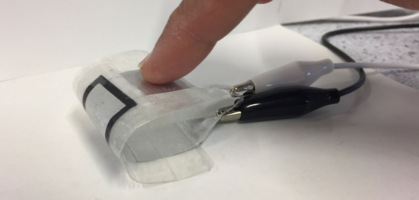
“It is applied like you would use a pen to write on a piece of paper,” said Yu. “We prepare several electronic materials and then use pens to dispense them. Coming out, it is liquid. But like ink on paper, it dries very quickly.”

Wearable bioelectronics – in the form of soft, flexible patches attached to the skin – have become an important way to monitor, prevent and treat illness and injury by tracking physiological information from the wearer. But even the most flexible wearables are limited by motion artifacts, or the difficulty that arises in collecting data when the sensor doesn’t move precisely with the skin.

The drawn-on-skin electronics can be customized to collect different types of information, and Yu said it is expected to be especially useful in situations where it’s not possible to access sophisticated equipment, including on a battleground.

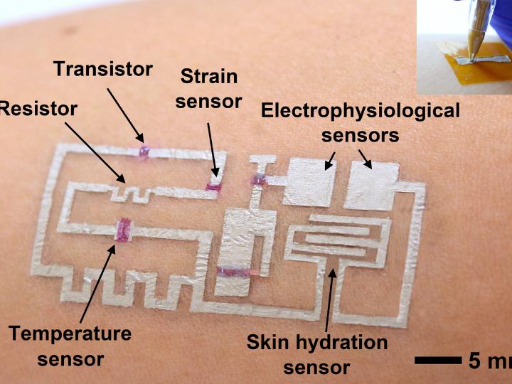
The electronics are able to track muscle signals, heart rate, temperature and skin hydration, among other physical data, he said. The researchers also reported that the drawn-on-skin electronics have demonstrated the ability to accelerate healing of wounds.

In addition to Yu, researchers involved in the project include Faheem Ershad, Anish Thukral, Phillip Comeaux, Yuntao Lu, Hyunseok Shim, Kyoseung Sim, Nam-In Kim, Zhoulyu Rao, Ross Guevara, Luis Contreras, Fengjiao Pan, Yongcao Zhang, Ying-Shi Guan, Pinyi Yang, Xu Wang and Peng Wang, all from the University of Houston, and Jiping Yue and Xiaoyang Wu from the University of Chicago.

The drawn-on-skin electronics are actually comprised of three inks, serving as a conductor, semiconductor and dielectric.

“Electronic inks, including conductors, semiconductors, and dielectrics, are drawn on-demand in a freeform manner to develop devices, such as transistors, strain sensors, temperature sensors, heaters, skin hydration sensors, and electrophysiological sensors,” the researchers wrote.

This research is supported by the Office of Naval Research and National Institutes of Health.

Caption: A new form of electronics known as “drawn-on-skin electronics” allows multifunctional sensors and circuits to be drawn on the skin with an ink pen. Credit: University of Houston

Here’s a link to and a citation for the paper,

Ultra-conformal drawn-on-skin electronics for multifunctional motion artifact-free sensing and point-of-care treatment by Faheem Ershad, Anish Thukral, Jiping Yue, Phillip Comeaux, Yuntao Lu, Hyunseok Shim, Kyoseung Sim, Nam-In Kim, Zhoulyu Rao, Ross Guevara, Luis Contreras, Fengjiao Pan, Yongcao Zhang, Ying-Shi Guan, Pinyi Yang, Xu Wang, Peng Wang, Xiaoyang Wu & Cunjiang Yu. Nature Communications volume 11, Article number: 3823 (2020) DOI: https://doi.org/10.1038/s41467-020-17619-1

This paper is open access.

New capacitor for better wearable electronics?

Supercapacitors are a predictable source of scientific interest and excitement. The latest entry in the ‘supercapacitor stakes’ is from a Russian/Finnish/US team according to a June 11, 2020 Skoltech (Skolkovo Institute of Science and Technology) press release (also on EurekAlert),

Researchers from Skoltech [Russia], Aalto University [Finland] and Massachusetts Institute of Technology [MIT; US] have designed a high-performance, low-cost, environmentally friendly, and stretchable supercapacitor that can potentially be used in wearable electronics. The paper was published in the Journal of Energy Storage.

Supercapacitors, with their high power density, fast charge-discharge rates, long cycle life, and cost-effectiveness, are a promising power source for everything from mobile and wearable electronics to electric vehicles. However, combining high energy density, safety, and eco-friendliness in one supercapacitor suitable for small devices has been rather challenging.

“Usually, organic solvents are used to increase the energy density. These are hazardous, not environmentally friendly, and they reduce the power density compared to aqueous electrolytes with higher conductivity,” says Professor Tanja Kallio from Aalto University, a co-author of the paper.

The researchers proposed a new design for a “green” and simple-to-fabricate supercapacitor. It consists of a solid-state material based on nitrogen-doped graphene flake electrodes distributed in the NaCl-containing hydrogel electrolyte. This structure is sandwiched between two single-walled carbon nanotube film current collectors, which provides stretchability. Hydrogel in the supercapacitor design enables compact packing and high energy density and allows them to use the environmentally friendly electrolyte.

The scientists managed to improve the volumetric capacitive performance, high energy density and power density for the prototype over analogous supercapacitors described in previous research. “We fabricated a prototype with unchanged performance under the 50% strain after a thousand stretching cycles. To ensure lower cost and better environmental performance, we used a NaCl-based electrolyte. Still the fabrication cost can be lowered down by implementation of 3D printing or other advanced fabrication techniques,” concluded Skoltech professor Albert Nasibulin.

Here’s a link to and a citation for the paper,

Superior environmentally friendly stretchable supercapacitor based on nitrogen-doped graphene/hydrogel and single-walled carbon nanotubes by Evgeniia Gilshtein, Cristina Flox, Farhan S.M. Ali, Bahareh Mehrabimatin, Fedor S.Fedorov, Shaoting Lin, Xuanhe Zhao, Albert G. Nasibulin, Tanja Kallio. Journal of Energy Storage Volume 30, August 2020, 101505 DOI: https://doi.org/10.1016/j.est.2020.101505

This paper is behind a paywall.

I’m trying to remember if I’ve ever before seen a material that combines graphene and single-walled carbon nanotubes (SWCNTs). Anyway, here’s an image the researchers are using illustrate their work,

Caption: This is an outline of the new supercapacitor. Credit: Pavel Odinev / Skoltech

Using light to manipulate neurons

There are three (or more?) possible applications including neuromorphic computing for this new optoelectronic technology which is based on black phophorus. A July 16, 2019 news item on Nanowerk announces the research,

Researchers from RMIT University [Australia] drew inspiration from an emerging tool in biotechnology – optogenetics – to develop a device that replicates the way the brain stores and loses information.

Optogenetics allows scientists to delve into the body’s electrical system with incredible precision, using light to manipulate neurons so that they can be turned on or off.

The new chip is based on an ultra-thin material that changes electrical resistance in response to different wavelengths of light, enabling it to mimic the way that neurons work to store and delete information in the brain.

Caption: The new chip is based on an ultra-thin material that changes electrical resistance in response to different wavelengths of light. Credit: RMIT University

A July 17, 2019 RMIT University press release (also on EurekAlert but published on July 16, 2019), which originated the news item, expands on the theme,

Research team leader Dr Sumeet Walia said the technology moves us closer towards artificial intelligence (AI) that can harness the brain’s full sophisticated functionality.

“Our optogenetically-inspired chip imitates the fundamental biology of nature’s best computer – the human brain,” Walia said.

“Being able to store, delete and process information is critical for computing, and the brain does this extremely efficiently.

“We’re able to simulate the brain’s neural approach simply by shining different colours onto our chip.

“This technology takes us further on the path towards fast, efficient and secure light-based computing.

“It also brings us an important step closer to the realisation of a bionic brain – a brain-on-a-chip that can learn from its environment just like humans do.”

Dr Taimur Ahmed, lead author of the study published in Advanced Functional Materials, said being able to replicate neural behavior on an artificial chip offered exciting avenues for research across sectors.

“This technology creates tremendous opportunities for researchers to better understand the brain and how it’s affected by disorders that disrupt neural connections, like Alzheimer’s disease and dementia,” Ahmed said.

The researchers, from the Functional Materials and Microsystems Research Group at RMIT, have also demonstrated the chip can perform logic operations – information processing – ticking another box for brain-like functionality.

Developed at RMIT’s MicroNano Research Facility, the technology is compatible with existing electronics and has also been demonstrated on a flexible platform, for integration into wearable electronics.

How the chip works:

Neural connections happen in the brain through electrical impulses. When tiny energy spikes reach a certain threshold of voltage, the neurons bind together – and you’ve started creating a memory.

On the chip, light is used to generate a photocurrent. Switching between colors causes the current to reverse direction from positive to negative.

This direction switch, or polarity shift, is equivalent to the binding and breaking of neural connections, a mechanism that enables neurons to connect (and induce learning) or inhibit (and induce forgetting).

This is akin to optogenetics, where light-induced modification of neurons causes them to either turn on or off, enabling or inhibiting connections to the next neuron in the chain.

To develop the technology, the researchers used a material called black phosphorus (BP) that can be inherently defective in nature.

This is usually a problem for optoelectronics, but with precision engineering the researchers were able to harness the defects to create new functionality.

“Defects are usually looked on as something to be avoided, but here we’re using them to create something novel and useful,” Ahmed said.

“It’s a creative approach to finding solutions for the technical challenges we face.”

Here’s a link and a citation for the paper,

Multifunctional Optoelectronics via Harnessing Defects in Layered Black Phosphorus by Taimur Ahmed, Sruthi Kuriakose, Sherif Abbas,, Michelle J. S. Spencer, Md. Ataur Rahman, Muhammad Tahir, Yuerui Lu, Prashant Sonar, Vipul Bansal, Madhu Bhaskaran, Sharath Sriram, Sumeet Walia. Advanced Functional Materials DOI: https://doi.org/10.1002/adfm.201901991 First published (online): 17 July 2019

This paper is behind a paywall.

If only AI had a brain (a Wizard of Oz reference?)

The title, which I’ve borrowed from the news release, is the only Wizard of Oz reference that I can find but it works so well, you don’t really need anything more.

Moving onto the news, a July 23, 2018 news item on phys.org announces new work on developing an artificial synapse (Note: A link has been removed),

Digital computation has rendered nearly all forms of analog computation obsolete since as far back as the 1950s. However, there is one major exception that rivals the computational power of the most advanced digital devices: the human brain.

The human brain is a dense network of neurons. Each neuron is connected to tens of thousands of others, and they use synapses to fire information back and forth constantly. With each exchange, the brain modulates these connections to create efficient pathways in direct response to the surrounding environment. Digital computers live in a world of ones and zeros. They perform tasks sequentially, following each step of their algorithms in a fixed order.

A team of researchers from Pitt’s [University of Pittsburgh] Swanson School of Engineering have developed an “artificial synapse” that does not process information like a digital computer but rather mimics the analog way the human brain completes tasks. Led by Feng Xiong, assistant professor of electrical and computer engineering, the researchers published their results in the recent issue of the journal Advanced Materials (DOI: 10.1002/adma.201802353). His Pitt co-authors include Mohammad Sharbati (first author), Yanhao Du, Jorge Torres, Nolan Ardolino, and Minhee Yun.

A July 23, 2018 University of Pittsburgh Swanson School of Engineering news release (also on EurekAlert), which originated the news item, provides further information,

“The analog nature and massive parallelism of the brain are partly why humans can outperform even the most powerful computers when it comes to higher order cognitive functions such as voice recognition or pattern recognition in complex and varied data sets,” explains Dr. Xiong.

An emerging field called “neuromorphic computing” focuses on the design of computational hardware inspired by the human brain. Dr. Xiong and his team built graphene-based artificial synapses in a two-dimensional honeycomb configuration of carbon atoms. Graphene’s conductive properties allowed the researchers to finely tune its electrical conductance, which is the strength of the synaptic connection or the synaptic weight. The graphene synapse demonstrated excellent energy efficiency, just like biological synapses.

In the recent resurgence of artificial intelligence, computers can already replicate the brain in certain ways, but it takes about a dozen digital devices to mimic one analog synapse. The human brain has hundreds of trillions of synapses for transmitting information, so building a brain with digital devices is seemingly impossible, or at the very least, not scalable. Xiong Lab’s approach provides a possible route for the hardware implementation of large-scale artificial neural networks.

According to Dr. Xiong, artificial neural networks based on the current CMOS (complementary metal-oxide semiconductor) technology will always have limited functionality in terms of energy efficiency, scalability, and packing density. “It is really important we develop new device concepts for synaptic electronics that are analog in nature, energy-efficient, scalable, and suitable for large-scale integrations,” he says. “Our graphene synapse seems to check all the boxes on these requirements so far.”

With graphene’s inherent flexibility and excellent mechanical properties, these graphene-based neural networks can be employed in flexible and wearable electronics to enable computation at the “edge of the internet”–places where computing devices such as sensors make contact with the physical world.

“By empowering even a rudimentary level of intelligence in wearable electronics and sensors, we can track our health with smart sensors, provide preventive care and timely diagnostics, monitor plants growth and identify possible pest issues, and regulate and optimize the manufacturing process–significantly improving the overall productivity and quality of life in our society,” Dr. Xiong says.

The development of an artificial brain that functions like the analog human brain still requires a number of breakthroughs. Researchers need to find the right configurations to optimize these new artificial synapses. They will need to make them compatible with an array of other devices to form neural networks, and they will need to ensure that all of the artificial synapses in a large-scale neural network behave in the same exact manner. Despite the challenges, Dr. Xiong says he’s optimistic about the direction they’re headed.

“We are pretty excited about this progress since it can potentially lead to the energy-efficient, hardware implementation of neuromorphic computing, which is currently carried out in power-intensive GPU clusters. The low-power trait of our artificial synapse and its flexible nature make it a suitable candidate for any kind of A.I. device, which would revolutionize our lives, perhaps even more than the digital revolution we’ve seen over the past few decades,” Dr. Xiong says.

There is a visual representation of this artificial synapse,

Caption: Pitt engineers built a graphene-based artificial synapse in a two-dimensional, honeycomb configuration of carbon atoms that demonstrated excellent energy efficiency comparable to biological synapses Credit: Swanson School of Engineering

Here’s a link to and a citation for the paper,

Low‐Power, Electrochemically Tunable Graphene Synapses for Neuromorphic Computing by Mohammad Taghi Sharbati, Yanhao Du, Jorge Torres, Nolan D. Ardolino, Minhee Yun, Feng Xiong. Advanced Materials DOP: https://doi.org/10.1002/adma.201802353 First published [online]: 23 July 2018

This paper is behind a paywall.

I did look at the paper and if I understand it rightly, this approach is different from the memristor-based approaches that I have so often featured here. More than that I cannot say.

Finally, the Wizard of Oz song ‘If I Only Had a Brain’,

New semiconductor material from pigment produced by fungi?

Chlorociboria Aeruginascens fungus on a tree log. (Image: Oregon State University)

Apparently the pigment derived from the fungi you see in the above picture is used by visual artists and, perhaps soon, will be used by electronics manufacturers. From a June 5, 2018 news item on Nanowerk,

Researchers at Oregon State University are looking at a highly durable organic pigment, used by humans in artwork for hundreds of years, as a promising possibility as a semiconductor material.

Findings suggest it could become a sustainable, low-cost, easily fabricated alternative to silicon in electronic or optoelectronic applications where the high-performance capabilities of silicon aren’t required.

Optoelectronics is technology working with the combined use of light and electronics, such as solar cells, and the pigment being studied is xylindein.

A June 5, 2018 Oregon State University news release by Steve Lundeberg, which originated the news item, expands on the theme,

“Xylindein is pretty, but can it also be useful? How much can we squeeze out of it?” said Oregon State University [OSU] physicist Oksana Ostroverkhova. “It functions as an electronic material but not a great one, but there’s optimism we can make it better.”

Xylindien is secreted by two wood-eating fungi in the Chlorociboria genus. Any wood that’s infected by the fungi is stained a blue-green color, and artisans have prized xylindein-affected wood for centuries.

The pigment is so stable that decorative products made half a millennium ago still exhibit its distinctive hue. It holds up against prolonged exposure to heat, ultraviolet light and electrical stress.

“If we can learn the secret for why those fungi-produced pigments are so stable, we could solve a problem that exists with organic electronics,” Ostroverkhova said. “Also, many organic electronic materials are too expensive to produce, so we’re looking to do something inexpensively in an ecologically friendly way that’s good for the economy.”

With current fabrication techniques, xylindein tends to form non-uniform films with a porous, irregular, “rocky” structure.

“There’s a lot of performance variation,” she said. “You can tinker with it in the lab, but you can’t really make a technologically relevant device out of it on a large scale. But we found a way to make it more easily processed and to get a decent film quality.”

Ostroverkhova and collaborators in OSU’s colleges of Science and Forestry blended xylindein with a transparent, non-conductive polymer, poly(methyl methacrylate), abbreviated to PMMA and sometimes known as acrylic glass. They drop-cast solutions both of pristine xylindein and a xlyindein-PMMA blend onto electrodes on a glass substrate for testing.

They found the non-conducting polymer greatly improved the film structure without a detrimental effect on xylindein’s electrical properties. And the blended films actually showed better photosensitivity.

“Exactly why that happened, and its potential value in solar cells, is something we’ll be investigating in future research,” Ostroverkhova said. “We’ll also look into replacing the polymer with a natural product – something sustainable made from cellulose. We could grow the pigment from the cellulose and be able to make a device that’s all ready to go.

“Xylindein will never beat silicon, but for many applications, it doesn’t need to beat silicon,” she said. “It could work well for depositing onto large, flexible substrates, like for making wearable electronics.”

This research, whose findings were recently published in MRS Advances, represents the first use of a fungus-produced material in a thin-film electrical device.

“And there are a lot more of the materials,” Ostroverkhova said. “This is just first one we’ve explored. It could be the beginning of a whole new class of organic electronic materials.”

Here’s a link to and a citation for the paper,

Fungi-Derived Pigments for Sustainable Organic (Opto)Electronics by Gregory Giesbers, Jonathan Van Schenck, Sarath Vega Gutierrez, Sara Robinson. MRS Advances https://doi.org/10.1557/adv.2018.446 Published online: 21 May 2018

This paper is behind a paywall.

The new knitting: electronics and batteries

Researchers from China have developed a new type of yarn for flexible electronics. A March 28, 2018 news item on Nanowerk announces the work, (Note: A link has been removed),

When someone thinks about knitting, they usually don’t conjure up an image of sweaters and scarves made of yarn that can power watches and lights. But that’s just what one group is reporting in ACS Nano (“Waterproof and Tailorable Elastic Rechargeable Yarn Zinc Ion Batteries by a Cross-Linked Polyacrylamide Electrolyte”). They have developed a rechargeable yarn battery that is waterproof and flexible. It also can be cut into pieces and still work.

A March 28, 2018 2018 American Chemical Society (ACS) news release (also on EurekAlert), which originated the news item, expands on the theme (Note: Links have been removed),

Most people are familiar with smartwatches, but for wearable electronics to progress, scientists will need to overcome the challenge of creating a device that is deformable, durable, versatile and wearable while still holding and maintaining a charge. One dimensional fiber or yarn has shown promise, since it is tiny, flexible and lightweight. Previous studies have had some success combining one-dimensional fibers with flexible Zn-MnO2 batteries, but many of these lose charge capacity and are not rechargeable. So, Chunyi Zhi and colleagues wanted to develop a rechargeable yarn zinc-ion battery that would maintain its charge capacity, while being waterproof and flexible.

The group twisted carbon nanotube fibers into a yarn, then coated one piece of yarn with zinc to form an anode, and another with magnesium oxide to form a cathode. These two pieces were then twisted like a double helix and coated with a polyacrylamide electrolyte and encased in silicone. Upon testing, the yarn zinc-ion battery was stable, had a high charge capacity and was rechargeable and waterproof. In addition, the material could be knitted and stretched. It also could be cut into several pieces, each of which could power a watch. In a proof-of-concept demonstration, eight pieces of the cut yarn battery were woven into a long piece that could power a belt containing 100 light emitting diodes (known as LEDs) and an electroluminescent panel.

The authors acknowledge funding from the National Natural Science Foundation of China and the Research Grants Council of Hong Kong Joint Research Scheme, City University of Hong Kong and the Sichuan Provincial Department of Science & Technology.

Here’s an image the researchers have used to illustrate their work,


Courtesy: American Chemical Society

Here’s a link to and a citation for the paper,

Waterproof and Tailorable Elastic Rechargeable Yarn Zinc Ion Batteries by a Cross-Linked Polyacrylamide Electrolyte by Hongfei Li, Zhuoxin Liu, Guojin Liang, Yang Huang, Yan Huang, Minshen Zhu, Zengxia Pe, Qi Xue, Zijie Tang, Yukun Wang, Baohua Li, and Chunyi Zhi. ACS Nano, Article ASAP DOI: 10.1021/acsnano.7b09003 Publication Date (Web): March 28, 2018

Copyright © 2018 American Chemical Society

This paper is behind a paywall.

Do you want that coffee with some graphene on toast?

These scientists are excited:

For those who prefer text, here’s the Rice University Feb. 13, 2018 news release (received via email and available online here and on EurekAlert here) Note: Links have been removed),

Rice University scientists who introduced laser-induced graphene (LIG) have enhanced their technique to produce what may become a new class of edible electronics.

The Rice lab of chemist James Tour, which once turned Girl Scout cookies into graphene, is investigating ways to write graphene patterns onto food and other materials to quickly embed conductive identification tags and sensors into the products themselves.

“This is not ink,” Tour said. “This is taking the material itself and converting it into graphene.”

The process is an extension of the Tour lab’s contention that anything with the proper carbon content can be turned into graphene. In recent years, the lab has developed and expanded upon its method to make graphene foam by using a commercial laser to transform the top layer of an inexpensive polymer film.

The foam consists of microscopic, cross-linked flakes of graphene, the two-dimensional form of carbon. LIG can be written into target materials in patterns and used as a supercapacitor, an electrocatalyst for fuel cells, radio-frequency identification (RFID) antennas and biological sensors, among other potential applications.

The new work reported in the American Chemical Society journal ACS Nano demonstrated that laser-induced graphene can be burned into paper, cardboard, cloth, coal and certain foods, even toast.

“Very often, we don’t see the advantage of something until we make it available,” Tour said. “Perhaps all food will have a tiny RFID tag that gives you information about where it’s been, how long it’s been stored, its country and city of origin and the path it took to get to your table.”

He said LIG tags could also be sensors that detect E. coli or other microorganisms on food. “They could light up and give you a signal that you don’t want to eat this,” Tour said. “All that could be placed not on a separate tag on the food, but on the food itself.”

Multiple laser passes with a defocused beam allowed the researchers to write LIG patterns into cloth, paper, potatoes, coconut shells and cork, as well as toast. (The bread is toasted first to “carbonize” the surface.) The process happens in air at ambient temperatures.

“In some cases, multiple lasing creates a two-step reaction,” Tour said. “First, the laser photothermally converts the target surface into amorphous carbon. Then on subsequent passes of the laser, the selective absorption of infrared light turns the amorphous carbon into LIG. We discovered that the wavelength clearly matters.”

The researchers turned to multiple lasing and defocusing when they discovered that simply turning up the laser’s power didn’t make better graphene on a coconut or other organic materials. But adjusting the process allowed them to make a micro supercapacitor in the shape of a Rice “R” on their twice-lased coconut skin.

Defocusing the laser sped the process for many materials as the wider beam allowed each spot on a target to be lased many times in a single raster scan. That also allowed for fine control over the product, Tour said. Defocusing allowed them to turn previously unsuitable polyetherimide into LIG.

“We also found we could take bread or paper or cloth and add fire retardant to them to promote the formation of amorphous carbon,” said Rice graduate student Yieu Chyan, co-lead author of the paper. “Now we’re able to take all these materials and convert them directly in air without requiring a controlled atmosphere box or more complicated methods.”

The common element of all the targeted materials appears to be lignin, Tour said. An earlier study relied on lignin, a complex organic polymer that forms rigid cell walls, as a carbon precursor to burn LIG in oven-dried wood. Cork, coconut shells and potato skins have even higher lignin content, which made it easier to convert them to graphene.

Tour said flexible, wearable electronics may be an early market for the technique. “This has applications to put conductive traces on clothing, whether you want to heat the clothing or add a sensor or conductive pattern,” he said.

Rice alumnus Ruquan Ye is co-lead author of the study. Co-authors are Rice graduate student Yilun Li and postdoctoral fellow Swatantra Pratap Singh and Professor Christopher Arnusch of Ben-Gurion University of the Negev, Israel. Tour is the T.T. and W.F. Chao Chair in Chemistry as well as a professor of computer science and of materials science and nanoengineering at Rice.

The Air Force Office of Scientific Research supported the research.

Here’s a link to and a citation for the paper,

Laser-Induced Graphene by Multiple Lasing: Toward Electronics on Cloth, Paper, and Food by Yieu Chyan, Ruquan Ye†, Yilun Li, Swatantra Pratap Singh, Christopher J. Arnusch, and James M. Tour. ACS Nano DOI: 10.1021/acsnano.7b08539 Publication Date (Web): February 13, 2018

Copyright © 2018 American Chemical Society

This paper is behind a paywall.

h/t Feb. 13, 2018 news item on Nanowerk

Liquid circuitry, shape-shifting fluids and more

I’d have to see it to believe it but researchers at the US Dept. of Energy (DOE) Lawrence Berkeley National Laboratory (LBNL) have developed a new kind of ‘bijel’ which would allow for some pretty nifty robotics. From a Sept. 25, 2017 news item on ScienceDaily,

A new two-dimensional film, made of polymers and nanoparticles and developed by researchers at the Department of Energy’s Lawrence Berkeley National Laboratory (Berkeley Lab), can direct two different non-mixing liquids into a variety of exotic architectures. This finding could lead to soft robotics, liquid circuitry, shape-shifting fluids, and a host of new materials that use soft, rather than solid, substances.

The study, reported today in the journal Nature Nanotechnology, presents the newest entry in a class of substances known as bicontinuous jammed emulsion gels, or bijels, which hold promise as a malleable liquid that can support catalytic reactions, electrical conductivity, and energy conversion.

A Sept. 25, 2017 LBNL news release (also on EurekAlert), which originated the news item, expands on the theme,

Bijels are typically made of immiscible, or non-mixing, liquids. People who shake their bottle of vinaigrette before pouring the dressing on their salad are familiar with such liquids. As soon as the shaking stops, the liquids start to separate again, with the lower density liquid – often oil – rising to the top.

Trapping, or jamming, particles where these immiscible liquids meet can prevent the liquids from completely separating, stabilizing the substance into a bijel. What makes bijels remarkable is that, rather than just making the spherical droplets that we normally see when we try to mix oil and water, the particles at the interface shape the liquids into complex networks of interconnected fluid channels.

Bijels are notoriously difficult to make, however, involving exact temperatures at precisely timed stages. In addition, the liquid channels are normally more than 5 micrometers across, making them too large to be useful in energy conversion and catalysis.

“Bijels have long been of interest as next-generation materials for energy applications and chemical synthesis,” said study lead author Caili Huang. “The problem has been making enough of them, and with features of the right size. In this work, we crack that problem.”

Huang started the work as a graduate student with Thomas Russell, the study’s principal investigator, at Berkeley Lab’s Materials Sciences Division, and he continued the project as a postdoctoral researcher at DOE’s Oak Ridge National Laboratory.

Creating a new bijel recipe

The method described in this new study simplifies the bijel process by first using specially coated particles about 10-20 nanometers in diameter. The smaller-sized particles line the liquid interfaces much more quickly than the ones used in traditional bijels, making the smaller channels that are highly valued for applications.

Illustration shows key stages of bijel formation. Clockwise from top left, two non-mixing liquids are shown. Ligands (shown in yellow) with amine groups are dispersed throughout the oil or solvent, and nanoparticles coated with carboxylic acids (shown as blue dots) are scattered in the water. With vigorous shaking, the nanoparticles and ligands form a “supersoap” that gets trapped at the interface of the two liquids. The bottom panel is a magnified view of the jammed nanoparticle supersoap. (Credit: Caili Huang/ORNL)

“We’ve basically taken liquids like oil and water and given them a structure, and it’s a structure that can be changed,” said Russell, a visiting faculty scientist at Berkeley Lab. “If the nanoparticles are responsive to electrical, magnetic, or mechanical stimuli, the bijels can become reconfigurable and re-shaped on demand by an external field.”

The researchers were able to prepare new bijels from a variety of common organic, water-insoluble solvents, such as toluene, that had ligands dissolved in it, and deionized water, which contained the nanoparticles. To ensure thorough mixing of the liquids, they subjected the emulsion to a vortex spinning at 3,200 revolutions per minute.

“This extreme shaking creates a whole bunch of new places where these particles and polymers can meet each other,” said study co-author Joe Forth, a postdoctoral fellow at Berkeley Lab’s Materials Sciences Division. “You’re synthesizing a lot of this material, which is in effect a thin, 2-D coating of the liquid surfaces in the system.”

The liquids remained a bijel even after one week, a sign of the system’s stability.

Russell, who is also a professor of polymer science and engineering at the University of Massachusetts-Amherst, added that these shape-shifting characteristics would be valuable in microreactors, microfluidic devices, and soft actuators.

Nanoparticle supersoap

Nanoparticles had not been seriously considered in bijels before because their small size made them hard to trap in the liquid interface. To resolve that problem, the researchers coated nano-sized particles with carboxylic acids and put them in water. They then took polymers with an added amine group – a derivative of ammonia – and dissolved them in the toluene.

At left is a vial of bijel stabilized with nanoparticle surfactants. On the right is the same vial after a week of inversion, showing that the nanoparticle kept the liquids from moving. (Credit: Caili Huang/ORNL)

This configuration took advantage of the amine group’s affinity to water, a characteristic that is comparable to surfactants, like soap. Their nanoparticle “supersoap” was designed so that the nanoparticles join ligands, forming an octopus-like shape with a polar head and nonpolar legs that get jammed at the interface, the researchers said.

“Bijels are really a new material, and also excitingly weird in that they are kinetically arrested in these unusual configurations,” said study co-author Brett Helms, a staff scientist at Berkeley Lab’s Molecular Foundry. “The discovery that you can make these bijels with simple ingredients is a surprise. We all have access to oils and water and nanocrystals, allowing broad tunability in bijel properties. This platform also allows us to experiment with new ways to control their shape and function since they are both responsive and reconfigurable.”

The nanoparticles were made of silica, but the researchers noted that in previous studies they used graphene and carbon nanotubes to form nanoparticle surfactants.

“The key is that the nanoparticles can be made of many materials,” said Russell.  “The most important thing is what’s on the surface.”

This is an animation of the bijel

3-D rendering of the nanoparticle bijel taken by confocal microscope. (Credit: Caili Huang/ORNL [Oak Ridge National Laboratory] and Joe Forth/Berkeley Lab)

Here’s a link to and a citation for the paper,

Bicontinuous structured liquids with sub-micrometre domains using nanoparticle surfactants by Caili Huang, Joe Forth, Weiyu Wang, Kunlun Hong, Gregory S. Smith, Brett A. Helms & Thomas P. Russell. Nature Nanotechnology (2017) doi:10.1038/nnano.2017.182 25 September 2017

This paper is behind a paywall.

A flexible, organic battery from Northern Ireland

A team from Northern Ireland seems to have made a splash in the race to develop a flexible, environmentally friendly battery. From a Sept. 13, 2017 news item on phys.org,

Experts at Queen’s University Belfast have designed a flexible and organic alternative to the rigid batteries that power up medical implants.

Currently, devices such as pacemakers and defibrillators are fitted with rigid and metal based batteries, which can cause patient discomfort.

Dr Geetha Srinivasan and a team of young researchers from Queen’s University Ionic Liquid Laboratories (QUILL) Research Centre, have now developed a flexible supercapacitor with a longer cycle life, which could power body sensors.

Courtesy: Queen’s University Belfast

A Sept. 13, 2017 Queen’s University Belfast press release (also on EurekAlert), which originated the news item, delves further,

The flexible device is made up of non-flammable electrolytes and organic composites, which are safe to the human body. It can also be easily decomposed without incurring the major costs associated with recycling or disposing off metal based batteries.

The findings, which have been published in Energy Technology and Green Chemistry, show that the device could be manufactured using readily available natural feedstock, rather than sophisticated and expensive metals or semiconductors.

Dr Srinivasan explains: “In modern society, we all increasingly depend on portable electronics such as smartphones and laptops in our everyday lives and this trend has spread to other important areas such as healthcare devices.

“In medical devices such as pacemakers and defibrillators there are two implants, one which is fitted in the heart and another which holds the metal based, rigid batteries – this is implanted under the skin.

“The implant under the skin is wired to the device and can cause patients discomfort as it is rubs against the skin. For this reason batteries need to be compatible to the human body and ideally we would like them to be flexible so that they can adapt to body shapes.”

Dr Srinivasan adds: “At Queen’s University Belfast we have designed a flexible energy storage device, which consists of conducting polymer – biopolymer composites as durable electrodes and ionic liquids as safer electrolytes.

“The device we have created has a longer life-cycle, is non-flammable, has no leakage issues and above all, it is more flexible for placing within the body.”

Environmentally friendly

While the findings show that there are many advantages in the medical world, the organic storage device could also provide solutions in wearable electronics and portable electronic devices, making these more flexible.

Ms Marta Lorenzo, PhD researcher on the project at Queen’s University Belfast, commented: “Although this research could be a potential solution to a global problem, the actual supercapacitor assembly is a straightforward process.”

Dr Srinivasan says: “There is also opportunity to fabricate task-specific supercapacitors. This means that their properties can be tuned and also manufactured using environmentally friendly methods, which is important if they are to be produced on a large scale, for example in powering portable personal electronic devices.”

Here are links and citations to the two papers mentioned in the press release,

Durable Flexible Supercapacitors Utilizing the Multifunctional Role of Ionic Liquids by Marta Lorenzo and Dr Geetha Srinivasan. Energy Technology. DOI: 10.1002/ente.201700407 First published: 23 August 2017

Intrinsically flexible electronic materials for smart device applications by Marta Lorenzo, Biyun Zhu, and Geetha Srinivasan. Green Chem., 2016,18, 3513-3517 DOI: 10.1039/C6GC00826G First published on 20 May 2016

The first paper is open access and the second paper is behind a paywall.

Vampire nanogenerators: 2017

Researchers have been working on ways to harvest energy from bloodstreams. I last wrote about this type of research in an April 3, 2009 posting about ‘vampire batteries ‘(for use in pacemakers). The latest work according to a Sept. 8, 2017 news item on Nanowerk comes from China,

Men build dams and huge turbines to turn the energy of waterfalls and tides into electricity. To produce hydropower on a much smaller scale, Chinese scientists have now developed a lightweight power generator based on carbon nanotube fibers suitable to convert even the energy of flowing blood in blood vessels into electricity. They describe their innovation in the journal Angewandte Chemie (“A One-Dimensional Fluidic Nanogenerator with a High Power Conversion Efficiency”)

A Sept. 8, 2017 Wiley Publishing news release (also on EurekAlert), which originated the news item, expands on the theme,

For thousands of years, people have used the energy of flowing or falling water for their purposes, first to power mechanical engines such as watermills, then to generate electricity by exploiting height differences in the landscape or sea tides. Using naturally flowing water as a sustainable power source has the advantage that there are (almost) no dependencies on weather or daylight. Even flexible, minute power generators that make use of the flow of biological fluids are conceivable. How such a system could work is explained by a research team from Fudan University in Shanghai, China. Huisheng Peng and his co-workers have developed a fiber with a thickness of less than a millimeter that generates electrical power when surrounded by flowing saline solution—in a thin tube or even in a blood vessel.

The construction principle of the fiber is quite simple. An ordered array of carbon nanotubes was continuously wrapped around a polymeric core. Carbon nanotubes are well known to be electroactive and mechanically stable; they can be spun and aligned in sheets. In the as-prepared electroactive threads, the carbon nanotube sheets coated the fiber core with a thickness of less than half a micron. For power generation, the thread or “fiber-shaped fluidic nanogenerator” (FFNG), as the authors call it, was connected to electrodes and immersed into flowing water or simply repeatedly dipped into a saline solution. “The electricity was derived from the relative movement between the FFNG and the solution,” the scientists explained. According to the theory, an electrical double layer is created around the fiber, and then the flowing solution distorts the symmetrical charge distribution, generating an electricity gradient along the long axis.

The power output efficiency of this system was high. Compared with other types of miniature energy-harvesting devices, the FFNG was reported to show a superior power conversion efficiency of more than 20%. Other advantages are elasticity, tunability, lightweight, and one-dimensionality, thus offering prospects of exciting technological applications. The FFNG can be made stretchable just by spinning the sheets around an elastic fiber substrate. If woven into fabrics, wearable electronics become thus a very interesting option for FFNG application. Another exciting application is the harvesting of electrical energy from the bloodstream for medical applications. First tests with frog nerves proved to be successful.

Here’s a link to and a citation for the paper,

A One-Dimensional Fluidic Nanogenerator with a High Power Conversion Efficiency by Yifan Xu, Dr. Peining Chen, Jing Zhang, Songlin Xie, Dr. Fang Wan, Jue Deng, Dr. Xunliang Cheng, Yajie Hu, Meng Liao, Dr. Bingjie Wang, Dr. Xuemei Sun, and Prof. Dr. Huisheng Peng. Angewandte Chemie International Edition DOI: 10.1002/anie.201706620 Version of Record online: 7 SEP 2017

© 2017 Wiley-VCH Verlag GmbH & Co. KGaA, Weinheim

This paper is behind a paywall.