Tag Archives: flexible electronics

A solar, self-charging supercapacitor for wearable technology

Ravinder Dahiya, Carlos García Núñez, and their colleagues at the University of Glasgow (Scotland) strike again (see my May 10, 2017 posting for their first ‘solar-powered graphene skin’ research announcement). Last time it was all about robots and prosthetics, this time they’ve focused on wearable technology according to a July 18, 2018 news item on phys.org,

A new form of solar-powered supercapacitor could help make future wearable technologies lighter and more energy-efficient, scientists say.

In a paper published in the journal Nano Energy, researchers from the University of Glasgow’s Bendable Electronics and Sensing Technologies (BEST) group describe how they have developed a promising new type of graphene supercapacitor, which could be used in the next generation of wearable health sensors.

A July 18, 2018 University of Glasgow press release, which originated the news item, explains further,

Currently, wearable systems generally rely on relatively heavy, inflexible batteries, which can be uncomfortable for long-term users. The BEST team, led by Professor Ravinder Dahiya, have built on their previous success in developing flexible sensors by developing a supercapacitor which could power health sensors capable of conforming to wearer’s bodies, offering more comfort and a more consistent contact with skin to better collect health data.

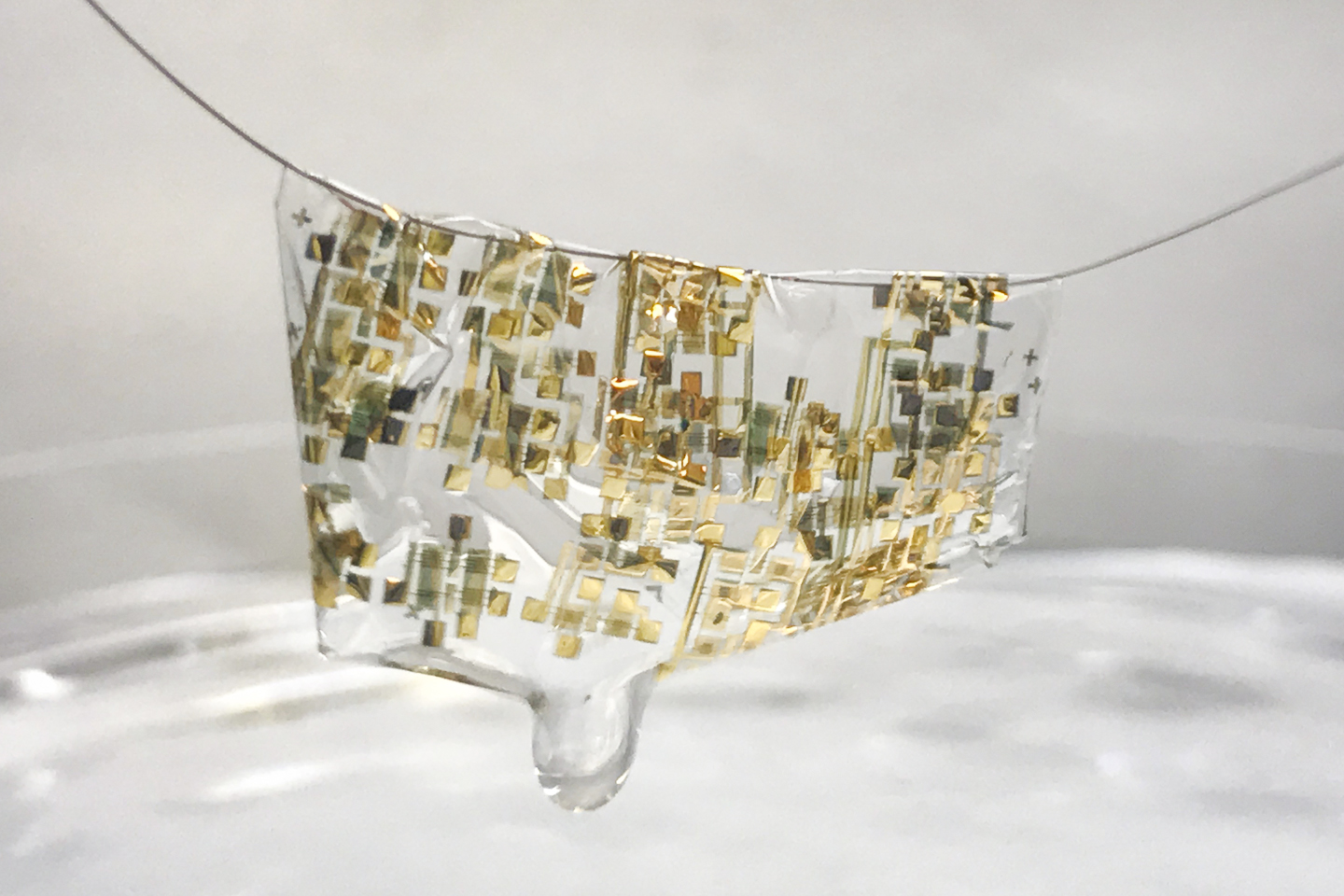
Their new supercapacitor uses layers of flexible, three-dimensional porous foam formed from graphene and silver to produce a device capable of storing and releasing around three times more power than any similar flexible supercapacitor. The team demonstrated the durability of the supercapacitor, showing that it provided power consistently across 25,000 charging and discharging cycles.

They have also found a way to charge the system by integrating it with flexible solar powered skin already developed by the BEST group, effectively creating an entirely self-charging system, as well as a pH sensor which uses wearer’s sweat to monitor their health.

Professor Dahiya said: “We’re very pleased by the progress this new form of solar-powered supercapacitor represents. A flexible, wearable health monitoring system which only requires exposure to sunlight to charge has a lot of obvious commercial appeal, but the underlying technology has a great deal of additional potential.

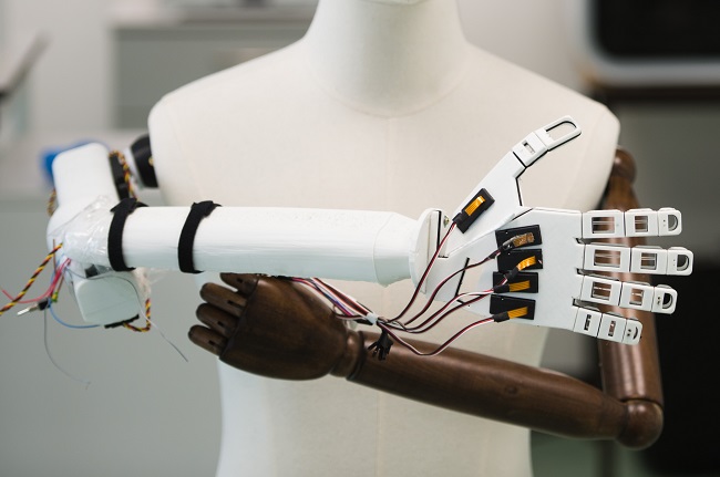
“This research could take the wearable systems for health monitoring to remote parts of the world where solar power is often the most reliable source of energy, and it could also increase the efficiency of hybrid electric vehicles. We’re already looking at further integrating the technology into flexible synthetic skin which we’re developing for use in advanced prosthetics.” [emphasis mine]

In addition to the team’s work on robots, prosthetics, and graphene ‘skin’ mentioned in the May 10, 2017 posting the team is working on a synthetic ‘brainy’ skin for which they have just received £1.5m funding from the Engineering and Physical Science Research Council (EPSRC).

Brainy skin

A July 3, 2018 University of Glasgow press release discusses the proposed work in more detail,

A robotic hand covered in ‘brainy skin’ that mimics the human sense of touch is being developed by scientists.

University of Glasgow’s Professor Ravinder Dahiya has plans to develop ultra-flexible, synthetic Brainy Skin that ‘thinks for itself’.

The super-flexible, hypersensitive skin may one day be used to make more responsive prosthetics for amputees, or to build robots with a sense of touch.

Brainy Skin reacts like human skin, which has its own neurons that respond immediately to touch rather than having to relay the whole message to the brain.

This electronic ‘thinking skin’ is made from silicon based printed neural transistors and graphene – an ultra-thin form of carbon that is only an atom thick, but stronger than steel.

The new version is more powerful, less cumbersome and would work better than earlier prototypes, also developed by Professor Dahiya and his Bendable Electronics and Sensing Technologies (BEST) team at the University’s School of Engineering.

His futuristic research, called neuPRINTSKIN (Neuromorphic Printed Tactile Skin), has just received another £1.5m funding from the Engineering and Physical Science Research Council (EPSRC).

Professor Dahiya said: “Human skin is an incredibly complex system capable of detecting pressure, temperature and texture through an array of neural sensors that carry signals from the skin to the brain.

“Inspired by real skin, this project will harness the technological advances in electronic engineering to mimic some features of human skin, such as softness, bendability and now, also sense of touch. This skin will not just mimic the morphology of the skin but also its functionality.

“Brainy Skin is critical for the autonomy of robots and for a safe human-robot interaction to meet emerging societal needs such as helping the elderly.”

Synthetic ‘Brainy Skin’ with sense of touch gets £1.5m funding. Photo of Professor Ravinder Dahiya

This latest advance means tactile data is gathered over large areas by the synthetic skin’s computing system rather than sent to the brain for interpretation.

With additional EPSRC funding, which extends Professor Dahiya’s fellowship by another three years, he plans to introduce tactile skin with neuron-like processing. This breakthrough in the tactile sensing research will lead to the first neuromorphic tactile skin, or ‘brainy skin.’

To achieve this, Professor Dahiya will add a new neural layer to the e-skin that he has already developed using printing silicon nanowires.

Professor Dahiya added: “By adding a neural layer underneath the current tactile skin, neuPRINTSKIN will add significant new perspective to the e-skin research, and trigger transformations in several areas such as robotics, prosthetics, artificial intelligence, wearable systems, next-generation computing, and flexible and printed electronics.”

The Engineering and Physical Sciences Research Council (EPSRC) is part of UK Research and Innovation, a non-departmental public body funded by a grant-in-aid from the UK government.

EPSRC is the main funding body for engineering and physical sciences research in the UK. By investing in research and postgraduate training, the EPSRC is building the knowledge and skills base needed to address the scientific and technological challenges facing the nation.

Its portfolio covers a vast range of fields from healthcare technologies to structural engineering, manufacturing to mathematics, advanced materials to chemistry. The research funded by EPSRC has impact across all sectors. It provides a platform for future UK prosperity by contributing to a healthy, connected, resilient, productive nation.

It’s fascinating to note how these pieces of research fit together for wearable technology and health monitoring and creating more responsive robot ‘skin’ and, possibly, prosthetic devices that would allow someone to feel again.

The latest research paper

Getting back the solar-charging supercapacitors mentioned in the opening, here’s a link to and a citation for the team’s latest research paper,

Flexible self-charging supercapacitor based on graphene-Ag-3D graphene foam electrodes by Libu Manjakka, Carlos García Núñez, Wenting Dang, Ravinder Dahiya. Nano Energy Volume 51, September 2018, Pages 604-612 DOI: https://doi.org/10.1016/j.nanoen.2018.06.072

This paper is open access.

The new knitting: electronics and batteries

Researchers from China have developed a new type of yarn for flexible electronics. A March 28, 2018 news item on Nanowerk announces the work, (Note: A link has been removed),

When someone thinks about knitting, they usually don’t conjure up an image of sweaters and scarves made of yarn that can power watches and lights. But that’s just what one group is reporting in ACS Nano (“Waterproof and Tailorable Elastic Rechargeable Yarn Zinc Ion Batteries by a Cross-Linked Polyacrylamide Electrolyte”). They have developed a rechargeable yarn battery that is waterproof and flexible. It also can be cut into pieces and still work.

A March 28, 2018 2018 American Chemical Society (ACS) news release (also on EurekAlert), which originated the news item, expands on the theme (Note: Links have been removed),

Most people are familiar with smartwatches, but for wearable electronics to progress, scientists will need to overcome the challenge of creating a device that is deformable, durable, versatile and wearable while still holding and maintaining a charge. One dimensional fiber or yarn has shown promise, since it is tiny, flexible and lightweight. Previous studies have had some success combining one-dimensional fibers with flexible Zn-MnO2 batteries, but many of these lose charge capacity and are not rechargeable. So, Chunyi Zhi and colleagues wanted to develop a rechargeable yarn zinc-ion battery that would maintain its charge capacity, while being waterproof and flexible.

The group twisted carbon nanotube fibers into a yarn, then coated one piece of yarn with zinc to form an anode, and another with magnesium oxide to form a cathode. These two pieces were then twisted like a double helix and coated with a polyacrylamide electrolyte and encased in silicone. Upon testing, the yarn zinc-ion battery was stable, had a high charge capacity and was rechargeable and waterproof. In addition, the material could be knitted and stretched. It also could be cut into several pieces, each of which could power a watch. In a proof-of-concept demonstration, eight pieces of the cut yarn battery were woven into a long piece that could power a belt containing 100 light emitting diodes (known as LEDs) and an electroluminescent panel.

The authors acknowledge funding from the National Natural Science Foundation of China and the Research Grants Council of Hong Kong Joint Research Scheme, City University of Hong Kong and the Sichuan Provincial Department of Science & Technology.

Here’s an image the researchers have used to illustrate their work,


Courtesy: American Chemical Society

Here’s a link to and a citation for the paper,

Waterproof and Tailorable Elastic Rechargeable Yarn Zinc Ion Batteries by a Cross-Linked Polyacrylamide Electrolyte by Hongfei Li, Zhuoxin Liu, Guojin Liang, Yang Huang, Yan Huang, Minshen Zhu, Zengxia Pe, Qi Xue, Zijie Tang, Yukun Wang, Baohua Li, and Chunyi Zhi. ACS Nano, Article ASAP DOI: 10.1021/acsnano.7b09003 Publication Date (Web): March 28, 2018

Copyright © 2018 American Chemical Society

This paper is behind a paywall.

Soft things for your brain

A March 5, 2018 news item on Nanowerk describes the latest stretchable electrode (Note: A link has been removed),

Klas Tybrandt, principal investigator at the Laboratory of Organic Electronics at Linköping University [Sweden], has developed new technology for long-term stable neural recording. It is based on a novel elastic material composite, which is biocompatible and retains high electrical conductivity even when stretched to double its original length.

The result has been achieved in collaboration with colleagues in Zürich and New York. The breakthrough, which is crucial for many applications in biomedical engineering, is described in an article published in the prestigious scientific journal Advanced Materials (“High-Density Stretchable Electrode Grids for Chronic Neural Recording”).

A March 5, 2018 Linköping University press release, which originated the news item, gives more detail but does not mention that the nanowires are composed of titanium dioxide (you can find additional details in the abstract for the paper; link and citation will be provided later in this posting)),

The coupling between electronic components and nerve cells is crucial not only to collect information about cell signalling, but also to diagnose and treat neurological disorders and diseases, such as epilepsy.

It is very challenging to achieve long-term stable connections that do not damage neurons or tissue, since the two systems, the soft and elastic tissue of the body and the hard and rigid electronic components, have completely different mechanical properties.

Stretchable soft electrodeThe soft electrode stretched to twice its length Photo credit: Thor Balkhed

“As human tissue is elastic and mobile, damage and inflammation arise at the interface with rigid electronic components. It not only causes damage to tissue; it also attenuates neural signals,” says Klas Tybrandt, leader of the Soft Electronics group at the Laboratory of Organic Electronics, Linköping University, Campus Norrköping.

New conductive material

Klas Tybrandt has developed a new conductive material that is as soft as human tissue and can be stretched to twice its length. The material consists of gold coated titanium dioxide nanowires, embedded into silicone rubber. The material is biocompatible – which means it can be in contact with the body without adverse effects – and its conductivity remains stable over time.

“The microfabrication of soft electrically conductive composites involves several challenges. We have developed a process to manufacture small electrodes that also preserves the biocompatibility of the materials. The process uses very little material, and this means that we can work with a relatively expensive material such as gold, without the cost becoming prohibitive,” says Klas Tybrandt.

The electrodes are 50 µm [microns or micrometres] in size and are located at a distance of 200 µm from each other. The fabrication procedure allows 32 electrodes to be placed onto a very small surface. The final probe, shown in the photograph, has a width of 3.2 mm and a thickness of 80 µm.

The soft microelectrodes have been developed at Linköping University and ETH Zürich, and researchers at New York University and Columbia University have subsequently implanted them in the brain of rats. The researchers were able to collect high-quality neural signals from the freely moving rats for 3 months. The experiments have been subject to ethical review, and have followed the strict regulations that govern animal experiments.

Important future applications

Klas Tybrandt, researcher at Laboratory for Organic ElectronicsKlas Tybrandt, researcher at Laboratory for Organic Electronics Photo credit: Thor Balkhed

“When the neurons in the brain transmit signals, a voltage is formed that the electrodes detect and transmit onwards through a tiny amplifier. We can also see which electrodes the signals came from, which means that we can estimate the location in the brain where the signals originated. This type of spatiotemporal information is important for future applications. We hope to be able to see, for example, where the signal that causes an epileptic seizure starts, a prerequisite for treating it. Another area of application is brain-machine interfaces, by which future technology and prostheses can be controlled with the aid of neural signals. There are also many interesting applications involving the peripheral nervous system in the body and the way it regulates various organs,” says Klas Tybrandt.

The breakthrough is the foundation of the research area Soft Electronics, currently being established at Linköping University, with Klas Tybrandt as principal investigator.
liu.se/soft-electronics

A video has been made available (Note: For those who find any notion of animal testing disturbing; don’t watch the video even though it is an animation and does not feature live animals),

Here’s a link to and a citation for the paper,

High-Density Stretchable Electrode Grids for Chronic Neural Recording by Klas Tybrandt, Dion Khodagholy, Bernd Dielacher, Flurin Stauffer, Aline F. Renz, György Buzsáki, and János Vörös. Advanced Materials 2018. DOI: 10.1002/adma.201706520
 First published 28 February 2018

This paper is open access.

Do you want that coffee with some graphene on toast?

These scientists are excited:

For those who prefer text, here’s the Rice University Feb. 13, 2018 news release (received via email and available online here and on EurekAlert here) Note: Links have been removed),

Rice University scientists who introduced laser-induced graphene (LIG) have enhanced their technique to produce what may become a new class of edible electronics.

The Rice lab of chemist James Tour, which once turned Girl Scout cookies into graphene, is investigating ways to write graphene patterns onto food and other materials to quickly embed conductive identification tags and sensors into the products themselves.

“This is not ink,” Tour said. “This is taking the material itself and converting it into graphene.”

The process is an extension of the Tour lab’s contention that anything with the proper carbon content can be turned into graphene. In recent years, the lab has developed and expanded upon its method to make graphene foam by using a commercial laser to transform the top layer of an inexpensive polymer film.

The foam consists of microscopic, cross-linked flakes of graphene, the two-dimensional form of carbon. LIG can be written into target materials in patterns and used as a supercapacitor, an electrocatalyst for fuel cells, radio-frequency identification (RFID) antennas and biological sensors, among other potential applications.

The new work reported in the American Chemical Society journal ACS Nano demonstrated that laser-induced graphene can be burned into paper, cardboard, cloth, coal and certain foods, even toast.

“Very often, we don’t see the advantage of something until we make it available,” Tour said. “Perhaps all food will have a tiny RFID tag that gives you information about where it’s been, how long it’s been stored, its country and city of origin and the path it took to get to your table.”

He said LIG tags could also be sensors that detect E. coli or other microorganisms on food. “They could light up and give you a signal that you don’t want to eat this,” Tour said. “All that could be placed not on a separate tag on the food, but on the food itself.”

Multiple laser passes with a defocused beam allowed the researchers to write LIG patterns into cloth, paper, potatoes, coconut shells and cork, as well as toast. (The bread is toasted first to “carbonize” the surface.) The process happens in air at ambient temperatures.

“In some cases, multiple lasing creates a two-step reaction,” Tour said. “First, the laser photothermally converts the target surface into amorphous carbon. Then on subsequent passes of the laser, the selective absorption of infrared light turns the amorphous carbon into LIG. We discovered that the wavelength clearly matters.”

The researchers turned to multiple lasing and defocusing when they discovered that simply turning up the laser’s power didn’t make better graphene on a coconut or other organic materials. But adjusting the process allowed them to make a micro supercapacitor in the shape of a Rice “R” on their twice-lased coconut skin.

Defocusing the laser sped the process for many materials as the wider beam allowed each spot on a target to be lased many times in a single raster scan. That also allowed for fine control over the product, Tour said. Defocusing allowed them to turn previously unsuitable polyetherimide into LIG.

“We also found we could take bread or paper or cloth and add fire retardant to them to promote the formation of amorphous carbon,” said Rice graduate student Yieu Chyan, co-lead author of the paper. “Now we’re able to take all these materials and convert them directly in air without requiring a controlled atmosphere box or more complicated methods.”

The common element of all the targeted materials appears to be lignin, Tour said. An earlier study relied on lignin, a complex organic polymer that forms rigid cell walls, as a carbon precursor to burn LIG in oven-dried wood. Cork, coconut shells and potato skins have even higher lignin content, which made it easier to convert them to graphene.

Tour said flexible, wearable electronics may be an early market for the technique. “This has applications to put conductive traces on clothing, whether you want to heat the clothing or add a sensor or conductive pattern,” he said.

Rice alumnus Ruquan Ye is co-lead author of the study. Co-authors are Rice graduate student Yilun Li and postdoctoral fellow Swatantra Pratap Singh and Professor Christopher Arnusch of Ben-Gurion University of the Negev, Israel. Tour is the T.T. and W.F. Chao Chair in Chemistry as well as a professor of computer science and of materials science and nanoengineering at Rice.

The Air Force Office of Scientific Research supported the research.

Here’s a link to and a citation for the paper,

Laser-Induced Graphene by Multiple Lasing: Toward Electronics on Cloth, Paper, and Food by Yieu Chyan, Ruquan Ye†, Yilun Li, Swatantra Pratap Singh, Christopher J. Arnusch, and James M. Tour. ACS Nano DOI: 10.1021/acsnano.7b08539 Publication Date (Web): February 13, 2018

Copyright © 2018 American Chemical Society

This paper is behind a paywall.

h/t Feb. 13, 2018 news item on Nanowerk

Tracks of my tears could power smartphone?

So far the researchers aren’t trying to power anything with tears but they have discovered that tears could be used to generate electricity (from an Oct. 2, 2017 news item on phys.org),

A team of Irish scientists has discovered that applying pressure to a protein found in egg whites and tears can generate electricity. The researchers from the Bernal Institute, University of Limerick (UL), Ireland, observed that crystals of lysozyme, a model protein that is abundant in egg whites of birds as well as in the tears, saliva and milk of mammals can generate electricity when pressed. Their report is published today (October 2) in the journal, Applied Physics Letters.

An Oct. 2, 2017 University of Limerick press release (also on EurekAlert), which originated the news item, offers additional detail,

The ability to generate electricity by applying pressure, known as direct piezoelectricity, is a property of materials such as quartz that can convert mechanical energy into electrical energy and vice versa. Such materials are used in a variety of applications ranging from resonators and vibrators in mobile phones to deep ocean sonars and ultrasound imaging. Bone, tendon and wood are long known to possess piezoelectricity.

“While piezoelectricity is used all around us, the capacity to generate electricity from this particular protein had not been explored. The extent of the piezoelectricity in lysozyme crystals is significant. It is of the same order of magnitude found in quartz. However, because it is a biological material, it is non toxic so it could have many innovative applications such as electroactive anti-microbial coatings for medical implants,” explained Aimee Stapleton, the lead author and an Irish Research Council EMBARK Postgraduate Fellow in the Department of Physics and Bernal Institute of UL.

Crystals of lysozyme are easy to make from natural sources. “The high precision structure of lysozyme crystals has been known since 1965,” said structural biologist at UL and co-author Professor Tewfik Soulimane.
“In fact, it is the second protein structure and the first enzyme structure that was ever solved,” he added, “but we are the first to use these crystals to show the evidence of piezoelectricity”.

According to team leader Professor Tofail Syed of UL’s Department of Physics, “Crystals are the gold-standard for measuring piezoelectricity in non-biological materials. Our team has shown that the same approach can be taken in understanding this effect in biology. This is a new approach as scientists so far have tried to understand piezoelectricity in biology using complex hierarchical structures such as tissues, cells or polypeptides rather than investigating simpler fundamental building blocks”.

The discovery may have wide reaching applications and could lead to further research in the area of energy harvesting and flexible electronics for biomedical devices. Future applications of the discovery may include controlling the release of drugs in the body by using lysozyme as a physiologically mediated pump that scavenges energy from its surroundings. Being naturally biocompatible and piezoelectric, lysozyme may present an alternative to conventional piezoelectric energy harvesters, many of which contain toxic elements such as lead.

Professor Luuk van der Wielen, Director of Bernal Institute and Bernal Professor of Biosystems Engineering and Design expressed his delight at this breakthrough by UL scientists.

“The €109-million Bernal Institute has the ambition to impact the world on the basis of top science in an increasingly international context. The impact of this discovery in the field of biological piezoelectricity will be huge and Bernal scientists are leading from the front the progress in this field,” he said.

Here’s a link to and a citation for the paper,

The direct piezoelectric effect in the globular protein lysozyme featured by A. Stapleton, M. R. Noor, J. Sweeney, V. Casey, A. L. Kholkin, C. Silien, A. A. Gandhi, T. Soulimane, and S. A. M. Tofail. Appl. Phys. Lett. 111, 142902 (2017); doi: http://dx.doi.org/10.1063/1.4997446

This paper is open access.

As for Tracks of My Tears,

Improving silver nanowires for flexible transparent conducting electrodes (FTCEs)

This is a very pretty image from the Korea Advanced Institute of Science and Technology (KAIST),

Picture 1: Artistic Rendtition of Light Interaction with Nanomaterials (This image shows flash-induced plasmonic interactions with nanowires to improve silver nanowires (Ag NWs).) Courtesy: KAIST

An April 4, 2017 news item on plys.org announces the research,

Flexible transparent conducting electrodes (FTCEs) are an essential element of flexible optoelectronics for next-generation wearable displays, augmented reality (AR), and the Internet of Things (IoTs). Silver nanowires (Ag NWs) have received a great deal of attention as future FTCEs due to their great flexibility, material stability, and large-scale productivity. Despite these advantages, Ag NWs have drawbacks such as high wire-to-wire contact resistance and poor adhesion to substrates, resulting in severe power consumption and the delamination of FTCEs.

A Korean research team led by Professor Keon Jae Lee of the Materials Science and Engineering Department at KAIST and Dr. Hong-Jin Park from BSP Inc., has developed high-performance Ag NWs (sheet resistance ~ 5 Ω /sq, transmittance 90 % at λ = 550 nm) with strong adhesion on plastic (interfacial energy of 30.7 J m-2) using flash light-material interactions.

An April 5, 2017 KAIST press release (also on EurekAlert), which originated the news item, explains more about the research,

The broad ultraviolet (UV) spectrum of a flash light enables the localized heating at the junctions of nanowires (NWs), which results in the fast and complete welding of Ag NWs. Consequently, the Ag NWs demonstrate six times higher conductivity than that of the pristine NWs. In addition, the near-infrared (NIR) of the flash lamp melted the interface between the Ag NWs and a polyethylene terephthalate (PET) substrate, dramatically enhancing the adhesion force of the Ag NWs to the PET by 310 %.

Professor Lee said, “Light interaction with nanomaterials is an important field for future flexible electronics since it can overcome thermal limit of plastics, and we are currently expanding our research into light-inorganic interactions.”

Meanwhile, BSP Inc., a laser manufacturing company and a collaborator of this work, has launched new flash lamp equipment for flexible applications based on the Prof. Lee’s research.

The results of this work entitled “Flash-Induced Self-Limited Plasmonic Welding of Ag NW Network for Transparent Flexible Energy Harvester (DOI: 10.1002/adma.201603473)”(http://onlinelibrary.wiley.com/doi/10.1002/adma.201603473/pdf) were published in the February 2, 2017 issue of Advanced Materials as the cover article.

Professor Lee also contributed an invited review in the same journal of the April 3 2017 online issue, “Laser-Material Interaction for Flexible Applications,” overviewing the recent advances in light interactions with flexible nanomaterials.

Lately, It seems I’ve stumbled across quite a few stories about wearable technologies and research to improve them.

Gamechanging electronics with new ultrafast, flexible, and transparent electronics

There are two news bits about game-changing electronics, one from the UK and the other from the US.

United Kingdom (UK)

An April 3, 2017 news item on Azonano announces the possibility of a future golden age of electronics courtesy of the University of Exeter,

Engineering experts from the University of Exeter have come up with a breakthrough way to create the smallest, quickest, highest-capacity memories for transparent and flexible applications that could lead to a future golden age of electronics.

A March 31, 2017 University of Exeter press release (also on EurekAlert), which originated the news item, expands on the theme (Note: Links have been removed),

Engineering experts from the University of Exeter have developed innovative new memory using a hybrid of graphene oxide and titanium oxide. Their devices are low cost and eco-friendly to produce, are also perfectly suited for use in flexible electronic devices such as ‘bendable’ mobile phone, computer and television screens, and even ‘intelligent’ clothing.

Crucially, these devices may also have the potential to offer a cheaper and more adaptable alternative to ‘flash memory’, which is currently used in many common devices such as memory cards, graphics cards and USB computer drives.

The research team insist that these innovative new devices have the potential to revolutionise not only how data is stored, but also take flexible electronics to a new age in terms of speed, efficiency and power.

Professor David Wright, an Electronic Engineering expert from the University of Exeter and lead author of the paper said: “Using graphene oxide to produce memory devices has been reported before, but they were typically very large, slow, and aimed at the ‘cheap and cheerful’ end of the electronics goods market.

“Our hybrid graphene oxide-titanium oxide memory is, in contrast, just 50 nanometres long and 8 nanometres thick and can be written to and read from in less than five nanoseconds – with one nanometre being one billionth of a metre and one nanosecond a billionth of a second.”

Professor Craciun, a co-author of the work, added: “Being able to improve data storage is the backbone of tomorrow’s knowledge economy, as well as industry on a global scale. Our work offers the opportunity to completely transform graphene-oxide memory technology, and the potential and possibilities it offers.”

Here’s a link to and a citation for the paper,

Multilevel Ultrafast Flexible Nanoscale Nonvolatile Hybrid Graphene Oxide–Titanium Oxide Memories by V. Karthik Nagareddy, Matthew D. Barnes, Federico Zipoli, Khue T. Lai, Arseny M. Alexeev, Monica Felicia Craciun, and C. David Wright. ACS Nano, 2017, 11 (3), pp 3010–3021 DOI: 10.1021/acsnano.6b08668 Publication Date (Web): February 21, 2017

Copyright © 2017 American Chemical Society

This paper appears to be open access.

United States (US)

Researchers from Stanford University have developed flexible, biodegradable electronics.

A newly developed flexible, biodegradable semiconductor developed by Stanford engineers shown on a human hair. (Image credit: Bao lab)

A human hair? That’s amazing and this May 3, 2017 news item on Nanowerk reveals more,

As electronics become increasingly pervasive in our lives – from smart phones to wearable sensors – so too does the ever rising amount of electronic waste they create. A United Nations Environment Program report found that almost 50 million tons of electronic waste were thrown out in 2017–more than 20 percent higher than waste in 2015.

Troubled by this mounting waste, Stanford engineer Zhenan Bao and her team are rethinking electronics. “In my group, we have been trying to mimic the function of human skin to think about how to develop future electronic devices,” Bao said. She described how skin is stretchable, self-healable and also biodegradable – an attractive list of characteristics for electronics. “We have achieved the first two [flexible and self-healing], so the biodegradability was something we wanted to tackle.”

The team created a flexible electronic device that can easily degrade just by adding a weak acid like vinegar. The results were published in the Proceedings of the National Academy of Sciences (“Biocompatible and totally disintegrable semiconducting polymer for ultrathin and ultralightweight transient electronics”).

“This is the first example of a semiconductive polymer that can decompose,” said lead author Ting Lei, a postdoctoral fellow working with Bao.

A May 1, 2017 Stanford University news release by Sarah Derouin, which originated the news item, provides more detail,

In addition to the polymer – essentially a flexible, conductive plastic – the team developed a degradable electronic circuit and a new biodegradable substrate material for mounting the electrical components. This substrate supports the electrical components, flexing and molding to rough and smooth surfaces alike. When the electronic device is no longer needed, the whole thing can biodegrade into nontoxic components.

Biodegradable bits

Bao, a professor of chemical engineering and materials science and engineering, had previously created a stretchable electrode modeled on human skin. That material could bend and twist in a way that could allow it to interface with the skin or brain, but it couldn’t degrade. That limited its application for implantable devices and – important to Bao – contributed to waste.

Flexible, biodegradable semiconductor on an avacado

The flexible semiconductor can adhere to smooth or rough surfaces and biodegrade to nontoxic products. (Image credit: Bao lab)

Bao said that creating a robust material that is both a good electrical conductor and biodegradable was a challenge, considering traditional polymer chemistry. “We have been trying to think how we can achieve both great electronic property but also have the biodegradability,” Bao said.

Eventually, the team found that by tweaking the chemical structure of the flexible material it would break apart under mild stressors. “We came up with an idea of making these molecules using a special type of chemical linkage that can retain the ability for the electron to smoothly transport along the molecule,” Bao said. “But also this chemical bond is sensitive to weak acid – even weaker than pure vinegar.” The result was a material that could carry an electronic signal but break down without requiring extreme measures.

In addition to the biodegradable polymer, the team developed a new type of electrical component and a substrate material that attaches to the entire electronic component. Electronic components are usually made of gold. But for this device, the researchers crafted components from iron. Bao noted that iron is a very environmentally friendly product and is nontoxic to humans.

The researchers created the substrate, which carries the electronic circuit and the polymer, from cellulose. Cellulose is the same substance that makes up paper. But unlike paper, the team altered cellulose fibers so the “paper” is transparent and flexible, while still breaking down easily. The thin film substrate allows the electronics to be worn on the skin or even implanted inside the body.

From implants to plants

The combination of a biodegradable conductive polymer and substrate makes the electronic device useful in a plethora of settings – from wearable electronics to large-scale environmental surveys with sensor dusts.

“We envision these soft patches that are very thin and conformable to the skin that can measure blood pressure, glucose value, sweat content,” Bao said. A person could wear a specifically designed patch for a day or week, then download the data. According to Bao, this short-term use of disposable electronics seems a perfect fit for a degradable, flexible design.

And it’s not just for skin surveys: the biodegradable substrate, polymers and iron electrodes make the entire component compatible with insertion into the human body. The polymer breaks down to product concentrations much lower than the published acceptable levels found in drinking water. Although the polymer was found to be biocompatible, Bao said that more studies would need to be done before implants are a regular occurrence.

Biodegradable electronics have the potential to go far beyond collecting heart disease and glucose data. These components could be used in places where surveys cover large areas in remote locations. Lei described a research scenario where biodegradable electronics are dropped by airplane over a forest to survey the landscape. “It’s a very large area and very hard for people to spread the sensors,” he said. “Also, if you spread the sensors, it’s very hard to gather them back. You don’t want to contaminate the environment so we need something that can be decomposed.” Instead of plastic littering the forest floor, the sensors would biodegrade away.

As the number of electronics increase, biodegradability will become more important. Lei is excited by their advancements and wants to keep improving performance of biodegradable electronics. “We currently have computers and cell phones and we generate millions and billions of cell phones, and it’s hard to decompose,” he said. “We hope we can develop some materials that can be decomposed so there is less waste.”

Other authors on the study include Ming Guan, Jia Liu, Hung-Cheng Lin, Raphael Pfattner, Leo Shaw, Allister McGuire, and Jeffrey Tok of Stanford University; Tsung-Ching Huang of Hewlett Packard Enterprise; and Lei-Lai Shao and Kwang-Ting Cheng of University of California, Santa Barbara.

The research was funded by the Air Force Office for Scientific Research; BASF; Marie Curie Cofund; Beatriu de Pinós fellowship; and the Kodak Graduate Fellowship.

Here’s a link to and a citation for the team’s latest paper,

Biocompatible and totally disintegrable semiconducting polymer for ultrathin and ultralightweight transient electronics by Ting Lei, Ming Guan, Jia Liu, Hung-Cheng Lin, Raphael Pfattner, Leo Shaw, Allister F. McGuire, Tsung-Ching Huang, Leilai Shao, Kwang-Ting Cheng, Jeffrey B.-H. Tok, and Zhenan Bao. PNAS 2017 doi: 10.1073/pnas.1701478114 published ahead of print May 1, 2017

This paper is behind a paywall.

The mention of cellulose in the second item piqued my interest so I checked to see if they’d used nanocellulose. No, they did not. Microcrystalline cellulose powder was used to constitute a cellulose film but they found a way to render this film at the nanoscale. From the Stanford paper (Note: Links have been removed),

… Moreover, cellulose films have been previously used as biodegradable substrates in electronics (28⇓–30). However, these cellulose films are typically made with thicknesses well over 10 μm and thus cannot be used to fabricate ultrathin electronics with substrate thicknesses below 1–2 μm (7, 18, 19). To the best of our knowledge, there have been no reports on ultrathin (1–2 μm) biodegradable substrates for electronics. Thus, to realize them, we subsequently developed a method described herein to obtain ultrathin (800 nm) cellulose films (Fig. 1B and SI Appendix, Fig. S8). First, microcrystalline cellulose powders were dissolved in LiCl/N,N-dimethylacetamide (DMAc) and reacted with hexamethyldisilazane (HMDS) (31, 32), providing trimethylsilyl-functionalized cellulose (TMSC) (Fig. 1B). To fabricate films or devices, TMSC in chlorobenzene (CB) (70 mg/mL) was spin-coated on a thin dextran sacrificial layer. The TMSC film was measured to be 1.2 μm. After hydrolyzing the film in 95% acetic acid vapor for 2 h, the trimethylsilyl groups were removed, giving a 400-nm-thick cellulose film. The film thickness significantly decreased to one-third of the original film thickness, largely due to the removal of the bulky trimethylsilyl groups. The hydrolyzed cellulose film is insoluble in most organic solvents, for example, toluene, THF, chloroform, CB, and water. Thus, we can sequentially repeat the above steps to obtain an 800-nm-thick film, which is robust enough for further device fabrication and peel-off. By soaking the device in water, the dextran layer is dissolved, starting from the edges of the device to the center. This process ultimately releases the ultrathin substrate and leaves it floating on water surface (Fig. 3A, Inset).

Finally, I don’t have any grand thoughts; it’s just interesting to see different approaches to flexible electronics.

From flubber to thubber

Flubber (flying rubber) is an imaginary material that provided a plot point for two Disney science fiction comedies, The Absent-Minded Professor in 1961 which was remade in 1997 as Flubber. By contrast, ‘thubber’ (thermally conductive rubber) is a real life new material developed at Carnegie Mellon University (US).

A Feb. 13, 2017 news item on phys.org makes the announcement (Note: A link has been removed),

Carmel Majidi and Jonathan Malen of Carnegie Mellon University have developed a thermally conductive rubber material that represents a breakthrough for creating soft, stretchable machines and electronics. The findings were published in Proceedings of the National Academy of Sciences this week.

The new material, nicknamed “thubber,” is an electrically insulating composite that exhibits an unprecedented combination of metal-like thermal conductivity, elasticity similar to soft, biological tissue, and can stretch over six times its initial length.

A Feb.13, 2017 Carnegie Mellon University news release (also on EurekAlert), which originated the news item, provides more detail (Note A link has been removed),

“Our combination of high thermal conductivity and elasticity is especially critical for rapid heat dissipation in applications such as wearable computing and soft robotics, which require mechanical compliance and stretchable functionality,” said Majidi, an associate professor of mechanical engineering.

Applications could extend to industries like athletic wear and sports medicine—think of lighted clothing for runners and heated garments for injury therapy. Advanced manufacturing, energy, and transportation are other areas where stretchable electronic material could have an impact.

“Until now, high power devices have had to be affixed to rigid, inflexible mounts that were the only technology able to dissipate heat efficiently,” said Malen, an associate professor of mechanical engineering. “Now, we can create stretchable mounts for LED lights or computer processors that enable high performance without overheating in applications that demand flexibility, such as light-up fabrics and iPads that fold into your wallet.”

The key ingredient in “thubber” is a suspension of non-toxic, liquid metal microdroplets. The liquid state allows the metal to deform with the surrounding rubber at room temperature. When the rubber is pre-stretched, the droplets form elongated pathways that are efficient for heat travel. Despite the amount of metal, the material is also electrically insulating.

To demonstrate these findings, the team mounted an LED light onto a strip of the material to create a safety lamp worn around a jogger’s leg. The “thubber” dissipated the heat from the LED, which would have otherwise burned the jogger. The researchers also created a soft robotic fish that swims with a “thubber” tail, without using conventional motors or gears.

“As the field of flexible electronics grows, there will be a greater need for materials like ours,” said Majidi. “We can also see it used for artificial muscles that power bio-inspired robots.”

Majidi and Malen acknowledge the efforts of lead authors Michael Bartlett, Navid Kazem, and Matthew Powell-Palm in performing this multidisciplinary work. They also acknowledge funding from the Air Force, NASA, and the Army Research Office.

Here’s a link to and a citation for the paper,

High thermal conductivity in soft elastomers with elongated liquid metal inclusions by Michael D. Bartlett, Navid Kazem, Matthew J. Powell-Palm, Xiaonan Huang, Wenhuan Sun, Jonathan A. Malen, and Carmel Majidi.  Proceedings of the National Academy of Sciences of the United States of America (PNAS, Proceedings of the National Academy of Sciences) doi: 10.1073/pnas.1616377114

This paper is open access.

High speed fabrication of adhesive and flexible electronics

For a university that celebrated its opening in Sept. 2009 (mentioned in my Sept. 24, 2009 posting; scroll down about 40% of the way; look for a reference to the House of Wisdom), the King Abdullah University of Science and Technology (KAUST) has made some impressive announcements including this one in a Jan. 3, 2017 press release on EurekAlert,

The healthcare industry forecasts that our wellbeing in the future will be monitored by wearable wirelessly networked sensors. Manufacturing such devices could become much easier with decal electronics. A KAUST-developed process prints these high-performance silicon-based computers on to soft, sticker-like surfaces that can be attached anywhere1.

Fitting electronics on to the asymmetric contours of human bodies demands a re-think of traditional computer fabrications. One approach is to print circuit patterns on to materials such as polymers or cellulose using liquid ink made from conductive molecules. This technique enables high-speed roll-to-roll assembly of devices and packaging at low costs.

Flexible printed circuits, however, require conventional silicon components to handle applications such as digitizing analog signals. Such rigid modules can create uncomfortable hot spots on the body and increase device weight.

For the past four years, Muhammad Hussain and his team from the KAUST Computer, Electrical and Mathematical Science and Engineering Division have investigated ways to improve the flexibility of silicon materials while retaining their performance.

“We are trying to integrate all device components–sensors, data management electronics, battery, antenna–into a completely compliant system,” explained Hussain. “However, packaging these discrete modules on to soft substrates is extremely difficult.”

Searching for potential electronic skin applications, the researchers developed a sensor containing narrow strips of aluminum foil that changes conductivity at different bending states.

The devices, which could monitor a patient’s breathing patterns or activity levels, feature high-mobility zinc oxide nanotransistors on silicon wafers thinned down lithographically to microscale dimensions for maximum flexibility. Using three-dimensional (3-D) printing techniques, the team encapsulated the silicon chips and foils into a polymer film backed by an adhesive layer.

Hussain and his colleagues found a way to make the e-sticker sensors work in multiple applications. They used inkjet printing to write conductive wiring patterns on to different surfaces, such as paper or clothing. Custom-printed decals were then attached or re-adhered to each location.

“You can place a pressure-sensing decal on a tire to monitor it while driving and then peel it off and place it on your mattress to learn your sleeping patterns,” said Galo Torres Sevilla, first author of the findings and a KAUST Ph.D. graduate.

The robust performance and high-throughput manufacturing potential of decal electronics could launch a number of innovative sensor deployments, noted Hussain.

“I believe that electronics have to be democratized–simple to learn and easy to implement. Electronic decals are a right step in that direction,” Hussain said.

Here’s a link to and a citation for the paper,

Decal Electronics: Printable Packaged with 3D Printing High-Performance Flexible CMOS Electronic Systems by Galo A. Torres Sevilla, Marlon D. Cordero, Joanna M. Nassar, Amir N. Hanna, Arwa T. Kutbee, Arpys Arevalo, and Muhammad M. Hussain. Advanced Materials Technologies DOI: 10.1002/admt.201600175 Version of Record online: 13 OCT 2016

© 2016 WILEY-VCH Verlag GmbH & Co. KGaA, Weinheim

This paper is behind a paywall.

Graphene and silly putty combined to create ultra sensitive sensors

One of my favourite kinds of science story is the one where scientists turn to a children’s toy for their research. In this case, it’s silly putty. Before launching into the science part of this story, here’s more about silly putty from its Wikipedia entry (Note: A ll links have been removed),

During World War II, Japan invaded rubber-producing countries as they expanded their sphere of influence in the Pacific Rim. Rubber was vital for the production of rafts, tires, vehicle and aircraft parts, gas masks, and boots. In the U.S., all rubber products were rationed; citizens were encouraged to make their rubber products last until the end of the war and to donate spare tires, boots, and coats. Meanwhile, the government funded research into synthetic rubber compounds to attempt to solve this shortage.[10]

Credit for the invention of Silly Putty is disputed[11] and has been attributed variously to Earl Warrick,[12] of the then newly formed Dow Corning; Harvey Chin; and James Wright, a Scottish-born inventor working for General Electric in New Haven, Connecticut.[13] Throughout his life, Warrick insisted that he and his colleague, Rob Roy McGregor, received the patent for Silly Putty before Wright did; but Crayola’s history of Silly Putty states that Wright first invented it in 1943.[10][14][15] Both researchers independently discovered that reacting boric acid with silicone oil would produce a gooey, bouncy material with several unique properties. The non-toxic putty would bounce when dropped, could stretch farther than regular rubber, would not go moldy, and had a very high melting temperature. However, the substance did not have all the properties needed to replace rubber.[1]

In 1949 toy store owner Ruth Fallgatter came across the putty. She contacted marketing consultant Peter C.L. Hodgson (1912-1976).[16] The two decided to market the bouncing putty by selling it in a clear case. Although it sold well, Fallgatter did not pursue it further. However, Hodgson saw its potential.[1][3]

Already US$12,000 in debt, Hodgson borrowed US$147 to buy a batch of the putty to pack 1 oz (28 g) portions into plastic eggs for US$1, calling it Silly Putty. Initially, sales were poor, but after a New Yorker article mentioned it, Hodgson sold over 250,000 eggs of silly putty in three days.[3] However, Hodgson was almost put out of business in 1951 by the Korean War. Silicone, the main ingredient in silly putty, was put on ration, harming his business. A year later the restriction on silicone was lifted and the production of Silly Putty resumed.[17][9] Initially, it was primarily targeted towards adults. However, by 1955 the majority of its customers were aged 6 to 12. In 1957, Hodgson produced the first televised commercial for Silly Putty, which aired during the Howdy Doody Show.[18]

In 1961 Silly Putty went worldwide, becoming a hit in the Soviet Union and Europe. In 1968 it was taken into lunar orbit by the Apollo 8 astronauts.[17]

Peter Hodgson died in 1976. A year later, Binney & Smith, the makers of Crayola products, acquired the rights to Silly Putty. As of 2005, annual Silly Putty sales exceeded six million eggs.[19]

Silly Putty was inducted into the National Toy Hall of Fame on May 28, 2001. [20]

I had no idea silly putty had its origins in World War II era research. At any rate, it’s made its way back to the research lab to be united with graphene according to a Dec. 8, 2016 news item  on Nanowerk,

Researchers in AMBER, the Science Foundation Ireland-funded materials science research centre, hosted in Trinity College Dublin, have used graphene to make the novelty children’s material silly putty® (polysilicone) conduct electricity, creating extremely sensitive sensors. This world first research, led by Professor Jonathan Coleman from TCD and in collaboration with Prof Robert Young of the University of Manchester, potentially offers exciting possibilities for applications in new, inexpensive devices and diagnostics in medicine and other sectors.

A Dec. 9, 2016 Trinity College Dublin press release (also on EurekAlert), which originated the news item, describes their ‘G-putty’ in more detail,

Prof Coleman, Investigator in AMBER and Trinity’s School of Physics along with postdoctoral researcher Conor Boland, discovered that the electrical resistance of putty infused with graphene (“G-putty”) was extremely sensitive to the slightest deformation or impact. They mounted the G-putty onto the chest and neck of human subjects and used it to measure breathing, pulse and even blood pressure. It showed unprecedented sensitivity as a sensor for strain and pressure, hundreds of times more sensitive than normal sensors. The G-putty also works as a very sensitive impact sensor, able to detect the footsteps of small spiders. It is believed that this material will find applications in a range of medical devices.

Prof Coleman said, “What we are excited about is the unexpected behaviour we found when we added graphene to the polymer, a cross-linked polysilicone. This material as well known as the children’s toy silly putty. It is different from familiar materials in that it flows like a viscous liquid when deformed slowly but bounces like an elastic solid when thrown against a surface. When we added the graphene to the silly putty, it caused it to conduct electricity, but in a very unusual way. The electrical resistance of the G-putty was very sensitive to deformation with the resistance increasing sharply on even the slightest strain or impact. Unusually, the resistance slowly returned close to its original value as the putty self-healed over time.”

He continued, “While a common application has been to add graphene to plastics in order to improve the electrical, mechanical, thermal or barrier properties, the resultant composites have generally performed as expected without any great surprises. The behaviour we found with G-putty has not been found in any other composite material. This unique discovery will open up major possibilities in sensor manufacturing worldwide.”

Dexter Johnson in a Dec. 14, 2016 posting on his Nanoclast blog (on the IEEE [Institute of Electrical and Electronics Engineers]) puts this research into context,

For all the talk and research that has gone into exploiting graphene’s pliant properties for use in wearable and flexible electronics, most of the polymer composites it has been mixed with to date have been on the hard and inflexible side.

It took a team of researchers in Ireland to combine graphene with the children’s toy Silly Putty to set the nanomaterial community ablaze with excitement. The combination makes a new composite that promises to make a super-sensitive strain sensor with potential medical diagnostic applications.

“Ablaze with excitement,” eh? As Dexter rarely slips into hyperbole, this must be a big deal.

The researchers have made this video available,

For the very interested, here’s a link to and a citation for the paper,

Sensitive electromechanical sensors using viscoelastic graphene-polymer nanocomposites by Conor S. Boland, Umar Khan, Gavin Ryan, Sebastian Barwich, Romina Charifou, Andrew Harvey, Claudia Backes, Zheling Li, Mauro S. Ferreira, Matthias E. Möbius, Robert J. Young, Jonathan N. Coleman. Science  09 Dec 2016: Vol. 354, Issue 6317, pp. 1257-1260 DOI: 10.1126/science.aag2879

This paper is behind a paywall.