Tag Archives: HP Labs

Device with brainlike plasticity

A September 1, 2021 news item on ScienceDaily announces a new type of memristor from Texas A&M University (Texas A&M or TAMU) and the National University of Singapore (NUS)

In a discovery published in the journal Nature, an international team of researchers has described a novel molecular device with exceptional computing prowess.

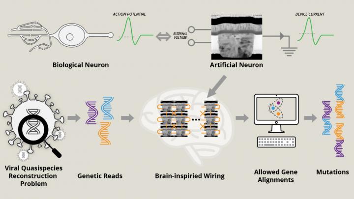
Reminiscent of the plasticity of connections in the human brain, the device can be reconfigured on the fly for different computational tasks by simply changing applied voltages. Furthermore, like nerve cells can store memories, the same device can also retain information for future retrieval and processing.

Two of the universities involved in the research have issued news/press releases. I’m going to start with the September 1, 2021 Texas A&M University news release (also on EurekAlert), which originated the news item on ScienceDaily,

“The brain has the remarkable ability to change its wiring around by making and breaking connections between nerve cells. Achieving something comparable in a physical system has been extremely challenging,” said Dr. R. Stanley Williams [emphasis mine], professor in the Department of Electrical and Computer Engineering at Texas A&M University. “We have now created a molecular device with dramatic reconfigurability, which is achieved not by changing physical connections like in the brain, but by reprogramming its logic.”

Dr. T. Venkatesan, director of the Center for Quantum Research and Technology (CQRT) at the University of Oklahoma, Scientific Affiliate at National Institute of Standards and Technology, Gaithersburg, and adjunct professor of electrical and computer engineering at the National University of Singapore, added that their molecular device might in the future help design next-generation processing chips with enhanced computational power and speed, but consuming significantly reduced energy.

Whether it is the familiar laptop or a sophisticated supercomputer, digital technologies face a common nemesis, the von Neumann bottleneck. This delay in computational processing is a consequence of current computer architectures, wherein the memory, containing data and programs, is physically separated from the processor. As a result, computers spend a significant amount of time shuttling information between the two systems, causing the bottleneck. Also, despite extremely fast processor speeds, these units can be idling for extended amounts of time during periods of information exchange.

As an alternative to conventional electronic parts used for designing memory units and processors, devices called memristors offer a way to circumvent the von Neumann bottleneck. Memristors, such as those made of niobium dioxide and vanadium dioxide, transition from being an insulator to a conductor at a set temperature. This property gives these types of memristors the ability to perform computations and store data.

However, despite their many advantages, these metal oxide memristors are made of rare-earth elements and can operate only in restrictive temperature regimes. Hence, there has been an ongoing search for promising organic molecules that can perform a comparable memristive function, said Williams.

Dr. Sreebrata Goswami, a professor at the Indian Association for the Cultivation of Science, designed the material used in this work. The compound has a central metal atom (iron) bound to three phenyl azo pyridine organic molecules called ligands.

“This behaves like an electron sponge that can absorb as many as six electrons reversibly, resulting in seven different redox states,” said Sreebrata. “The interconnectivity between these states is the key behind the reconfigurability shown in this work.”

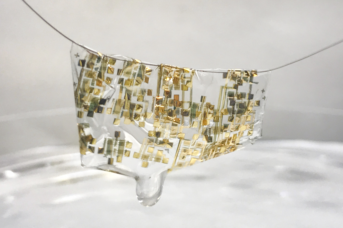
Dr. Sreetosh Goswami, a researcher at the National University of Singapore, devised this project by creating a tiny electrical circuit consisting of a 40-nanometer layer of molecular film sandwiched between a layer of gold on top and gold-infused nanodisc and indium tin oxide at the bottom.

On applying a negative voltage on the device, Sreetosh witnessed a current-voltage profile that was nothing like anyone had seen before. Unlike metal-oxide memristors that can switch from metal to insulator at only one fixed voltage, the organic molecular devices could switch back and forth from insulator to conductor at several discrete sequential voltages.

“So, if you think of the device as an on-off switch, as we were sweeping the voltage more negative, the device first switched from on to off, then off to on, then on to off and then back to on. I’ll say that we were just blown out of our seat,” said Venkatesan. “We had to convince ourselves that what we were seeing was real.”

Sreetosh and Sreebrata investigated the molecular mechanisms underlying the curious switching behavior using an imaging technique called Raman spectroscopy. In particular, they looked for spectral signatures in the vibrational motion of the organic molecule that could explain the multiple transitions. Their investigation revealed that sweeping the voltage negative triggered the ligands on the molecule to undergo a series of reduction, or electron-gaining, events that caused the molecule to transition between off state and on states.

Next, to describe the extremely complex current-voltage profile of the molecular device mathematically, Williams deviated from the conventional approach of basic physics-based equations. Instead, he described the behavior of the molecules using a decision tree algorithm with “if-then-else” statements, a commonplace line of code in several computer programs, particularly digital games.

“Video games have a structure where you have a character that does something, and then something occurs as a result. And so, if you write that out in a computer algorithm, they are if-then-else statements,” said Williams. “Here, the molecule is switching from on to off as a consequence of applied voltage, and that’s when I had the eureka moment to use decision trees to describe these devices, and it worked very well.” 

But the researchers went a step further to exploit these molecular devices to run programs for different real-world computational tasks. Sreetosh showed experimentally that their devices could perform fairly complex computations in a single time step and then be reprogrammed to perform another task in the next instant.

“It was quite extraordinary; our device was doing something like what the brain does, but in a very different way,” said Sreetosh. “When you’re learning something new or when you’re deciding, the brain can actually reconfigure and change physical wiring around. Similarly, we can logically reprogram or reconfigure our devices by giving them a different voltage pulse then they’ve seen before.” 

Venkatesan noted that it would take thousands of transistors to perform the same computational functions as one of their molecular devices with its different decision trees. Hence, he said their technology might first be used in handheld devices, like cell phones and sensors, and other applications where power is limited.

Other contributors to the research include Dr. Abhijeet Patra and Dr. Ariando from the National University of Singapore; Dr. Rajib Pramanick and Dr. Santi Prasad Rath from the Indian Association for the Cultivation of Science; Dr. Martin Foltin from Hewlett Packard Enterprise, Colorado; and Dr. Damien Thompson from the University of Limerick, Ireland.

Venkatesan said that this research is indicative of the future discoveries from this collaborative team, which will include the center of nanoscience and engineering at the Indian Institute of Science and the Microsystems and Nanotechnology Division at the NIST.

I’ve highlighted R. Stanley Williams because he and his team at HP [Hewlett Packard] Labs helped to kick off current memristor research in 2008 with the publication of two papers as per my April 5, 2010 posting,

In 2008, two memristor papers were published in Nature and Nature Nanotechnology, respectively. In the first (Nature, May 2008 [article still behind a paywall], a team at HP Labs claimed they had proved the existence of memristors (a fourth member of electrical engineering’s ‘Holy Trinity of the capacitor, resistor, and inductor’). In the second paper (Nature Nanotechnology, July 2008 [article still behind a paywall]) the team reported that they had achieved engineering control.

The novel memory device is based on a molecular system that can transition between on and off states at several discrete sequential voltages Courtesy: National University of Singapore

There is more technical detail in the September 2, 2022 NUS press release (also on EurekAlert),

Many electronic devices today are dependent on semiconductor logic circuits based on switches hard-wired to perform predefined logic functions. Physicists from the National University of Singapore (NUS), together with an international team of researchers, have developed a novel molecular memristor, or an electronic memory device, that has exceptional memory reconfigurability. 

Unlike hard-wired standard circuits, the molecular device can be reconfigured using voltage to embed different computational tasks. The energy-efficient new technology, which is capable of enhanced computational power and speed, can potentially be used in edge computing, as well as handheld devices and applications with limited power resource.

“This work is a significant breakthrough in our quest to design low-energy computing. The idea of using multiple switching in a single element draws inspiration from how the brain works and fundamentally reimagines the design strategy of a logic circuit,” said Associate Professor Ariando from the NUS Department of Physics who led the research.

The research was first published in the journal Nature on 1 September 2021, and carried out in collaboration with the Indian Association for the Cultivation of Science, Hewlett Packard Enterprise, the University of Limerick, the University of Oklahoma, and Texas A&M University.

Brain-inspired technology

“This new discovery can contribute to developments in edge computing as a sophisticated in-memory computing approach to overcome the von Neumann bottleneck, a delay in computational processing seen in many digital technologies due to the physical separation of memory storage from a device’s processor,” said Assoc Prof Ariando. The new molecular device also has the potential to contribute to designing next generation processing chips with enhanced computational power and speed.

“Similar to the flexibility and adaptability of connections in the human brain, our memory device can be reconfigured on the fly for different computational tasks by simply changing applied voltages. Furthermore, like how nerve cells can store memories, the same device can also retain information for future retrieval and processing,” said first author Dr Sreetosh Goswami, Research Fellow from the Department of Physics at NUS.

Research team member Dr Sreebrata Goswami, who was a Senior Research Scientist at NUS and previously Professor at the Indian Association for the Cultivation of Science, conceptualised and designed a molecular system belonging to the chemical family of phenyl azo pyridines that have a central metal atom bound to organic molecules called ligands. “These molecules are like electron sponges that can offer as many as six electron transfers resulting in five different molecular states. The interconnectivity between these states is the key behind the device’s reconfigurability,” explained Dr Sreebrata Goswami.

Dr Sreetosh Goswami created a tiny electrical circuit consisting a 40-nanometer layer of molecular film sandwiched between a top layer of gold, and a bottom layer of gold-infused nanodisc and indium tin oxide. He observed an unprecedented current-voltage profile upon applying a negative voltage to the device. Unlike conventional metal-oxide memristors that are switched on and off at only one fixed voltage, these organic molecular devices could switch between on-off states at several discrete sequential voltages.

Using an imaging technique called Raman spectroscopy, spectral signatures in the vibrational motion of the organic molecule were observed to explain the multiple transitions. Dr Sreebrata Goswami explained, “Sweeping the negative voltage triggered the ligands on the molecule to undergo a series of reduction, or electron-gaining which caused the molecule to transition between off and on states.”

The researchers described the behavior of the molecules using a decision tree algorithm with “if-then-else” statements, which is used in the coding of several computer programs, particularly digital games, as compared to the conventional approach of using basic physics-based equations.

New possibilities for energy-efficient devices

Building on their research, the team used the molecular memory devices to run programs for different real-world computational tasks. As a proof of concept, the team demonstrated that their technology could perform complex computations in a single step, and could be reprogrammed to perform another task in the next instant. An individual molecular memory device could perform the same computational functions as thousands of transistors, making the technology a more powerful and energy-efficient memory option.

“The technology might first be used in handheld devices, like cell phones and sensors, and other applications where power is limited,” added Assoc Prof Ariando.

The team in the midst of building new electronic devices incorporating their innovation, and working with collaborators to conduct simulation and benchmarking relating to existing technologies.

Other contributors to the research paper include Abhijeet Patra and Santi Prasad Rath from NUS, Rajib Pramanick from the Indian Association for the Cultivation of Science, Martin Foltin from Hewlett Packard Enterprise, Damien Thompson from the University of Limerick, T. Venkatesan from the University of Oklahoma, and R. Stanley Williams from Texas A&M University.

Here’s a link to and a citation for the paper,

Decision trees within a molecular memristor by Sreetosh Goswami, Rajib Pramanick, Abhijeet Patra, Santi Prasad Rath, Martin Foltin, A. Ariando, Damien Thompson, T. Venkatesan, Sreebrata Goswami & R. Stanley Williams. Nature volume 597, pages 51–56 (2021) DOI: https://doi.org/10.1038/s41586-021-03748-0 Published 01 September 2021 Issue Date 02 September 2021

This paper is behind a paywall.

Brain cell-like nanodevices

Given R. Stanley Williams’s presence on the author list, it’s a bit surprising that there’s no mention of memristors. If I read the signs rightly the interest is shifting, in some cases, from the memristor to a more comprehensive grouping of circuit elements referred to as ‘neuristors’ or, more likely, ‘nanocirucuit elements’ in the effort to achieve brainlike (neuromorphic) computing (engineering). (Williams was the leader of the HP Labs team that offered proof and more of the memristor’s existence, which I mentioned here in an April 5, 2010 posting. There are many, many postings on this topic here; try ‘memristors’ or ‘brainlike computing’ for your search terms.)

A September 24, 2020 news item on ScienceDaily announces a recent development in the field of neuromorphic engineering,

In the September [2020] issue of the journal Nature, scientists from Texas A&M University, Hewlett Packard Labs and Stanford University have described a new nanodevice that acts almost identically to a brain cell. Furthermore, they have shown that these synthetic brain cells can be joined together to form intricate networks that can then solve problems in a brain-like manner.

“This is the first study where we have been able to emulate a neuron with just a single nanoscale device, which would otherwise need hundreds of transistors,” said Dr. R. Stanley Williams, senior author on the study and professor in the Department of Electrical and Computer Engineering. “We have also been able to successfully use networks of our artificial neurons to solve toy versions of a real-world problem that is computationally intense even for the most sophisticated digital technologies.”

In particular, the researchers have demonstrated proof of concept that their brain-inspired system can identify possible mutations in a virus, which is highly relevant for ensuring the efficacy of vaccines and medications for strains exhibiting genetic diversity.

A September 24, 2020 Texas A&M University news release (also on EurekAlert) by Vandana Suresh, which originated the news item, provides some context for the research,

Over the past decades, digital technologies have become smaller and faster largely because of the advancements in transistor technology. However, these critical circuit components are fast approaching their limit of how small they can be built, initiating a global effort to find a new type of technology that can supplement, if not replace, transistors.

In addition to this “scaling-down” problem, transistor-based digital technologies have other well-known challenges. For example, they struggle at finding optimal solutions when presented with large sets of data.

“Let’s take a familiar example of finding the shortest route from your office to your home. If you have to make a single stop, it’s a fairly easy problem to solve. But if for some reason you need to make 15 stops in between, you have 43 billion routes to choose from,” said Dr. Suhas Kumar, lead author on the study and researcher at Hewlett Packard Labs. “This is now an optimization problem, and current computers are rather inept at solving it.”

Kumar added that another arduous task for digital machines is pattern recognition, such as identifying a face as the same regardless of viewpoint or recognizing a familiar voice buried within a din of sounds.

But tasks that can send digital machines into a computational tizzy are ones at which the brain excels. In fact, brains are not just quick at recognition and optimization problems, but they also consume far less energy than digital systems. Hence, by mimicking how the brain solves these types of tasks, Williams said brain-inspired or neuromorphic systems could potentially overcome some of the computational hurdles faced by current digital technologies.

To build the fundamental building block of the brain or a neuron, the researchers assembled a synthetic nanoscale device consisting of layers of different inorganic materials, each with a unique function. However, they said the real magic happens in the thin layer made of the compound niobium dioxide.

When a small voltage is applied to this region, its temperature begins to increase. But when the temperature reaches a critical value, niobium dioxide undergoes a quick change in personality, turning from an insulator to a conductor. But as it begins to conduct electric currents, its temperature drops and niobium dioxide switches back to being an insulator.

These back-and-forth transitions enable the synthetic devices to generate a pulse of electrical current that closely resembles the profile of electrical spikes, or action potentials, produced by biological neurons. Further, by changing the voltage across their synthetic neurons, the researchers reproduced a rich range of neuronal behaviors observed in the brain, such as sustained, burst and chaotic firing of electrical spikes.

“Capturing the dynamical behavior of neurons is a key goal for brain-inspired computers,” said Kumar. “Altogether, we were able to recreate around 15 types of neuronal firing profiles, all using a single electrical component and at much lower energies compared to transistor-based circuits.”

To evaluate if their synthetic neurons [neuristor?] can solve real-world problems, the researchers first wired 24 such nanoscale devices together in a network inspired by the connections between the brain’s cortex and thalamus, a well-known neural pathway involved in pattern recognition. Next, they used this system to solve a toy version of the viral quasispecies reconstruction problem, where mutant variations of a virus are identified without a reference genome.

By means of data inputs, the researchers introduced the network to short gene fragments. Then, by programming the strength of connections between the artificial neurons within the network, they established basic rules about joining these genetic fragments. The jigsaw puzzle-like task for the network was to list mutations in the virus’ genome based on these short genetic segments.

The researchers found that within a few microseconds, their network of artificial neurons settled down in a state that was indicative of the genome for a mutant strain.

Williams and Kumar noted this result is proof of principle that their neuromorphic systems can quickly perform tasks in an energy-efficient way.

The researchers said the next steps in their research will be to expand the repertoire of the problems that their brain-like networks can solve by incorporating other firing patterns and some hallmark properties of the human brain like learning and memory. They also plan to address hardware challenges for implementing their technology on a commercial scale.

“Calculating the national debt or solving some large-scale simulation is not the type of task the human brain is good at and that’s why we have digital computers. Alternatively, we can leverage our knowledge of neuronal connections for solving problems that the brain is exceptionally good at,” said Williams. “We have demonstrated that depending on the type of problem, there are different and more efficient ways of doing computations other than the conventional methods using digital computers with transistors.”

If you look at the news release on EurekAlert, you’ll see this informative image is titled: NeuristerSchematic [sic],

Caption: Networks of artificial neurons connected together can solve toy versions the viral quasispecies reconstruction problem. Credit: Texas A&M University College of Engineering

(On the university website, the image is credited to Rachel Barton.) You can see one of the first mentions of a ‘neuristor’ here in an August 24, 2017 posting.

Here’s a link to and a citation for the paper,

Third-order nanocircuit elements for neuromorphic engineering by Suhas Kumar, R. Stanley Williams & Ziwen Wang. Nature volume 585, pages518–523(2020) DOI: https://doi.org/10.1038/s41586-020-2735-5 Published: 23 September 2020 Issue Date: 24 September 2020

This paper is behind a paywall.

Mott memristor

Mott memristors (mentioned in my Aug. 24, 2017 posting about neuristors and brainlike computing) gets more fulsome treatment in an Oct. 9, 2017 posting by Samuel K. Moore on the Nanoclast blog (found on the IEEE [Institute of Electrical and Electronics Engineers] website) Note: 1: Links have been removed; Note 2 : I quite like Moore’s writing style but he’s not for the impatient reader,

When you’re really harried, you probably feel like your head is brimful of chaos. You’re pretty close. Neuroscientists say your brain operates in a regime termed the “edge of chaos,” and it’s actually a good thing. It’s a state that allows for fast, efficient analog computation of the kind that can solve problems that grow vastly more difficult as they become bigger in size.

The trouble is, if you’re trying to replicate that kind of chaotic computation with electronics, you need an element that both acts chaotically—how and when you want it to—and could scale up to form a big system.

“No one had been able to show chaotic dynamics in a single scalable electronic device,” says Suhas Kumar, a researcher at Hewlett Packard Labs, in Palo Alto, Calif. Until now, that is.

He, John Paul Strachan, and R. Stanley Williams recently reported in the journal Nature that a particular configuration of a certain type of memristor contains that seed of controlled chaos. What’s more, when they simulated wiring these up into a type of circuit called a Hopfield neural network, the circuit was capable of solving a ridiculously difficult problem—1,000 instances of the traveling salesman problem—at a rate of 10 trillion operations per second per watt.

(It’s not an apples-to-apples comparison, but the world’s most powerful supercomputer as of June 2017 managed 93,015 trillion floating point operations per second but consumed 15 megawatts doing it. So about 6 billion operations per second per watt.)

The device in question is called a Mott memristor. Memristors generally are devices that hold a memory, in the form of resistance, of the current that has flowed through them. The most familiar type is called resistive RAM (or ReRAM or RRAM, depending on who’s asking). Mott memristors have an added ability in that they can also reflect a temperature-driven change in resistance.

The HP Labs team made their memristor from an 8-nanometer-thick layer of niobium dioxide (NbO2) sandwiched between two layers of titanium nitride. The bottom titanium nitride layer was in the form of a 70-nanometer wide pillar. “We showed that this type of memristor can generate chaotic and nonchaotic signals,” says Williams, who invented the memristor based on theory by Leon Chua.

(The traveling salesman problem is one of these. In it, the salesman must find the shortest route that lets him visit all of his customers’ cities, without going through any of them twice. It’s a difficult problem because it becomes exponentially more difficult to solve with each city you add.)

Here’s what the niobium dioxide-based Mott memristor looks like,

Photo: Suhas Kumar/Hewlett Packard Labs
A micrograph shows the construction of a Mott memristor composed of an 8-nanometer-thick layer of niobium dioxide between two layers of titanium nitride.

Here’s a link to and a citation for the paper,

Chaotic dynamics in nanoscale NbO2 Mott memristors for analogue computing by Suhas Kumar, John Paul Strachan & R. Stanley Williams. Nature 548, 318–321 (17 August 2017) doi:10.1038/nature23307 Published online: 09 August 2017

This paper is behind a paywall.

Gamechanging electronics with new ultrafast, flexible, and transparent electronics

There are two news bits about game-changing electronics, one from the UK and the other from the US.

United Kingdom (UK)

An April 3, 2017 news item on Azonano announces the possibility of a future golden age of electronics courtesy of the University of Exeter,

Engineering experts from the University of Exeter have come up with a breakthrough way to create the smallest, quickest, highest-capacity memories for transparent and flexible applications that could lead to a future golden age of electronics.

A March 31, 2017 University of Exeter press release (also on EurekAlert), which originated the news item, expands on the theme (Note: Links have been removed),

Engineering experts from the University of Exeter have developed innovative new memory using a hybrid of graphene oxide and titanium oxide. Their devices are low cost and eco-friendly to produce, are also perfectly suited for use in flexible electronic devices such as ‘bendable’ mobile phone, computer and television screens, and even ‘intelligent’ clothing.

Crucially, these devices may also have the potential to offer a cheaper and more adaptable alternative to ‘flash memory’, which is currently used in many common devices such as memory cards, graphics cards and USB computer drives.

The research team insist that these innovative new devices have the potential to revolutionise not only how data is stored, but also take flexible electronics to a new age in terms of speed, efficiency and power.

Professor David Wright, an Electronic Engineering expert from the University of Exeter and lead author of the paper said: “Using graphene oxide to produce memory devices has been reported before, but they were typically very large, slow, and aimed at the ‘cheap and cheerful’ end of the electronics goods market.

“Our hybrid graphene oxide-titanium oxide memory is, in contrast, just 50 nanometres long and 8 nanometres thick and can be written to and read from in less than five nanoseconds – with one nanometre being one billionth of a metre and one nanosecond a billionth of a second.”

Professor Craciun, a co-author of the work, added: “Being able to improve data storage is the backbone of tomorrow’s knowledge economy, as well as industry on a global scale. Our work offers the opportunity to completely transform graphene-oxide memory technology, and the potential and possibilities it offers.”

Here’s a link to and a citation for the paper,

Multilevel Ultrafast Flexible Nanoscale Nonvolatile Hybrid Graphene Oxide–Titanium Oxide Memories by V. Karthik Nagareddy, Matthew D. Barnes, Federico Zipoli, Khue T. Lai, Arseny M. Alexeev, Monica Felicia Craciun, and C. David Wright. ACS Nano, 2017, 11 (3), pp 3010–3021 DOI: 10.1021/acsnano.6b08668 Publication Date (Web): February 21, 2017

Copyright © 2017 American Chemical Society

This paper appears to be open access.

United States (US)

Researchers from Stanford University have developed flexible, biodegradable electronics.

A newly developed flexible, biodegradable semiconductor developed by Stanford engineers shown on a human hair. (Image credit: Bao lab)

A human hair? That’s amazing and this May 3, 2017 news item on Nanowerk reveals more,

As electronics become increasingly pervasive in our lives – from smart phones to wearable sensors – so too does the ever rising amount of electronic waste they create. A United Nations Environment Program report found that almost 50 million tons of electronic waste were thrown out in 2017–more than 20 percent higher than waste in 2015.

Troubled by this mounting waste, Stanford engineer Zhenan Bao and her team are rethinking electronics. “In my group, we have been trying to mimic the function of human skin to think about how to develop future electronic devices,” Bao said. She described how skin is stretchable, self-healable and also biodegradable – an attractive list of characteristics for electronics. “We have achieved the first two [flexible and self-healing], so the biodegradability was something we wanted to tackle.”

The team created a flexible electronic device that can easily degrade just by adding a weak acid like vinegar. The results were published in the Proceedings of the National Academy of Sciences (“Biocompatible and totally disintegrable semiconducting polymer for ultrathin and ultralightweight transient electronics”).

“This is the first example of a semiconductive polymer that can decompose,” said lead author Ting Lei, a postdoctoral fellow working with Bao.

A May 1, 2017 Stanford University news release by Sarah Derouin, which originated the news item, provides more detail,

In addition to the polymer – essentially a flexible, conductive plastic – the team developed a degradable electronic circuit and a new biodegradable substrate material for mounting the electrical components. This substrate supports the electrical components, flexing and molding to rough and smooth surfaces alike. When the electronic device is no longer needed, the whole thing can biodegrade into nontoxic components.

Biodegradable bits

Bao, a professor of chemical engineering and materials science and engineering, had previously created a stretchable electrode modeled on human skin. That material could bend and twist in a way that could allow it to interface with the skin or brain, but it couldn’t degrade. That limited its application for implantable devices and – important to Bao – contributed to waste.

Flexible, biodegradable semiconductor on an avacado

The flexible semiconductor can adhere to smooth or rough surfaces and biodegrade to nontoxic products. (Image credit: Bao lab)

Bao said that creating a robust material that is both a good electrical conductor and biodegradable was a challenge, considering traditional polymer chemistry. “We have been trying to think how we can achieve both great electronic property but also have the biodegradability,” Bao said.

Eventually, the team found that by tweaking the chemical structure of the flexible material it would break apart under mild stressors. “We came up with an idea of making these molecules using a special type of chemical linkage that can retain the ability for the electron to smoothly transport along the molecule,” Bao said. “But also this chemical bond is sensitive to weak acid – even weaker than pure vinegar.” The result was a material that could carry an electronic signal but break down without requiring extreme measures.

In addition to the biodegradable polymer, the team developed a new type of electrical component and a substrate material that attaches to the entire electronic component. Electronic components are usually made of gold. But for this device, the researchers crafted components from iron. Bao noted that iron is a very environmentally friendly product and is nontoxic to humans.

The researchers created the substrate, which carries the electronic circuit and the polymer, from cellulose. Cellulose is the same substance that makes up paper. But unlike paper, the team altered cellulose fibers so the “paper” is transparent and flexible, while still breaking down easily. The thin film substrate allows the electronics to be worn on the skin or even implanted inside the body.

From implants to plants

The combination of a biodegradable conductive polymer and substrate makes the electronic device useful in a plethora of settings – from wearable electronics to large-scale environmental surveys with sensor dusts.

“We envision these soft patches that are very thin and conformable to the skin that can measure blood pressure, glucose value, sweat content,” Bao said. A person could wear a specifically designed patch for a day or week, then download the data. According to Bao, this short-term use of disposable electronics seems a perfect fit for a degradable, flexible design.

And it’s not just for skin surveys: the biodegradable substrate, polymers and iron electrodes make the entire component compatible with insertion into the human body. The polymer breaks down to product concentrations much lower than the published acceptable levels found in drinking water. Although the polymer was found to be biocompatible, Bao said that more studies would need to be done before implants are a regular occurrence.

Biodegradable electronics have the potential to go far beyond collecting heart disease and glucose data. These components could be used in places where surveys cover large areas in remote locations. Lei described a research scenario where biodegradable electronics are dropped by airplane over a forest to survey the landscape. “It’s a very large area and very hard for people to spread the sensors,” he said. “Also, if you spread the sensors, it’s very hard to gather them back. You don’t want to contaminate the environment so we need something that can be decomposed.” Instead of plastic littering the forest floor, the sensors would biodegrade away.

As the number of electronics increase, biodegradability will become more important. Lei is excited by their advancements and wants to keep improving performance of biodegradable electronics. “We currently have computers and cell phones and we generate millions and billions of cell phones, and it’s hard to decompose,” he said. “We hope we can develop some materials that can be decomposed so there is less waste.”

Other authors on the study include Ming Guan, Jia Liu, Hung-Cheng Lin, Raphael Pfattner, Leo Shaw, Allister McGuire, and Jeffrey Tok of Stanford University; Tsung-Ching Huang of Hewlett Packard Enterprise; and Lei-Lai Shao and Kwang-Ting Cheng of University of California, Santa Barbara.

The research was funded by the Air Force Office for Scientific Research; BASF; Marie Curie Cofund; Beatriu de Pinós fellowship; and the Kodak Graduate Fellowship.

Here’s a link to and a citation for the team’s latest paper,

Biocompatible and totally disintegrable semiconducting polymer for ultrathin and ultralightweight transient electronics by Ting Lei, Ming Guan, Jia Liu, Hung-Cheng Lin, Raphael Pfattner, Leo Shaw, Allister F. McGuire, Tsung-Ching Huang, Leilai Shao, Kwang-Ting Cheng, Jeffrey B.-H. Tok, and Zhenan Bao. PNAS 2017 doi: 10.1073/pnas.1701478114 published ahead of print May 1, 2017

This paper is behind a paywall.

The mention of cellulose in the second item piqued my interest so I checked to see if they’d used nanocellulose. No, they did not. Microcrystalline cellulose powder was used to constitute a cellulose film but they found a way to render this film at the nanoscale. From the Stanford paper (Note: Links have been removed),

… Moreover, cellulose films have been previously used as biodegradable substrates in electronics (28⇓–30). However, these cellulose films are typically made with thicknesses well over 10 μm and thus cannot be used to fabricate ultrathin electronics with substrate thicknesses below 1–2 μm (7, 18, 19). To the best of our knowledge, there have been no reports on ultrathin (1–2 μm) biodegradable substrates for electronics. Thus, to realize them, we subsequently developed a method described herein to obtain ultrathin (800 nm) cellulose films (Fig. 1B and SI Appendix, Fig. S8). First, microcrystalline cellulose powders were dissolved in LiCl/N,N-dimethylacetamide (DMAc) and reacted with hexamethyldisilazane (HMDS) (31, 32), providing trimethylsilyl-functionalized cellulose (TMSC) (Fig. 1B). To fabricate films or devices, TMSC in chlorobenzene (CB) (70 mg/mL) was spin-coated on a thin dextran sacrificial layer. The TMSC film was measured to be 1.2 μm. After hydrolyzing the film in 95% acetic acid vapor for 2 h, the trimethylsilyl groups were removed, giving a 400-nm-thick cellulose film. The film thickness significantly decreased to one-third of the original film thickness, largely due to the removal of the bulky trimethylsilyl groups. The hydrolyzed cellulose film is insoluble in most organic solvents, for example, toluene, THF, chloroform, CB, and water. Thus, we can sequentially repeat the above steps to obtain an 800-nm-thick film, which is robust enough for further device fabrication and peel-off. By soaking the device in water, the dextran layer is dissolved, starting from the edges of the device to the center. This process ultimately releases the ultrathin substrate and leaves it floating on water surface (Fig. 3A, Inset).

Finally, I don’t have any grand thoughts; it’s just interesting to see different approaches to flexible electronics.

X-rays reveal memristor workings

A June 14, 2016 news item on ScienceDaily focuses on memristors. (It’s been about two months since my last memristor posting on April 22, 2016 regarding electronic synapses and neural networks). This piece announces new insight into how memristors function at the atomic scale,

In experiments at two Department of Energy national labs — SLAC National Accelerator Laboratory and Lawrence Berkeley National Laboratory — scientists at Hewlett Packard Enterprise (HPE) [also referred to as HP Labs or Hewlett Packard Laboratories] have experimentally confirmed critical aspects of how a new type of microelectronic device, the memristor, works at an atomic scale.

This result is an important step in designing these solid-state devices for use in future computer memories that operate much faster, last longer and use less energy than today’s flash memory. …

“We need information like this to be able to design memristors that will succeed commercially,” said Suhas Kumar, an HPE scientist and first author on the group’s technical paper.

A June 13, 2016 SLAC news release, which originated the news item, offers a brief history according to HPE and provides details about the latest work,

The memristor was proposed theoretically [by Dr. Leon Chua] in 1971 as the fourth basic electrical device element alongside the resistor, capacitor and inductor. At its heart is a tiny piece of a transition metal oxide sandwiched between two electrodes. Applying a positive or negative voltage pulse dramatically increases or decreases the memristor’s electrical resistance. This behavior makes it suitable for use as a “non-volatile” computer memory that, like flash memory, can retain its state without being refreshed with additional power.

Over the past decade, an HPE group led by senior fellow R. Stanley Williams has explored memristor designs, materials and behavior in detail. Since 2009 they have used intense synchrotron X-rays to reveal the movements of atoms in memristors during switching. Despite advances in understanding the nature of this switching, critical details that would be important in designing commercially successful circuits  remained controversial. For example, the forces that move the atoms, resulting in dramatic resistance changes during switching, remain under debate.

In recent years, the group examined memristors made with oxides of titanium, tantalum and vanadium. Initial experiments revealed that switching in the tantalum oxide devices could be controlled most easily, so it was chosen for further exploration at two DOE Office of Science User Facilities – SLAC’s Stanford Synchrotron Radiation Lightsource (SSRL) and Berkeley Lab’s Advanced Light Source (ALS).

At ALS, the HPE researchers mapped the positions of oxygen atoms before and after switching. For this, they used a scanning transmission X-ray microscope and an apparatus they built to precisely control the position of their sample and the timing and intensity of the 500-electronvolt ALS X-rays, which were tuned to see oxygen.

The experiments revealed that even weak voltage pulses create a thin conductive path through the memristor. During the pulse the path heats up, which creates a force that pushes oxygen atoms away from the path, making it even more conductive. Reversing the voltage pulse resets the memristor by sucking some of oxygen atoms back into the conducting path, thereby increasing the device’s resistance. The memristor’s resistance changes between 10-fold and 1 million-fold, depending on operating parameters like the voltage-pulse amplitude. This resistance change is dramatic enough to exploit commercially.

To be sure of their conclusion, the researchers also needed to understand if the tantalum atoms were moving along with the oxygen during switching. Imaging tantalum required higher-energy, 10,000-electronvolt X-rays, which they obtained at SSRL’s Beam Line 6-2. In a single session there, they determined that the tantalum remained stationary.

“That sealed the deal, convincing us that our hypothesis was correct,” said HPE scientist Catherine Graves, who had worked at SSRL as a Stanford graduate student. She added that discussions with SLAC experts were critical in guiding the HPE team toward the X-ray techniques that would allow them to see the tantalum accurately.

Kumar said the most promising aspect of the tantalum oxide results was that the scientists saw no degradation in switching over more than a billion voltage pulses of a magnitude suitable for commercial use. He added that this knowledge helped his group build memristors that lasted nearly a billion switching cycles, about a thousand-fold improvement.

“This is much longer endurance than is possible with today’s flash memory devices,” Kumar said. “In addition, we also used much higher voltage pulses to accelerate and observe memristor failures, which is also important in understanding how these devices work. Failures occurred when oxygen atoms were forced so far away that they did not return to their initial positions.”

Beyond memory chips, Kumar says memristors’ rapid switching speed and small size could make them suitable for use in logic circuits. Additional memristor characteristics may also be beneficial in the emerging class of brain-inspired neuromorphic computing circuits.

“Transistors are big and bulky compared to memristors,” he said. “Memristors are also much better suited for creating the neuron-like voltage spikes that characterize neuromorphic circuits.”

The researchers have provided an animation illustrating how memristors can fail,

This animation shows how millions of high-voltage switching cycles can cause memristors to fail. The high-voltage switching eventually creates regions that are permanently rich (blue pits) or deficient (red peaks) in oxygen and cannot be switched back. Switching at lower voltages that would be suitable for commercial devices did not show this performance degradation. These observations allowed the researchers to develop materials processing and operating conditions that improved the memristors’ endurance by nearly a thousand times. (Suhas Kumar) Courtesy: SLAC

This animation shows how millions of high-voltage switching cycles can cause memristors to fail. The high-voltage switching eventually creates regions that are permanently rich (blue pits) or deficient (red peaks) in oxygen and cannot be switched back. Switching at lower voltages that would be suitable for commercial devices did not show this performance degradation. These observations allowed the researchers to develop materials processing and operating conditions that improved the memristors’ endurance by nearly a thousand times. (Suhas Kumar) Courtesy: SLAC

Here’s a link to and a citation for the paper,

Direct Observation of Localized Radial Oxygen Migration in Functioning Tantalum Oxide Memristors by Suhas Kumar, Catherine E. Graves, John Paul Strachan, Emmanuelle Merced Grafals, Arthur L. David Kilcoyne3, Tolek Tyliszczak, Johanna Nelson Weker, Yoshio Nishi, and R. Stanley Williams. Advanced Materials, First published: 2 February 2016; Print: Volume 28, Issue 14 April 13, 2016 Pages 2772–2776 DOI: 10.1002/adma.201505435

This paper is behind a paywall.

Some of the ‘memristor story’ is contested and you can find a brief overview of the discussion in this Wikipedia memristor entry in the section on ‘definition and criticism’. There is also a history of the memristor which dates back to the 19th century featured in my May 22, 2012 posting.

A perovskite memristor with three stable resistive states

Thanks to Dexter Johnson’s Oct. 22, 2015 posting on his Nanoclast blog (on the IEEE [Institute of Electrical and Electronics Engineers]) website, I’ve found information about a second memristor with three terminals, aka, three stable resistive states,  (the first is mentioned in my April 10, 2015 posting). From Dexter’s posting (Note: Links have been removed),

Now researchers at ETH Zurich have designed a memristor device out of perovskite just 5 nanometres thick that has three stable resistive states, which means it can encode data as 0,1 and 2, or a “trit” as opposed to a “bit.”

The research, which was published in the journal ACS Nano, developed model devices that have two competing nonvolatile resistive switching processes. These switching processes can be alternatively triggered by the effective switching voltage and time applied to the device.

“Our component could therefore also be useful for a new type of IT (Information Technology) that is not based on binary logic, but on a logic that provides for information located ‘between’ the 0 and 1,” said Jennifer Rupp, professor in the Department of Materials at ETH Zurich, in a press release. “This has interesting implications for what is referred to as fuzzy logic, which seeks to incorporate a form of uncertainty into the processing of digital information. You could describe it as less rigid computing.”

An Oct. 19, 2015 Swiss National Science Foundation press release provides context for the research,

Two IT giants, Intel and HP, have entered a race to produce a commercial version of memristors, a new electronics component that could one day replace flash memory (DRAM) used in USB memory sticks, SD cards and SSD hard drives. “Basically, memristors require less energy since they work at lower voltages,” explains Jennifer Rupp, professor in the Department of Materials at ETH Zurich and holder of a SNSF professorship grant. “They can be made much smaller than today’s memory modules, and therefore offer much greater density. This means they can store more megabytes of information per square millimetre.” But currently memristors are only at the prototype stage. [emphasis mine]

There is a memristor-based product on the market as I noted in a Sept. 10, 2015 posting, although that may not be the type of memristive device that Rupp seems to be discussing. (Should you have problems accessing the Swiss National Science Foundation press release, you can find a lightly edited version (a brief [two sentences] history of the memristor has been left out) here on Azonano.

Jacopo Prisco wrote for CNN online in a March 2, 2015 article about memristors and Rupp’s work (Note: A link has been removed),

Simply put, the memristor could mean the end of electronics as we know it and the beginning of a new era called “ionics”.

The transistor, developed in 1947, is the main component of computer chips. It functions using a flow of electrons, whereas the memristor couples the electrons with ions, or electrically charged atoms.

In a transistor, once the flow of electrons is interrupted by, say, cutting the power, all information is lost. But a memristor can remember the amount of charge that was flowing through it, and much like a memory stick it will retain the data even when the power is turned off.

This can pave the way for computers that will instantly turn on and off like a light bulb and never lose data: the RAM, or memory, will no longer be erased when the machine is turned off, without the need to save anything to hard drives as with current technology.

Jennifer Rupp is a Professor of electrochemical materials at ETH Zurich, and she’s working with IBM to build a memristor-based machine.

Memristors, she points out, function in a way that is similar to a human brain: “Unlike a transistor, which is based on binary codes, a memristor can have multi-levels. You could have several states, let’s say zero, one half, one quarter, one third, and so on, and that gives us a very powerful new perspective on how our computers may develop in the future,” she told CNN’s Nick Glass.

This is the CNN interview with Rupp,

Prisco also provides an update about HP’s memristor-based product,

After manufacturing the first ever memristor, Hewlett Packard has been working for years on a new type of computer based on the technology. According to plans, it will launch by 2020.

Simply called “The Machine”, it uses “electrons for processing, photons for communication, and ions for storage.”

I first wrote about HP’s The Machine in a June 25, 2014 posting (scroll down about 40% of the way).

There are many academic teams researching memristors including a team at Northwestern University. I highlighted their announcement of a three-terminal version in an April 10, 2015 posting. While Rupp’s team achieved its effect with a perovskite substrate, the Northwestern team used a molybdenum disulfide (MoS2) substrate.

For anyone wanting to read the latest research from ETH, here’s a link to and a citation for the paper,

Uncovering Two Competing Switching Mechanisms for Epitaxial and Ultrathin Strontium Titanate-Based Resistive Switching Bits by Markus Kubicek, Rafael Schmitt, Felix Messerschmitt, and Jennifer L. M. Rupp. ACS Nano, Article ASAP DOI: 10.1021/acsnano.5b02752 Publication Date (Web): October 8, 2015

Copyright © 2015 American Chemical Society

This paper is behind a paywall.

Finally, should you find the commercialization aspects of the memristor story interesting, there’s a June 6, 2015 posting by Knowm CEO (chief executive officer) Alex Nugent waxes eloquent on HP Labs’ ‘memristor problem’ (Note: A link has been removed),

Today I read something that did not surprise me. HP has said that their memristor technology will be replaced by traditional DRAM memory for use in “The Machine”. This is not surprising for those of us who have been in the field since before HP’s memristor marketing engine first revved up in 2008. While I have to admit the miscommunication between HP’s research and business development departments is starting to get really old, I do understand the problem, or at least part of it.

There are two ways to develop memristors. The first way is to force them to behave as you want them to behave. Most memristors that I have seen do not behave like fast, binary, non-volatile, deterministic switches. This is a problem because this is how HP wants them to behave. Consequently a perception has been created that memristors are for non-volatile fast memory. HP wants a drop-in replacement for standard memory because this is a large and established market. Makes sense of course, but its not the whole story on memristors.

Memristors exhibit a huge range of amazing phenomena. Some are very fast to switch but operate probabilistically. Others can be changed a little bit at a time and are ideal for learning. Still others have capacitance (with memory), or act as batteries. I’ve even seen some devices that can be programmed to be a capacitor or a resistor or a memristor. (Seriously).

Nugent, whether you agree with him or not provides, some fascinating insight. In the excerpt I’ve included here, he seems to provide confirmation that it’s possible to state ‘there are no memristors on the market’ and ‘there are memristors on the market’ because different devices are being called memristors.

IBM weighs in with plans for a 7nm computer chip

On the heels of Intel’s announcement about a deal utilizing their 14nm low-power manufacturing process and speculations about a 10nm computer chip (my July 9, 2014 posting), IBM makes an announcement about a 7nm chip as per this July 10, 2014 news item on Azonano,

IBM today [July 10, 2014] announced it is investing $3 billion over the next 5 years in two broad research and early stage development programs to push the limits of chip technology needed to meet the emerging demands of cloud computing and Big Data systems. These investments will push IBM’s semiconductor innovations from today’s breakthroughs into the advanced technology leadership required for the future.

A very comprehensive July 10, 2014 news release lays out the company’s plans for this $3B investment representing 10% of IBM’s total research budget,

The first research program is aimed at so-called “7 nanometer and beyond” silicon technology that will address serious physical challenges that are threatening current semiconductor scaling techniques and will impede the ability to manufacture such chips. The second is focused on developing alternative technologies for post-silicon era chips using entirely different approaches, which IBM scientists and other experts say are required because of the physical limitations of silicon based semiconductors.

Cloud and big data applications are placing new challenges on systems, just as the underlying chip technology is facing numerous significant physical scaling limits.  Bandwidth to memory, high speed communication and device power consumption are becoming increasingly challenging and critical.

The teams will comprise IBM Research scientists and engineers from Albany and Yorktown, New York; Almaden, California; and Europe. In particular, IBM will be investing significantly in emerging areas of research that are already underway at IBM such as carbon nanoelectronics, silicon photonics, new memory technologies, and architectures that support quantum and cognitive computing. [emphasis mine]

These teams will focus on providing orders of magnitude improvement in system level performance and energy efficient computing. In addition, IBM will continue to invest in the nanosciences and quantum computing–two areas of fundamental science where IBM has remained a pioneer for over three decades.

7 nanometer technology and beyond

IBM Researchers and other semiconductor experts predict that while challenging, semiconductors show promise to scale from today’s 22 nanometers down to 14 and then 10 nanometers in the next several years.  However, scaling to 7 nanometers and perhaps below, by the end of the decade will require significant investment and innovation in semiconductor architectures as well as invention of new tools and techniques for manufacturing.

“The question is not if we will introduce 7 nanometer technology into manufacturing, but rather how, when, and at what cost?” said John Kelly, senior vice president, IBM Research. “IBM engineers and scientists, along with our partners, are well suited for this challenge and are already working on the materials science and device engineering required to meet the demands of the emerging system requirements for cloud, big data, and cognitive systems. This new investment will ensure that we produce the necessary innovations to meet these challenges.”

“Scaling to 7nm and below is a terrific challenge, calling for deep physics competencies in processing nano materials affinities and characteristics. IBM is one of a very few companies who has repeatedly demonstrated this level of science and engineering expertise,” said Richard Doherty, technology research director, The Envisioneering Group.

Bridge to a “Post-Silicon” Era

Silicon transistors, tiny switches that carry information on a chip, have been made smaller year after year, but they are approaching a point of physical limitation. Their increasingly small dimensions, now reaching the nanoscale, will prohibit any gains in performance due to the nature of silicon and the laws of physics. Within a few more generations, classical scaling and shrinkage will no longer yield the sizable benefits of lower power, lower cost and higher speed processors that the industry has become accustomed to.

With virtually all electronic equipment today built on complementary metal–oxide–semiconductor (CMOS) technology, there is an urgent need for new materials and circuit architecture designs compatible with this engineering process as the technology industry nears physical scalability limits of the silicon transistor.

Beyond 7 nanometers, the challenges dramatically increase, requiring a new kind of material to power systems of the future, and new computing platforms to solve problems that are unsolvable or difficult to solve today. Potential alternatives include new materials such as carbon nanotubes, and non-traditional computational approaches such as neuromorphic computing, cognitive computing, machine learning techniques, and the science behind quantum computing.

As the leader in advanced schemes that point beyond traditional silicon-based computing, IBM holds over 500 patents for technologies that will drive advancements at 7nm and beyond silicon — more than twice the nearest competitor. These continued investments will accelerate the invention and introduction into product development for IBM’s highly differentiated computing systems for cloud, and big data analytics.

Several exploratory research breakthroughs that could lead to major advancements in delivering dramatically smaller, faster and more powerful computer chips, include quantum computing, neurosynaptic computing, silicon photonics, carbon nanotubes, III-V technologies, low power transistors and graphene:

Quantum Computing

The most basic piece of information that a typical computer understands is a bit. Much like a light that can be switched on or off, a bit can have only one of two values: “1” or “0.” Described as superposition, this special property of qubits enables quantum computers to weed through millions of solutions all at once, while desktop PCs would have to consider them one at a time.

IBM is a world leader in superconducting qubit-based quantum computing science and is a pioneer in the field of experimental and theoretical quantum information, fields that are still in the category of fundamental science – but one that, in the long term, may allow the solution of problems that are today either impossible or impractical to solve using conventional machines. The team recently demonstrated the first experimental realization of parity check with three superconducting qubits, an essential building block for one type of quantum computer.

Neurosynaptic Computing

Bringing together nanoscience, neuroscience, and supercomputing, IBM and university partners have developed an end-to-end ecosystem including a novel non-von Neumann architecture, a new programming language, as well as applications. This novel technology allows for computing systems that emulate the brain’s computing efficiency, size and power usage. IBM’s long-term goal is to build a neurosynaptic system with ten billion neurons and a hundred trillion synapses, all while consuming only one kilowatt of power and occupying less than two liters of volume.

Silicon Photonics

IBM has been a pioneer in the area of CMOS integrated silicon photonics for over 12 years, a technology that integrates functions for optical communications on a silicon chip, and the IBM team has recently designed and fabricated the world’s first monolithic silicon photonics based transceiver with wavelength division multiplexing.  Such transceivers will use light to transmit data between different components in a computing system at high data rates, low cost, and in an energetically efficient manner.

Silicon nanophotonics takes advantage of pulses of light for communication rather than traditional copper wiring and provides a super highway for large volumes of data to move at rapid speeds between computer chips in servers, large datacenters, and supercomputers, thus alleviating the limitations of congested data traffic and high-cost traditional interconnects.

Businesses are entering a new era of computing that requires systems to process and analyze, in real-time, huge volumes of information known as Big Data. Silicon nanophotonics technology provides answers to Big Data challenges by seamlessly connecting various parts of large systems, whether few centimeters or few kilometers apart from each other, and move terabytes of data via pulses of light through optical fibers.

III-V technologies

IBM researchers have demonstrated the world’s highest transconductance on a self-aligned III-V channel metal-oxide semiconductor (MOS) field-effect transistors (FETs) device structure that is compatible with CMOS scaling. These materials and structural innovation are expected to pave path for technology scaling at 7nm and beyond.  With more than an order of magnitude higher electron mobility than silicon, integrating III-V materials into CMOS enables higher performance at lower power density, allowing for an extension to power/performance scaling to meet the demands of cloud computing and big data systems.

Carbon Nanotubes

IBM Researchers are working in the area of carbon nanotube (CNT) electronics and exploring whether CNTs can replace silicon beyond the 7 nm node.  As part of its activities for developing carbon nanotube based CMOS VLSI circuits, IBM recently demonstrated — for the first time in the world — 2-way CMOS NAND gates using 50 nm gate length carbon nanotube transistors.

IBM also has demonstrated the capability for purifying carbon nanotubes to 99.99 percent, the highest (verified) purities demonstrated to date, and transistors at 10 nm channel length that show no degradation due to scaling–this is unmatched by any other material system to date.

Carbon nanotubes are single atomic sheets of carbon rolled up into a tube. The carbon nanotubes form the core of a transistor device that will work in a fashion similar to the current silicon transistor, but will be better performing. They could be used to replace the transistors in chips that power data-crunching servers, high performing computers and ultra fast smart phones.

Carbon nanotube transistors can operate as excellent switches at molecular dimensions of less than ten nanometers – the equivalent to 10,000 times thinner than a strand of human hair and less than half the size of the leading silicon technology. Comprehensive modeling of the electronic circuits suggests that about a five to ten times improvement in performance compared to silicon circuits is possible.

Graphene

Graphene is pure carbon in the form of a one atomic layer thick sheet.  It is an excellent conductor of heat and electricity, and it is also remarkably strong and flexible.  Electrons can move in graphene about ten times faster than in commonly used semiconductor materials such as silicon and silicon germanium. Its characteristics offer the possibility to build faster switching transistors than are possible with conventional semiconductors, particularly for applications in the handheld wireless communications business where it will be a more efficient switch than those currently used.

Recently in 2013, IBM demonstrated the world’s first graphene based integrated circuit receiver front end for wireless communications. The circuit consisted of a 2-stage amplifier and a down converter operating at 4.3 GHz.

Next Generation Low Power Transistors

In addition to new materials like CNTs, new architectures and innovative device concepts are required to boost future system performance. Power dissipation is a fundamental challenge for nanoelectronic circuits. To explain the challenge, consider a leaky water faucet — even after closing the valve as far as possible water continues to drip — this is similar to today’s transistor, in that energy is constantly “leaking” or being lost or wasted in the off-state.

A potential alternative to today’s power hungry silicon field effect transistors are so-called steep slope devices. They could operate at much lower voltage and thus dissipate significantly less power. IBM scientists are researching tunnel field effect transistors (TFETs). In this special type of transistors the quantum-mechanical effect of band-to-band tunneling is used to drive the current flow through the transistor. TFETs could achieve a 100-fold power reduction over complementary CMOS transistors, so integrating TFETs with CMOS technology could improve low-power integrated circuits.

Recently, IBM has developed a novel method to integrate III-V nanowires and heterostructures directly on standard silicon substrates and built the first ever InAs/Si tunnel diodes and TFETs using InAs as source and Si as channel with wrap-around gate as steep slope device for low power consumption applications.

“In the next ten years computing hardware systems will be fundamentally different as our scientists and engineers push the limits of semiconductor innovations to explore the post-silicon future,” said Tom Rosamilia, senior vice president, IBM Systems and Technology Group. “IBM Research and Development teams are creating breakthrough innovations that will fuel the next era of computing systems.”

IBM’s historic contributions to silicon and semiconductor innovation include the invention and/or first implementation of: the single cell DRAM, the “Dennard scaling laws” underpinning “Moore’s Law”, chemically amplified photoresists, copper interconnect wiring, Silicon on Insulator, strained engineering, multi core microprocessors, immersion lithography, high speed silicon germanium (SiGe), High-k gate dielectrics, embedded DRAM, 3D chip stacking, and Air gap insulators.

IBM researchers also are credited with initiating the era of nano devices following the Nobel prize winning invention of the scanning tunneling microscope which enabled nano and atomic scale invention and innovation.

IBM will also continue to fund and collaborate with university researchers to explore and develop the future technologies for the semiconductor industry. In particular, IBM will continue to support and fund university research through private-public partnerships such as the NanoElectornics Research Initiative (NRI), and the Semiconductor Advanced Research Network (STARnet), and the Global Research Consortium (GRC) of the Semiconductor Research Corporation.

I highlighted ‘memory systems’ as this brings to mind HP Labs and their major investment in ‘memristive’ technologies noted in my June 26, 2014 posting,

… During a two-hour presentation held a year and a half ago, they laid out how the computer might work, its benefits, and the expectation that about 75 percent of HP Labs personnel would be dedicated to this one project. “At the end, Meg {Meg Whitman, CEO of HP Labs] turned to [Chief Financial Officer] Cathie Lesjak and said, ‘Find them more money,’” says John Sontag, the vice president of systems research at HP, who attended the meeting and is in charge of bringing the Machine to life. “People in Labs see this as a once-in-a-lifetime opportunity.”

The Machine is based on the memristor and other associated technologies.

Getting back to IBM, there’s this analysis of the $3B investment ($600M/year for five years) by Alex Konrad in a July 10, 2014 article for Forbes (Note: A link has been removed),

When IBM … announced a $3 billion commitment to even tinier semiconductor chips that no longer depended on silicon on Wednesday, the big news was that IBM’s putting a lot of money into a future for chips where Moore’s Law no longer applies. But on second glance, the move to spend billions on more experimental ideas like silicon photonics and carbon nanotubes shows that IBM’s finally shifting large portions of its research budget into more ambitious and long-term ideas.

… IBM tells Forbes the $3 billion isn’t additional money being added to its R&D spend, an area where analysts have told Forbes they’d like to see more aggressive cash commitments in the future. IBM will still spend about $6 billion a year on R&D, 6% of revenue. Ten percent of that research budget, however, now has to come from somewhere else to fuel these more ambitious chip projects.

Neal Ungerleider’s July 11, 2014 article for Fast Company focuses on the neuromorphic computing and quantum computing aspects of this $3B initiative (Note: Links have been removed),

The new R&D initiatives fall into two categories: Developing nanotech components for silicon chips for big data and cloud systems, and experimentation with “post-silicon” microchips. This will include research into quantum computers which don’t know binary code, neurosynaptic computers which mimic the behavior of living brains, carbon nanotubes, graphene tools and a variety of other technologies.

IBM’s investment is one of the largest for quantum computing to date; the company is one of the biggest researchers in the field, along with a Canadian company named D-Wave which is partnering with Google and NASA to develop quantum computer systems.

The curious can find D-Wave Systems here. There’s also a January 19, 2012 posting here which discusses the D-Wave’s situation at that time.

Final observation, these are fascinating developments especially for the insight they provide into the worries troubling HP Labs, Intel, and IBM as they jockey for position.

ETA July 14, 2014: Dexter Johnson has a July 11, 2014 posting on his Nanoclast blog (on the IEEE [Institute for Electrical and Electronics Engineers]) about the IBM announcement and which features some responses he received from IBM officials to his queries,

While this may be a matter of fascinating speculation for investors, the impact on nanotechnology development  is going to be significant. To get a better sense of what it all means, I was able to talk to some of the key figures of IBM’s push in nanotechnology research.

I conducted e-mail interviews with Tze-Chiang (T.C.) Chen, vice president science & technology, IBM Fellow at the Thomas J. Watson Research Center and Wilfried Haensch, senior manager, physics and materials for logic and communications, IBM Research.

Silicon versus Nanomaterials

First, I wanted to get a sense for how long IBM envisioned sticking with silicon and when they expected the company would permanently make the move away from CMOS to alternative nanomaterials. Unfortunately, as expected, I didn’t get solid answers, except for them to say that new manufacturing tools and techniques need to be developed now.

He goes on to ask about carbon nanotubes and graphene. Interestingly, IBM does not have a wide range of electronics applications in mind for graphene.  I encourage you to read Dexter’s posting as Dexter got answers to some very astute and pointed questions.

Memristor, memristor! What is happening? News from the University of Michigan and HP Laboratories

Professor Wei Lu (whose work on memristors has been mentioned here a few times [an April 15, 2010 posting and an April 19, 2012 posting]) has made a discovery about memristors with significant implications (from a June 25, 2014 news item on Azonano),

In work that unmasks some of the magic behind memristors and “resistive random access memory,” or RRAM—cutting-edge computer components that combine logic and memory functions—researchers have shown that the metal particles in memristors don’t stay put as previously thought.

The findings have broad implications for the semiconductor industry and beyond. They show, for the first time, exactly how some memristors remember.

A June 24, 2014 University of Michigan news release, which originated the news item, includes Lu’s perspective on this discovery and more details about it,

“Most people have thought you can’t move metal particles in a solid material,” said Wei Lu, associate professor of electrical and computer engineering at the University of Michigan. “In a liquid and gas, it’s mobile and people understand that, but in a solid we don’t expect this behavior. This is the first time it has been shown.”

Lu, who led the project, and colleagues at U-M and the Electronic Research Centre Jülich in Germany used transmission electron microscopes to watch and record what happens to the atoms in the metal layer of their memristor when they exposed it to an electric field. The metal layer was encased in the dielectric material silicon dioxide, which is commonly used in the semiconductor industry to help route electricity.

They observed the metal atoms becoming charged ions, clustering with up to thousands of others into metal nanoparticles, and then migrating and forming a bridge between the electrodes at the opposite ends of the dielectric material.

They demonstrated this process with several metals, including silver and platinum. And depending on the materials involved and the electric current, the bridge formed in different ways.

The bridge, also called a conducting filament, stays put after the electrical power is turned off in the device. So when researchers turn the power back on, the bridge is there as a smooth pathway for current to travel along. Further, the electric field can be used to change the shape and size of the filament, or break the filament altogether, which in turn regulates the resistance of the device, or how easy current can flow through it.

Computers built with memristors would encode information in these different resistance values, which is in turn based on a different arrangement of conducting filaments.

Memristor researchers like Lu and his colleagues had theorized that the metal atoms in memristors moved, but previous results had yielded different shaped filaments and so they thought they hadn’t nailed down the underlying process.

“We succeeded in resolving the puzzle of apparently contradicting observations and in offering a predictive model accounting for materials and conditions,” said Ilia Valov, principle investigator at the Electronic Materials Research Centre Jülich. “Also the fact that we observed particle movement driven by electrochemical forces within dielectric matrix is in itself a sensation.”

The implications for this work (from the news release),

The results could lead to a new approach to chip design—one that involves using fine-tuned electrical signals to lay out integrated circuits after they’re fabricated. And it could also advance memristor technology, which promises smaller, faster, cheaper chips and computers inspired by biological brains in that they could perform many tasks at the same time.

As is becoming more common these days (from the news release),

Lu is a co-founder of Crossbar Inc., a Santa Clara, Calif.-based startup working to commercialize RRAM. Crossbar has just completed a $25 million Series C funding round.

Here’s a link to and a citation for the paper,

Electrochemical dynamics of nanoscale metallic inclusions in dielectrics by Yuchao Yang, Peng Gao, Linze Li, Xiaoqing Pan, Stefan Tappertzhofen, ShinHyun Choi, Rainer Waser, Ilia Valov, & Wei D. Lu. Nature Communications 5, Article number: 4232 doi:10.1038/ncomms5232 Published 23 June 2014

This paper is behind a paywall.

The other party instrumental in the development and, they hope, the commercialization of memristors is HP (Hewlett Packard) Laboratories (HP Labs). Anyone familiar with this blog will likely know I have frequently covered the topic starting with an essay explaining the basics on my Nanotech Mysteries wiki (or you can check this more extensive and more recently updated entry on Wikipedia) and with subsequent entries here over the years. The most recent entry is a Jan. 9, 2014 posting which featured the then latest information on the HP Labs memristor situation (scroll down about 50% of the way). This new information is more in the nature of a new revelation of details rather than an update on its status. Sebastian Anthony’s June 11, 2014 article for extremetech.com lays out the situation plainly (Note: Links have been removed),

HP, one of the original 800lb Silicon Valley gorillas that has seen much happier days, is staking everything on a brand new computer architecture that it calls… The Machine. Judging by an early report from Bloomberg Businessweek, up to 75% of HP’s once fairly illustrious R&D division — HP Labs – are working on The Machine. As you would expect, details of what will actually make The Machine a unique proposition are hard to come by, but it sounds like HP’s groundbreaking work on memristors (pictured top) and silicon photonics will play a key role.

First things first, we’re probably not talking about a consumer computing architecture here, though it’s possible that technologies commercialized by The Machine will percolate down to desktops and laptops. Basically, HP used to be a huge player in the workstation and server markets, with its own operating system and hardware architecture, much like Sun. Over the last 10 years though, Intel’s x86 architecture has rapidly taken over, to the point where HP (and Dell and IBM) are essentially just OEM resellers of commodity x86 servers. This has driven down enterprise profit margins — and when combined with its huge stake in the diminishing PC market, you can see why HP is rather nervous about the future. The Machine, and IBM’s OpenPower initiative, are both attempts to get out from underneath Intel’s x86 monopoly.

While exact details are hard to come by, it seems The Machine is predicated on the idea that current RAM, storage, and interconnect technology can’t keep up with modern Big Data processing requirements. HP is working on two technologies that could solve both problems: Memristors could replace RAM and long-term flash storage, and silicon photonics could provide faster on- and off-motherboard buses. Memristors essentially combine the benefits of DRAM and flash storage in a single, hyper-fast, super-dense package. Silicon photonics is all about reducing optical transmission and reception to a scale that can be integrated into silicon chips (moving from electrical to optical would allow for much higher data rates and lower power consumption). Both technologies can be built using conventional fabrication techniques.

In a June 11, 2014 article by Ashlee Vance for Bloomberg Business Newsweek, the company’s CTO (Chief Technical Officer), Martin Fink provides new details,

That’s what they’re calling it at HP Labs: “the Machine.” It’s basically a brand-new type of computer architecture that HP’s engineers say will serve as a replacement for today’s designs, with a new operating system, a different type of memory, and superfast data transfer. The company says it will bring the Machine to market within the next few years or fall on its face trying. “We think we have no choice,” says Martin Fink, the chief technology officer and head of HP Labs, who is expected to unveil HP’s plans at a conference Wednesday [June 11, 2014].

In my Jan. 9, 2014 posting there’s a quote from Martin Fink stating that 2018 would be earliest date for the company’s StoreServ arrays to be packed with 100TB Memristor drives (the Machine?). The company later clarified the comment by noting that it’s very difficult to set dates for new technology arrivals.

Vance shares what could be a stirring ‘origins’ story of sorts, provided the Machine is successful,

The Machine started to take shape two years ago, after Fink was named director of HP Labs. Assessing the company’s projects, he says, made it clear that HP was developing the needed components to create a better computing system. Among its research projects: a new form of memory known as memristors; and silicon photonics, the transfer of data inside a computer using light instead of copper wires. And its researchers have worked on operating systems including Windows, Linux, HP-UX, Tru64, and NonStop.

Fink and his colleagues decided to pitch HP Chief Executive Officer Meg Whitman on the idea of assembling all this technology to form the Machine. During a two-hour presentation held a year and a half ago, they laid out how the computer might work, its benefits, and the expectation that about 75 percent of HP Labs personnel would be dedicated to this one project. “At the end, Meg turned to [Chief Financial Officer] Cathie Lesjak and said, ‘Find them more money,’” says John Sontag, the vice president of systems research at HP, who attended the meeting and is in charge of bringing the Machine to life. “People in Labs see this as a once-in-a-lifetime opportunity.”

Here is the memristor making an appearance in Vance’s article,

HP’s bet is the memristor, a nanoscale chip that Labs researchers must build and handle in full anticontamination clean-room suits. At the simplest level, the memristor consists of a grid of wires with a stack of thin layers of materials such as tantalum oxide at each intersection. When a current is applied to the wires, the materials’ resistance is altered, and this state can hold after the current is removed. At that point, the device is essentially remembering 1s or 0s depending on which state it is in, multiplying its storage capacity. HP can build these chips with traditional semiconductor equipment and expects to be able to pack unprecedented amounts of memory—enough to store huge databases of pictures, files, and data—into a computer.

New memory and networking technology requires a new operating system. Most applications written in the past 50 years have been taught to wait for data, assuming that the memory systems feeding the main computers chips are slow. Fink has assigned one team to develop the open-source Machine OS, which will assume the availability of a high-speed, constant memory store. …

Peter Bright in his June 11, 2014 article for Ars Technica opens his article with a controversial statement (Note: Links have been removed),

In 2008, scientists at HP invented a fourth fundamental component to join the resistor, capacitor, and inductor: the memristor. [emphasis mine] Theorized back in 1971, memristors showed promise in computing as they can be used to both build logic gates, the building blocks of processors, and also act as long-term storage.

Whether or not the memristor is a fourth fundamental component has been a matter of some debate as you can see in this Memristor entry (section on Memristor definition and criticism) on Wikipedia.

Bright goes on to provide a 2016 delivery date for some type of memristor-based product and additional technical insight about the Machine,

… By 2016, the company plans to have memristor-based DIMMs, which will combine the high storage densities of hard disks with the high performance of traditional DRAM.

John Sontag, vice president of HP Systems Research, said that The Machine would use “electrons for processing, photons for communication, and ions for storage.” The electrons are found in conventional silicon processors, and the ions are found in the memristors. The photons are because the company wants to use optical interconnects in the system, built using silicon photonics technology. With silicon photonics, photons are generated on, and travel through, “circuits” etched onto silicon chips, enabling conventional chip manufacturing to construct optical parts. This allows the parts of the system using photons to be tightly integrated with the parts using electrons.

The memristor story has proved to be even more fascinating than I thought in 2008 and I was already as fascinated as could be, or so I thought.

*2700th posting: new generation of hybird memristive nanodevices and an update of HP labs and its memristive products

Hard to believe this is the *2700th posting but yay! To commemorate this special occasion I’m featuring two items about memristors, work on protein-based memristors and an update of my Feb. 7, 2013 posting on the HP Labs and its promises of memristor-based products.

Michael Berger’s Dec. 16, 2013 issue of Nanowerk Spotlight focused on memristor research from bioengineers at Singapore’s Nanyang Technological University (Note: Links have been removed),

 Based on the rapid development of synthetic chemistry and bioengineering, researchers have begun to build hybrid nanostructures with various biomolecules to fulfill the functional requirements of advanced nanocircuits. Proteins already perform functions such as signalling, charge transport or storage, in all biochemical processes.

“Although the diversity of these natural molecules is vast – for instance, more than a million variants of an individual protein may be created via genetic engineering – tailoring their structures to fit the variable and complex requirements of both the biological and non-biological world is achievable by leveraging on the rapidly developing bioengineering field,” Xiaodong Chen, an Associate Professor in the School of Materials Science & Engineering at Nanyang Technological University, tells Nanowerk. “On a parallel note, bioengineering may provide an alternative approach to tune the structural and electronic properties of functional molecules leading to further development in the field of molecular electronics.”

Berger provides more context on this work by way of a 2011 Spotlight about the research (featured in my Sept. 19, 2011 posting) and then describes Chen’s latest work,

In new work, reported in a recent edition of Small (“Bioengineered Tunable Memristor Based on Protein Nanocage”) Chen and his team demonstrate a strategy for the fabrication of memristive nanodevices with stable and tunable performance by assembling ferritin monolayer inside a on-wire lithography-generated ∼12 nm gap.

Whereas the protein-based memristor devices in the previous work were fabricated from the commercial horse spleen ferritin, the new work uses the unique high iron loading capacity of Archaeoglobus fulgidus ferritin (AfFtn).

“We hypothesized that if the composition of this iron complex core can be modulated, the switching performance of the protein-based device can be controlled accordingly,” says Chen.

They found that the (tunable) iron loading in the AfFtn nanocages drastically impacts the performance of the memristive devices. The higher iron loading amount contributes to better memristive performance due to higher electrochemical activity of the ferric complex core.

This work is not going to be found in any applications for molecular devices at any time soon but it seems promising at this stage. For those who’d like more information, there’s Berger’s article or this link and a citation to the researchers’ paper,

Bioengineered Tunable Memristor Based on Protein Nanocage by Fanben Meng, Barindra Sana, Yuangang Li, Yuanjun Liu, Sierin Lim, & Xiaodong Chen. Article first published online: 19 AUG 2013 DOI: 10.1002/smll.201300810
© 2013 WILEY-VCH Verlag GmbH & Co. KGaA, Weinheim

This paper is behind a paywall but Wiley does offer a number of viewing options at different price points.

HP Labs and its memristor-based products

Following on last year’s Feb. 7, 2013 update (scroll down about 1/2 way), it seems like another annual update is in order unfortunately, the news seems like a retread. Memristor’-based devices from HP Labs will not be launched (in the marketplace or even to show at technology shows) this year either. In fact, any sort of launch is much further in the future according to Chris Mellor’s Nov. 1, 2013 article for The Register; Note: Links have been removed),

HP has warned El Reg not to get its hopes up too high after the tech titan’s CTO Martin Fink suggested StoreServ arrays could be packed with 100TB Memristor drives come 2018.

In five years, according to Fink, DRAM and NAND scaling will hit a wall, limiting the maximum capacity of the technologies: process shrinks will come to a shuddering halt when the memories’ reliability drops off a cliff as a side effect of reducing the size of electronics on the silicon dies.

The HP answer to this scaling wall is Memristor, its flavour of resistive RAM technology that is supposed to have DRAM-like speed and better-than-NAND storage density. Fink claimed at an HP Discover event in Las Vegas that Memristor devices will be ready by the time flash NAND hits its limit in five years. He also showed off a Memristor wafer, adding that it could have a 1.5PB capacity by the end of the decade.

Fink spoke about the tech in June, but this week a HP spokesperson clarified to The Reg:

As with many other ground-breaking technologies being developed at HP Labs, HP has not yet committed to a specific product roadmap for Memristor-based products. HP does have internal milestones that are subject to change, depending on shifting market, technology and business conditions.

Every time I read about it HP Labs’ memristor-based products  they keep receding further into the future. Compare this latest announcement with what was being said at the time of my Feb.7, 2013 posting,

… Stanley Williams’ presence in the video reminded me of the memristor and an announcement (mentioned in my April 19, 2012 posting) that HP Labs would be rolling out some memristor-enabled products in 2013. Sadly, later in the year I missed this announcement, from a July 9, 2012 posting by Chris Mellor for TheRegister.co.uk,

Previously he (Stanley Williams) has said that HP and fab partner Hynix would launch a memristor product in the summer of 2013. At the Kavli do [Kavli Foundation Roundtable, June 2012], Williams said: “In terms of commercialisation, we’ll have something technologically viable by the end of next year [2014].”

To be fair, it seems HP Labs had abandoned plans for a commercial launch of memristor-based products even in 2013 but now it seems there is no roadmap of any kind.

* Corrected from ‘3000’ to ‘2700’.

Free Global STEMx (science, technology, engineering, mathematics) Education Conference online in September 2013

A notice for this conference slipped into my mailbox on Aug. 19, 2013,

We hope you will consider joining us for the Global 2013 STEMx Education Conference, the world’s first massively open online conference for educators focusing on Science, Technology, Engineering, Math, and more. The conference will be held over the course of three days, September 19-21, 2013, and will be free to attend! STEMxCon will be a highly inclusive event that will engage students and educators around the globe and will encourage primary, secondary, and tertiary (K-16) educators around the world to share and learn about innovative approaches to STEMx learning and teaching. …

Please register at http://www.stemxcon.com to attend and to be kept informed.

Usually, I’d jump to a description of the keynote speakers but I think this explanation for why they’ve added an x to STEM bears some attention (from the notice),

The Science, Technology, Engineering, and Mathematics acronym is no longer adequate, as it is missing well over 20 letters that represent key skills & disciplines. As such, x = Computer Science (CS), Computational Thinking (CT), Inquiry (I), Creativity & Innovation (CI), Global Fluency (GF), Collaboration ( C ), …and other emerging disciplines & 21st century skills.

The Council of Canadian Academies (CCA) assessment Strengthening Canada’s Research Capacity: The Gender Dimension; The Expert Panel on Women in University Research also noted that the STEM designation leaves something to be desired (my Feb. 22, 2013 posting).

Now onto the keynote speakers (from the notice),

We have a terrific set of keynote speakers for STEMxCon, including

  • Tim Bell on computer science in New Zealand,
  • Al Byers on STEM teacher learning communities at the NSTA [National Science Teachers Association],
  • Jeanne Century on STEM schools,
  • Cristin Frodella on the Google Science Fair,
  • Paloma Garcia-Lopez on the Maker Education Initiative,
  • Iris Lapinski on Apps for Good,
  • Ramsey Musallar on an inquiry-based learning cycle,
  • Ramji Raghavan on sparking curiosity and nurturing creativity, and
  • Avis Yates Rivers on inspiring the next generation in IT.

More information at http://stemxcon.com/page/2013-keynotes.

It’s still possible to respond to the call for presentation proposals, from the  ‘Call’ page,

Proposals can be submitted from May 30th – September 1st, 2013, and we will begin accepting proposals starting June 30th, 2013. We encourage you to submit your proposal as early as possible because as soon as a proposal is accepted, you are given the ability to select from the available presentation times (the time choices become increasingly limited closer to the event). You may submit more than one proposal, but we will give priority to providing as many presenters the chance to present as possible.

Your presentation proposal, once submitted, will be listed on the STEMx Conference website, with the opportunity for members of this network to view, comment on, and/or “like” your presentation proposal. This will give you and the other members of this site the chance to share ideas and to make connections before, during, and after the conference. …

Presentations should be at least 20 minutes in length, and all sessions must be completed (including Q&A) within one hour. All sessions will be held in the Blackboard Collaborate online platform (previously Elluminate/Wimba). You will be responsible for familiarizing yourself with the web conferencing platform. We will send you recorded training material, as well as provide live training sessions where you can ask questions. To practice, you can also sign up for the Collaborate trial room at http://www.WeCollaborate.com.

All presentations will be recorded and released under a Creative Commons Attribution-NonCommercial-NoDerivs License. For more information, please visit: http://creativecommons.org/licenses/by-nc-nd/3.0/). By submitting to present, you are agreeing to these terms.

Presentations must be non-commercial. Interest in commercial sponsorship or presentations should be directed to Steve Hargadon at steve@hargadon.com.

The guidelines for submissions and other pertinent details are on the Call for proposals page.

I did find some information about the organization and the entities supporting its conference efforts on the 2013 STEMx Conference Welcome! webpage (Note: Links have been removed),

STEMxCon’s founding sponsor is HP [Hewlett Packard]. As one of the world’s largest technology companies with operations in more than 170 countries, HP is helping to solve environmental and social challenges by uniting the power of people and technology. The HP Sustainability & Social Innovation team focuses on improving lives and businesses every day by focusing on the environment, health, education, and community. By bringing together the expertise of their more than 300,000 HP employees in collaboration with our partners, HP makes technology work for people in powerful ways that create a positive impact on the world.

The International Society for Technology in Education (ISTE®) is also a core conference supporter, and is the premier membership association for educators and education leaders engaged in improving learning and teaching by advancing the effective use of technology in PK–12 and teacher education. ISTE represents more than 100,000 education leaders and emerging leaders throughout the world and informs its members regarding educational issues of national and global scope.

I like the openness of their approach and the note somewhere in the submission guidelines that the language in which the presentation is being offered be mentioned suggests they’re making a big effort to attract an international audience. I wish them the best of luck.