Monthly Archives: July 2015

Mathematics, music, art, architecture, culture: Bridges 2015

Thanks to Alex Bellos and Tash Reith-Banks for their July 30, 2015 posting on the Guardian science blog network for pointing towards the Bridges 2015 conference,

The Bridges Conference is an annual event that explores the connections between art and mathematics. Here is a selection of the work being exhibited this year, from a Pi pie which vibrates the number pi onto your hand to delicate paper structures demonstrating number sequences. This year’s conference runs until Sunday in Baltimore (Maryland, US).

To whet your appetite, here’s the Pi pie (from the Bellos/Reith-Banks posting),

Pi Pie by Evan Daniel Smith Arduino, vibration motors, tinted silicone, pie tin “This pie buzzes the number pi onto your hand. I typed pi from memory into a computer while using a program I wrote to record it and send it to motors in the pie. The placement of the vibrations on the five fingers uses the structure of the Japanese soroban abacus, and bears a resemblance to Asian hand mnemonics.” Photograph: The Bridges Organisation

Pi Pie by Evan Daniel Smith
Arduino, vibration motors, tinted silicone, pie tin
“This pie buzzes the number pi onto your hand. I typed pi from memory into a computer while using a program I wrote to record it and send it to motors in the pie. The placement of the vibrations on the five fingers uses the structure of the Japanese soroban abacus, and bears a resemblance to Asian hand mnemonics.”
Photograph: The Bridges Organisation

You can find our more about Bridges 2015 here and should you be in the vicinity of Baltimore, Maryland, as a member of the public, you are invited to view the artworks on July 31, 2015,

July 29 – August 1, 2015 (Wednesday – Saturday)
Excursion Day: Sunday, August 2
A Collaborative Effort by
The University of Baltimore and Bridges Organization

A Five-Day Conference and Excursion
Wednesday, July 29 – Saturday, August 1
(Excursion Day on Sunday, August 2)

The Bridges Baltimore Family Day on Friday afternoon July 31 will be open to the Public to visit the BB Art Exhibition and participate in a series of events such as BB Movie Festival, and a series of workshops.

I believe the conference is being held at the University of Baltimore. Presumably, that’s where you’ll find the art show, etc.

US Navy and its science diplomacy efforts

I gather the US military has decided to adopt something they call science diplomacy . A July 30, 2015 US Navy news release on EurekAlert describes the latest effort,

Scientific diplomacy took a giant step forward July 24 as Chief of Naval Research (CNR) Rear Adm. Mat Winter officially opened the new Office of Naval Research Global (ONR Global) office in Sao Paulo, Brazil.

ONR Global-charged with providing international science and technology (S&T) solutions for current and future naval challenges-engages with the international S&T community around the world. Officials note the new office in Brazil will be critical to the advancement of open-source, unclassified knowledge and collaboration in a region marked by rapidly-expanding economies and significant growth in cutting-edge science.

“The opening of the Sao Paulo office reflects the strong, longstanding S&T relationships ONR has with the international community,” Winter noted. “This office will serve as a regional hub for collaboration with researchers across South America to share discovery and invention, which are the lifeblood of scientific advancement.”

Present at the event were governmental representatives from both the U.S. and Brazil. Members of the academic community were also in attendance at the official opening celebration-some of whom may be involved in the many future S&T-related exchanges and more that will be sponsored by ONR Global as part of the new office’s mission.

Recent collaborative research between South American and U.S. scientists includes academic gatherings in the fields of alternative energy, underwater acoustics, augmented reality and more, as well as research projects involving topics ranging from flood prediction to materials stress and marine genomics.

The new office will help coordinate activities across the vast South American continent with ONR Global’s existing office in Santiago, Chile.

Capt. Clark Troyer, ONR Global’s commanding officer, noted that the new Brazil hub is expected to deliver significant positive impacts for the future force.

“The opening of a new office in the largest country in South America is an important development, emphasizing that breakthrough science and technology capabilities generally come about only through collaboration and partnerships,” he said. “Those who follow S&T from a naval perspective recognize that Brazil is significant both in its impressive academic and research communities, as well as the wealth of opportunities to conduct research in unique ecological settings.”

ONR Global has offices on multiple continents, including Asia, Europe, North America and South America. Its commanding officer and technical director are based in London. An important part of the command’s collaborative efforts are associate directors, who promote collaboration with international scientists; and science advisors, who identify fleet needs.

Both groups serve as the CNR’s “science ambassadors,” creating essential links with both the international S&T community and operational forces to successfully execute the Naval S&T Strategy.

As I hinted earlier this isn’t the first US military science diplomacy effort I’ve stumbled across. A July 30, 2015 posting titled. Science diplomacy: high school age Pakistani students (terror attack survivors) attend NanoDiscovery Institute in New York State features a US military presence,

The students will also visit West Point to see the similarities and differences with their military school back home.

To finish up the trip, the students will present their final nanotech projects to SUNY Poly staff, and will fly back to Washington to present the projects to U.S. military officials. [emphasis mine]

Of course, it makes sense that students at an army school in Pakistan might want to see West Point. As for showing their nano projects to US military officials, that’s somewhat understandable.

I guess it’s a question of timing but it seems odd that two military-oriented science diplomacy efforts are being featured in the news in a relatively short space of time. Is the US military gearing up its science diplomacy efforts? And, what does science diplomacy really mean to the US military?

Controlling water with ‘stick-slip surfaces’

Controlling water could lead to better designed microfluidic devices such as ‘lab-on-a-chip’. A July 27, 2015 news item on Nanowerk announces a new technique for controlling water,

Coating the inside of glass microtubes with a polymer hydrogel material dramatically alters the way capillary forces draw water into the tiny structures, researchers have found. The discovery could provide a new way to control microfluidic systems, including popular lab-on-a-chip devices.

Capillary action draws water and other liquids into confined spaces such as tubes, straws, wicks and paper towels, and the flow rate can be predicted using a simple hydrodynamic analysis. But a chance observation by researchers at the Georgia Institute of Technology [US] will cause a recalculation of those predictions for conditions in which hydrogel films line the tubes carrying water-based liquids.

“Rather than moving according to conventional expectations, water-based liquids slip to a new location in the tube, get stuck, then slip again – and the process repeats over and over again,” explained Andrei Fedorov, a professor in the George W. Woodruff School of Mechanical Engineering at Georgia Tech. “Instead of filling the tube with a rate of liquid penetration that slows with time, the water propagates at a nearly constant speed into the hydrogel-coated capillary. This was very different from what we had expected.”

A July 27, 2015 Georgia Institute of Technology (Georgia Tech) news release (also on EurekAlert) by John Toon, which originated the news item, describes the work in more detail,

When the opening of a thin glass tube is exposed to a droplet of water, the liquid begins to flow into the tube, pulled by a combination of surface tension in the liquid and adhesion between the liquid and the walls of the tube. Leading the way is a meniscus, a curved surface of the water at the leading edge of the water column. An ordinary borosilicate glass tube fills by capillary action at a gradually decreasing rate with the speed of meniscus propagation slowing as a square root of time.

But when the inside of a tube is coated with a very thin layer of poly(N-isopropylacrylamide), a so-called “smart” polymer (PNIPAM), everything changes. Water entering a tube coated on the inside with a dry hydrogel film must first wet the film and allow it to swell before it can proceed farther into the tube. The wetting and swelling take place not continuously, but with discrete steps in which the water meniscus first sticks and its motion remains arrested while the polymer layer locally deforms. The meniscus then rapidly slides for a short distance before the process repeats. This “stick-slip” process forces the water to move into the tube in a step-by-step motion.

The flow rate measured by the researchers in the coated tube is three orders of magnitude less than the flow rate in an uncoated tube. A linear equation describes the time dependence of the filling process instead of a classical quadratic equation which describes filling of an uncoated tube.

“Instead of filling the capillary in a hundredth of a second, it might take tens of seconds to fill the same capillary,” said Fedorov. “Though there is some swelling of the hydrogel upon contact with water, the change in the tube diameter is negligible due to the small thickness of the hydrogel layer. This is why we were so surprised when we first observed such a dramatic slow-down of the filing process in our experiments.”

The researchers – who included graduate students James Silva, Drew Loney and Ren Geryak and senior research engineer Peter Kottke – tried the experiment again using glycerol, a liquid that is not absorbed by the hydrogel. With glycerol, the capillary action proceeded through the hydrogel-coated microtube as with an uncoated tube in agreement with conventional theory. After using high-resolution optical visualization to study the meniscus propagation while the polymer swelled, the researchers realized they could put this previously-unknown behavior to good use.

Water absorption by the hydrogels occurs only when the materials remain below a specific transition temperature. When heated above that temperature, the materials no longer absorb water, eliminating the “stick-slip” phenomenon in the microtubes and allowing them to behave like ordinary tubes.

This ability to turn the stick-slip behavior on and off with temperature could provide a new way to control the flow of water-based liquid in microfluidic devices, including labs-on-a-chip. The transition temperature can be controlled by varying the chemical composition of the hydrogel.

“By locally heating or cooling the polymer inside a microfluidic chamber, you can either speed up the filling process or slow it down,” Fedorov said. “The time it takes for the liquid to travel the same distance can be varied up to three orders of magnitude. That would allow precise control of fluid flow on demand using external stimuli to change polymer film behavior.”

The heating or cooling could be done locally with lasers, tiny heaters, or thermoelectric devices placed at specific locations in the microfluidic devices.

That could allow precise timing of reactions in microfluidic devices by controlling the rate of reactant delivery and product removal, or allow a sequence of fast and slow reactions to occur. Another important application could be controlled drug release in which the desired rate of molecule delivery could be dynamically tuned over time to achieve the optimal therapeutic outcome.

In future work, Fedorov and his team hope to learn more about the physics of the hydrogel-modified capillaries and study capillary flow using partially-transparent microtubes. They also want to explore other “smart” polymers which change the flow rate in response to different stimuli, including the changing pH of the liquid, exposure to electromagnetic radiation, or the induction of mechanical stress – all of which can change the properties of a particular hydrogel designed to be responsive to those triggers.

“These experimental and theoretical results provide a new conceptual framework for liquid motion confined by soft, dynamically evolving polymer interfaces in which the system creates an energy barrier to further motion through elasto-capillary deformation, and then lowers the barrier through diffusive softening,” the paper’s authors wrote. “This insight has implications for optimal design of microfluidic and lab-on-a-chip devices based on stimuli-responsive smart polymers.”

In addition to those already mentioned, the research team included Professor Vladimir Tsukruk from the Georgia Tech School of Materials Science and Engineering and Rajesh Naik, Biotechnology Lead and Tech Advisor of the Nanostructured and Biological Materials Branch of the Air Force Research Laboratory (AFRL).

Here’s a link to and a citation for the paper,

Stick–slip water penetration into capillaries coated with swelling hydrogel by J. E. Silva, R. Geryak, D. A. Loney, P. A. Kottke, R. R. Naik, V. V. Tsukruk, and A. G. Fedorov. Soft Matter, 2015,11, 5933-5939 DOI: 10.1039/C5SM00660K First published online 23 Jun 2015

This paper is behind a paywall.

Wearable technologies, electric vehicles and conundrums at Wollongong University (Australia)

A July 25, 2015 news item on Nanowerk announces research at the University of Wollongong designed to address a conundrum (Note: A link has been removed),

UOW’s Institute for Superconducting and Electronic Materials (ISEM) has successfully pioneered a way to construct a flexible, foldable and lightweight energy storage device that provides the building blocks for next-generation batteries needed to power wearable electronics and implantable medical devices (ACS Central Science, “Self-Assembled Multifunctional Hybrids: Toward Developing High-Performance Graphene-Based Architectures for Energy Storage Devices”).

The conundrum researchers have faced in developing miniature energy storage devices, such as batteries and supercapacitors, has been figuring out how to increase the surface area of the device, to store more charge, without making it larger.

A July 27, 2015 University of Wollongong news release by Grant Reynolds, which originated the news item, describes the research in more detail,

To solve this problem, a team of PhD students, led by Dr Konstantin Konstantinov under the patronage of ISEM Director Professor Shi Xue Dou and with the support of Professor Hua Kun Liu, the head of ISEM Energy Storage Division, have developed a three-dimensional structure using a flat-pack self-assembly of three components: graphene, a conductive polymer and carbon nanotubes, which are atom-thick lattice-like networks of carbon formed into cylinders.

Graphene, made from single atom-thick layers of graphite, was a suitable candidate due its electronic performance and mechanical strength.

“We knew in theory that if you can make a sort of carbon skeleton you have a greater surface area and greater surface area means more charge,” Dr Konstantinov said. “If we could efficiently separate the layers of carbon we could then use both surfaces of each layer for charge accumulation. The problem we faced was that fabricating these 3D shapes in practice, not just theory, is a challenging, if not impossible task.”

The solution was to flat-pack the components by building the 3D shape layer-by-layer, much like a miniature exercise in cake decoration. The graphene in liquid form was mixed with the conductive polymer and reduced to solid and the carbon nanotubes carefully inserted between the graphene layers to form a self-assembled flat-packed, wafer-thin supercapacitor material.

“The real challenge was how to assemble these three components into a single structure with the best use of the space available,” PhD student Monirul Islam said. “Getting the proportions or ratios of the components appropriately in order to obtain a composite material with maximum energy storage performance was another challenge.”

Wrong proportions of either ingredient result in a lumpy mess, or a 3D shape that isn’t strong enough to retain the needed flexibility as well as the charge storage ability. There’s also elegance in the simplicity of the team’s design: the researchers dispersed the components in liquid crystalline, which enabled natural chemical interactions to prevent the graphene layers clumping together.

The result was a 3D shape with, thanks to the carbon nanotubes, a massive surface area, excellent charge capacity that is also foldable. It can also be cheaply and easily fabricated without the need for expensive vacuum chambers or sophisticated equipment.

“Our graphene-based flexible composite is highly conductive, lightweight, is able to fold like a roll or stack like a paper in electronic devices to store a huge amount of charge,” Monirul said. “This material can store charge in a second and deliver the charge in superfast speed and will be more lightweight than traditional batteries used in present day’s electronics.”

The ISEM study has been financially supported by the Automotive Australia 2020 CRC as part of its research into electric vehicles. ISEM is the program leader for electrification and plays crucial role for design of next generation electric vehicles A key to unlocking the electric vehicle’s capability is a lightweight and powerful battery pack.

“Our simple fabrication method of eco-friendly materials with increased performance has great potential to be scaled up for use supercapacitor and battery technology. Our next step is to use this material to fabricate flexible wearable supercapacitors with high power density and energy density as well as large scale supercapacitors for electric vehicles.”

Here’s a link to and a citation for the paper,

Self-Assembled Multifunctional Hybrids: Toward Developing High-Performance Graphene-Based Architectures for Energy Storage Devices by Md. Monirul Islam, Seyed Hamed Aboutalebi, Dean Cardillo, Hua Kun Liu, Konstantin Konstantinov, and Shi Xue Dou. ACS Cent. Sci., 2015, 1 (4), pp 206–216 DOI: 10.1021/acscentsci.5b00189 Publication Date (Web): July 2, 2015

Copyright © 2015 American Chemical Society

This appears to be an open access paper.

Science diplomacy: high school age Pakistani students (terror attack survivors) attend NanoDiscovery Institute in New York State

The visiting students are from the Peshawar Army School in Pakistan, which suffered a terrorist attack in 2014. From the Peshawar School Massacre Wikipedia entry (Note: Links have been removed),

On 16 December 2014, seven gunmen affiliated with the Tehrik-i-Taliban (TTP) conducted a terrorist attack on the Army Public School in the northwestern Pakistani city of Peshawar. The militants, all of whom were foreign nationals, included one Chechen, three Arabs and two Afghans. They entered the school and opened fire on school staff and children,[8][9] killing 145 people, including 132 schoolchildren, ranging between eight and eighteen years of age.[10][11] A rescue operation was launched by the Pakistan Army’s Special Services Group (SSG) special forces, who killed all seven terrorists and rescued 960 people.[9][12][13] Chief military spokesman Major General Asim Bajwa said in a press conference that at least 130 people had been injured in the attack.[8]

As of July 29, 2015 seven of the student survivors are visiting New York State to attend a NanoDiscovery Institute program, according to a July 29, 2015 news item on Nanotechnology Now,

In support of Governor Andrew M. Cuomo’s commitment to provide high-tech educational opportunities in New York State, SUNY Polytechnic Institute’s Colleges of Nanoscale Science and Engineering (SUNY Poly CNSE), in partnership with Meridian International Center (Meridian) and with the support of the U.S. Embassy in Islamabad, today announced that SUNY Poly CNSE will host a group of students from Peshawar, Pakistan, from July 29 through August 4 [2015] at the institution’s world-class $20 billion Albany NanoTech Complex. The weeklong “NanoDiscovery Institute” will follow a custom-tailored curriculum designed to inspire the students with the limitless potential of the nanosciences. The students, who will take part in a number of nanotechnology-themed activities, presentations, and tours, survived a brutal attack on their school by terrorists last December when more than 140 students and teachers were killed in their classrooms.

A July 29, 2015 SUNY (State University of New York) Polytechnic Institute’s Colleges of Nanoscale Science and Engineering (SUNY Poly CNSE), news release, which originated the news item, describes the purpose of the visit to CNSE in more detail,

“Governor Andrew Cuomo’s innovation-based educational blueprint not only offers unprecedented opportunities for students in New York State, it also enables the exchange of scientific know-how far beyond its borders and we are thrilled to be able to host these students from Pakistan and engage and inspire them through the power of nanotechnology,” said Dr. Alain Kaloyeros, President and CEO of SUNY Poly. “It has been a pleasure to work with Meridian to create this positive educational experience for these students who have endured more in their young lives than most of us will see in a lifetime. We hope their visit will give them a greater understanding of the nanosciences, as well as an appreciation for America and New York State and our commitment to progress through education, the cornerstone of a better world.”

“We are proud to connect these science-oriented students from Pakistan with the globally recognized educational resources of SUNY Poly CNSE,” said Bonnie Glick, Senior Vice President of Meridian. “This exchange will expose these students to the nanotechnology world through a weeklong visit to SUNY Poly CNSE’s unmatched facilities. This is a perfect way to show Meridian’s mission in action as we seek to share ideas and engage people across borders and cultures to promote global leadership and to help to form future leaders. For these students in particular, this first-of-a-kind opportunity will not erase what happened, but we hope it will provide them with tools to enhance their educations and to foment global collaboration. Through the Nanotechnology Institute at SUNY Poly CNSE, these students will see, concretely, that there is more that unites us than divides us – science will be a powerful unifier.”

During their visit to SUNY Poly CNSE, the visiting Peshawar Army Public School students will create business plans as part of a Nanoeconomics course designed by SUNY Poly CNSE staff members, and they will also participate in nanotechnology career briefings. Two Pakistani high school teachers and a military liaison are accompanying the students as they attend the five-day NanoDiscovery Institute facilitated by SUNY Poly CNSE professors. Four students from the U.S. with similar academic interests will join the group, encouraging cross-cultural interactions. The group will become immersed in the nanosciences through hands on experiments and engaging presentations; they will learn how small a nanometer is and see first-hand New York State’s unique high-tech ecosystem to better understand what is underpinning technological progress and how an education focused on science, technology, engineering, and mathematics (STEM) can lead to exciting opportunities. As part of the U.S.-Pakistan Global Leadership and STEM program designed by Meridian to promote global collaboration through the sciences, the students will also engage in a global leadership skills training in Washington, D.C., and participate in cultural activities in New York City.

For a description of all of the activities planned for the students’ two week visit to the US, Shivani Gonzalez offers more detail in a July 29, 2015 article for timesunion.com,

“I am so thankful for this opportunity,” said Hammad, one of the students. (Organizers of the trip asked that the student’s last names not be used by the media.) “I know that this education will help us in the future.”

In December [2014[, the Peshawar school was attacked …

International outrage over the attack prompted the Pakistani government, which has been criticized for its lackluster pursuit of violent extremists, to strengthen its military and legal efforts.

The students are in the country for two weeks, and are being hosted by the Meridian International Center in Washington, D.C., where their packed itinerary began earlier this week. In addition to tours of the Pentagon and Capitol, the group met Secretary of State John Kerry.

After that [NanoDiscovery Institute], the students will go to the Baseball Hall of Fame in Cooperstown for a different kind of cultural exchange: The visitors will learn how to play baseball, and their U.S. counterparts will learn the fundamentals of cricket. A dual-sports tournament is planned.

The students will also visit West Point to see the similarities and differences with their military school back home.

To finish up the trip, the students will present their final nanotech projects to SUNY Poly staff, and will fly back to Washington to present the projects to U.S. military officials.

What a contrast for those students. In six months they go from surviving a terrorist attack at school to being part of a science diplomacy initiative where they are being ‘wined and dined’.

If you are interested in the Meridian International Center, there is this brief description at the end of the CNSE July 29, 2015 news release about the visit,

Meridian is a non-profit, non-partisan organization based in Washington, DC. For more than 50 years, Meridian has brought international visitors to the United States to engage with their counterparts in government, industry, academia, and civil society. Meridian promotes global leadership through the exchange of ideas, people, and culture. Meridian creates innovative education, cultural, and policy programs that strengthen U.S. engagement with the world through the power of exchange, that prepare public and private sector leaders for a complex global future, and that provide a neutral forum for international collaboration across sectors. For more information, visit meridian.org.

The Meridian website is strongly oriented to visual communication (lots of videos) which is a bit a disadvantage for me at the moment since my web browser, Firefox, has disabled Adobe Flash due to security concerns.

Replacing metal with nanocellulose paper

The quest to find uses for nanocellulose materials has taken a step forward with some work coming from the University of Maryland (US). From a July 24, 2015 news item on Nanowerk,

Researchers at the University of Maryland recently discovered that paper made of cellulose fibers is tougher and stronger the smaller the fibers get … . For a long time, engineers have sought a material that is both strong (resistant to non-recoverable deformation) and tough (tolerant of damage).

“Strength and toughness are often exclusive to each other,” said Teng Li, associate professor of mechanical engineering at UMD. “For example, a stronger material tends to be brittle, like cast iron or diamond.”

A July 23, 2015 University of Maryland news release, which originated the news item, provides details about the thinking which buttresses this research along with some details about the research itself,

The UMD team pursued the development of a strong and tough material by exploring the mechanical properties of cellulose, the most abundant renewable bio-resource on Earth. Researchers made papers with several sizes of cellulose fibers – all too small for the eye to see – ranging in size from about 30 micrometers to 10 nanometers. The paper made of 10-nanometer-thick fibers was 40 times tougher and 130 times stronger than regular notebook paper, which is made of cellulose fibers a thousand times larger.

“These findings could lead to a new class of high performance engineering materials that are both strong and tough, a Holy Grail in materials design,” said Li.

High performance yet lightweight cellulose-based materials might one day replace conventional structural materials (i.e. metals) in applications where weight is important. This could lead, for example, to more energy efficient and “green” vehicles. In addition, team members say, transparent cellulose nanopaper may become feasible as a functional substrate in flexible electronics, resulting in paper electronics, printable solar cells and flexible displays that could radically change many aspects of daily life.

Cellulose fibers can easily form many hydrogen bonds. Once broken, the hydrogen bonds can reform on their own—giving the material a ‘self-healing’ quality. The UMD discovered that the smaller the cellulose fibers, the more hydrogen bonds per square area. This means paper made of very small fibers can both hold together better and re-form more quickly, which is the key for cellulose nanopaper to be both strong and tough.

“It is helpful to know why cellulose nanopaper is both strong and tough, especially when the underlying reason is also applicable to many other materials,” said Liangbing Hu, assistant professor of materials science at UMD.

To confirm, the researchers tried a similar experiment using carbon nanotubes that were similar in size to the cellulose fibers. The carbon nanotubes had much weaker bonds holding them together, so under tension they did not hold together as well. Paper made of carbon nanotubes is weak, though individually nanotubes are arguably the strongest material ever made.

One possible future direction for the research is the improvement of the mechanical performance of carbon nanotube paper.

“Paper made of a network of carbon nanotubes is much weaker than expected,” said Li. “Indeed, it has been a grand challenge to translate the superb properties of carbon nanotubes at nanoscale to macroscale. Our research findings shed light on a viable approach to addressing this challenge and achieving carbon nanotube paper that is both strong and tough.”

Here’s a link to and a citation for the paper,

Anomalous scaling law of strength and toughness of cellulose nanopaper by Hongli Zhu, Shuze Zhu, Zheng Jia, Sepideh Parvinian, Yuanyuan Li, Oeyvind Vaaland, Liangbing Hu, and Teng Li. PNAS (Proceedings of the National Academy of Sciences) July 21, 2015 vol. 112 no. 29 doi: 10.1073/pnas.1502870112

This paper is behind a paywall.

There is a lot of research on applications for nanocellulose, everywhere it seems, except Canada, which at one time was a leader in the business of producing cellulose nanocrystals (CNC).

Here’s a sampling of some of my most recent posts on nanocellulose,

Nanocellulose as a biosensor (July 28, 2015)

Microscopy, Paper and Fibre Research Institute (Norway), and nanocellulose (July 8, 2015)

Nanocellulose markets report released (June 5, 2015; US market research)

New US platform for nanocellulose and occupational health and safety research (June 1, 2015; Note: As you find new applications, you need to concern yourself with occupational health and safety.)

‘Green’, flexible electronics with nanocellulose materials (May 26, 2015; research from China)

Treating municipal wastewater and dirty industry byproducts with nanocellulose-based filters (Dec. 23, 2014; research from Sweden)

Nanocellulose and an intensity of structural colour (June 16, 2014; research about replacing toxic pigments with structural colour from the UK)

I ask again, where are the Canadians? If anybody has an answer, please let me know.

There’s more than one black gold

‘Black gold’ is a phrase I associate with oil, signifying its importance and desirability. These days, this analogic phrase can describe a material according to a July 24, 2015 news item on Nanowerk,

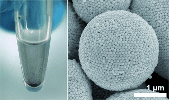
If colloidal gold [gold in solution] self-assembles into the form of larger vesicles, a three-dimensional state can be achieved that is called “black gold” because it absorbs almost the entire spectrum of visible light. How this novel intense plasmonic state can be established and what its characteristics and potential medical applications are is explored by Chinese scientists and reported in the journal Angewandte Chemie …

A July 24, 2015 Wiley (Angewandte Chemie) press release, which originated the news item, provides more details,

Metal nanostructures can self-assemble into superstructures that offer intriguing new spectroscopic and mechanical properties. Plasmonic coupling plays a particular role in this context. For example, it has been found that plasmonic metal nanoparticles help to scatter the incoming light across the surface of the Si substrate at resonance wavelengths, therefore enhancing the light absorbing potential and thus the effectivity of solar cells.

On the other hand, plasmonic vesicles are the promising theranostic platform for biomedical applications, a notion which inspired Yue Li and Cuncheng Li of the Chinese Academy of Science, Hefei, China, and the University of Jinan, China, as well as collaborators to prepare plasmonic colloidosomes composed of gold nanospheres.

As the method of choice, the scientists have designed an emulsion-templating approach based on monodispersed gold nanospheres as building blocks, which arranged themselves into large spherical vesicles in a reverse emulsion system.

The resulting plasmonic vesicles were of micrometer-size and had a shell composed of hexagonally close-packed colloidal nanosphere particles in bilayer or, for the very large superspheres, multilayer arrangement, which provided the enhanced stability.

“A key advantage of this system is that such self-assembly can avoid the introduction of complex stabilization processes to lock the nanoparticles together”, the authors explain.

The hollow spheres exhibited an intense plasmonic resonance in their three-dimensionally packed structure and had a dark black appearance compared to the brick red color of the original gold nanoparticles. The “black gold” was thus characterized by a strong broadband absorption in the visible light and a very regular vesicle superstructure. In medicine, gold vesicles are intensively discussed as vehicles for the drug delivery to tumor cells, and, therefore, it could be envisaged to exploit the specific light-matter interaction of such plasmonic vesicle structures for medical use, but many other applications are also feasible, as the authors propose: “The presented strategy will pave a way to achieve noble-metal superstructures for biosensors, drug delivery, photothermal therapy, optical microcavity, and microreaction platforms.” This will prove the flexibility and versatility of the noble-metal nanostructures.

Here’s a link to and a citation for the paper,

Black Gold: Plasmonic Colloidosomes with Broadband Absorption Self-Assembled from Monodispersed Gold Nanospheres by Using a Reverse Emulsion System by Dilong Liu, Dr. Fei Zhou, Cuncheng Li, Tao Zhang, Honghua Zhang, Prof. Weiping Cai, and Prof. Yue Li. Angewandte Chemie International Edition Article first published online: 25 JUN 2015 DOI: 10.1002/anie.201503384

© 2015 WILEY-VCH Verlag GmbH & Co. KGaA, Weinheim

This article is behind a paywall.

There is an image illustrating the work but, sadly, the gold doesn’t look black,

BlackGold

© Wiley-VCH

That’s it!

Canada and a mandatory survey on nanomaterials due February 2016

If memory serves, this is the second nanomaterials reporting survey that the Canadian federal government has requested in the seven years that I’ve *been* blogging on the topic Canadian nanotechnology. (As usual, I’ve gotten my information from a source outside the country.) Thanks to Lynn Bergeson (US lawyer) and her July 27, 2015 posting on Nanotechnology Now where she covers nanotechnology’s regulatory developments (Note: A link has been removed),

The July 25, 2015, Canada Gazette includes a notice announcing that the Minister of the Environment requires, for the purpose of assessing whether the substances described in the notice are toxic or are capable of becoming toxic, or for the purpose of assessing whether to control, or the manner in which to control the listed substances, any person described in the notice who possesses or who may reasonably be expected to have access to the information required to provide that information. See http://www.gazette.gc.ca/rp-pr/p1/2015/2015-07-25/html/notice-avis-eng.php The notice applies to a substance that has a size of between 1 and 100 nanometers in at least one external dimension, or internal or surface structure; and is provided in the list in Schedule 1 of the notice. The list includes over 200 substances. The notice applies to any person who, during the 2014 calendar year, manufactured a total quantity greater than 100 kilograms (kg) of a substance set out in Schedule 1. …

You can find the Canada Gazette notice (Notice with respect to certain nanomaterials in Canadian commerce) here: http://www.gazette.gc.ca/rp-pr/p1/2015/2015-07-25/html/notice-avis-eng.php but you may find the Guidance for responding to the Notice: http://www.ec.gc.ca/ese-ees/default.asp?lang=En&n=AACFB2C0-1 more helpful (Note: Links have been removed),

1.1- Purpose of the Notice

In 2011, the Canada-United States Regulatory Cooperation Council (RCC) Nanotechnology InitiativeFootnote[1] was launched to increase alignment in regulatory approaches for nanomaterials between Canada and the US to reduce risk to human health and the environment; to promote sharing of scientific and regulatory expertise; and to foster innovation. Completed in February 2014, the RCC Nanotechnology Initiative included a work element on Commercial Information.Footnote[2] This work element was aimed at increasing knowledge of commercial uses of nanomaterials in Canada and the US. The primary output from this work element was a Nanomaterials Use Matrix which identified nanomaterials by type and use category based on the most up-to-date information, at the time, on commercially available nanomaterials. The nanomaterial types were cross-referenced with the DSL to identify nanomaterials which could be considered existing in Canada. The result is a preliminary reference list and may not be comprehensive of all nanomaterials. Ongoing engagement with stakeholders through voluntary initiatives and other fora will inform further development of the list of existing nanomaterials in Canada.

The purpose of the Notice is to gather information on 206 nanomaterials identified as potentially in commerce in Canada from the primary reference list. [emphasis mine] The information collected from the Notice will support the development of a list of nanomaterials in commerce in Canada by confirming their commercial status, and subsequent prioritization activities for these substances, which may include risk assessment and risk management activities, if required. This will ensure that future decision making is based on the best available information.

The list of reportable substances is long and not alphabetized but before you check you may want to review this,

2.1- Reporting criteria

To determine whether a company is required to respond, the following factors must be considered:

Type of substance (i.e., nanoscale form)
Type of activity
Calendar year
Quantity
The quantity should be determined based on the quantity of the substance itself at the nanoscale, and not on the quantity of the product or mixture containing the substance.

The purpose of the Notice is to gather information on nanomaterials in commerce in Canada. A response is only required if the conditions set out in Schedule 1 and Schedule 2 of the notice are met.

The Notice applies to any person who, during the 2014 calendar year [emphasis mine], satisfied any of the following criteria:

Manufactured a total quantity greater than 100 kg of a substance listed in Schedule 1 that is at the nanoscale.
Imported a total quantity greater than 100 kg of a substance listed in Schedule 1 that is at the nanoscale, at any concentration, whether alone, in a mixture or in a product.

The reporting threshold of 100 kg is based on activity with the substance in the nanoscale (i.e. you manufacture, or imported a total quantity greater than 100 kg of a substance with a size between 1 and 100 nanometres, inclusive, in at least one external dimension, or internal or surface structure).

Your response to the information requested should also be based on activities with the substance in the nanoscale.

If you are engaged with a substance that is not in the nanoscale (i.e. same CAS RN, but not nanoscale) and would like to identify yourself as a stakeholder for that substance, you may submit a Declaration of Stakeholder Interest (see section 7 of this document).

You may find this flowchart (from the guidance webpage), useful,

Figure 1: Reporting Diagram for Nanomaterials [downloaded from: http://www.ec.gc.ca/ese-ees/default.asp?lang=En&n=AACFB2C0-1]

Figure 1: Reporting Diagram for Nanomaterials [downloaded from: http://www.ec.gc.ca/ese-ees/default.asp?lang=En&n=AACFB2C0-1]

The information you provide needs to cover the 2014 calendar year and is due,

10. Responding to the Notice

Responses to the Notice must be provided no later than February 23, 2016, 5 p.m. Eastern Standard Time using the online reporting system available through Environment Canada’s Single Window available from the Chemical Substances Web site.

Good luck to all those who must report.

*’been’ added on Jan. 13, 2017.

Commercializing Titan Spine’s next generation spinal interbody fusion implant

The July 22, 2015 Titan Spine news release on BusinessWire is mainly focused on the appointment of a senior nanotechnology specialist; I’m more interested in the mention of product commercialization (first mentioned in my Nov. 26, 2014 post) in the fourth quarter of 2015,

Titan Spine, a medical device surface technology company focused on developing innovative spinal interbody fusion implants, today announced the appointment of Jim Sevey as the Company’s Senior Nanotechnology Specialist. The appointment follows the Company’s receipt of 510(k) clearance from the U.S. Food and Drug Administration (FDA) to market its Endoskeleton® line of interbody fusion implants featuring its next generation nanoLOCKTM surface technology and precedes the Company’s full commercialization of the new line, planned for the fourth quarter of this year. The nanoLOCK™ surface represents the only FDA-cleared nanotechnology for spinal implant applications.

Mr. Sevey’s role will include leading the educational initiatives to further demonstrate and communicate the scientific evidence supporting the advantages of Titan Spine’s unique nanoLOCKTM surface technology. The surface features an increased amount of nano-scaled textures that result in the up-regulation of a greater amount of osteogenic and angiogenic growth factors critical for bone growth and fusion as compared to PEEK and the company’s current surface.1

Kevin Gemas, President of Titan Spine, commented, “As our body of science continues to grow, we identified the need to bring onboard someone of Jim’s caliber to educate the spinal surgeon community and our sales force on the science and associated benefits of our current and nanoLOCK™ proprietary surface technologies. With more than 22 years of experience with medical devices and biomaterials, Jim is the right person to lead these efforts. One of Jim’s initial tasks will be to clearly differentiate the science of our nanotechnology platform from those that claim to have nanotechnology but have not been cleared by the FDA to do so. We are proud to add Jim to our ever-growing scientific team.”

Barbara Boyan, Ph.D., Dean of the School of Engineering at Virginia Commonwealth University, and lead author of several studies supporting Titan Spine surfaces, added, “The spine industry is beginning to recognize ‘nanotechnology’ as more than a marketing concept and now as a design approach that has the potential to improve spinal fusion results for patients. Titan Spine has been at the forefront of this charge for nearly a decade, conducting studies to evaluate and refine the benefits of nanotechnology for interbody fusions. I look forward to working closely with Jim to further these efforts.”

Before joining Titan Spine, Mr. Sevey held several positions at Synthes/Depuy Biomaterials, including most recently, Manager, Biomaterials Technical Specialist. In this role, he generated multidivisional sales of osteobiologic product lines by providing clinical and technical consulting, training, and education for surgeons, residents, operating room personnel, and sales consultants. Prior to Synthes/Depuy Biomaterials, Mr. Sevey was part of the founding team of Skeletal Kinetics, LLC, (Cupertino, CA) as Director of Marketing. Mr. Sevey holds a Bachelor of Science in Health Science from St. Mary’s College of California (Moraga, CA).

The full line of Endoskeleton® devices features Titan Spine’s proprietary implant surface technology, consisting of a unique combination of roughened topographies at the macro, micro, and cellular levels. This unique combination of surface topographies is designed to create an optimal host-bone response and actively participate in the fusion process by promoting the up-regulation of osteogenic and angiogenic factors necessary for bone growth, encouraging natural production of bone morphogenetic proteins (BMPs), down-regulating inflammatory factors, and creating the potential for a faster and more robust fusion.2,3,4

About Titan Spine

Titan Spine, LLC is a surface technology company focused on the design and manufacture of interbody fusion devices for the spine. The company is committed to advancing the science of surface engineering to enhance the treatment of various pathologies of the spine that require fusion. Titan Spine, located in Mequon, Wisconsin and Laichingen, Germany, markets a full line of Endoskeleton® interbody devices featuring its proprietary textured surface in the U.S. and portions of Europe through its sales force and a network of independent distributors. To learn more, visit www.titanspine.com.

Titan Spine Study References:

1 Olivares-Navarrete, R., Hyzy, S. L., Berg, M. E., Schneider, J. M., Hotchkiss, K., Schwartz, Z., & Boyan, B. D. Osteoblast Lineage Cells Can Discriminate Microscale Topographic Features on Titanium–Aluminum–Vanadium Surfaces.Ann Biomed Eng. 2014; 1-11.

2 Olivares-Navarrete, R., Hyzy, S.L., Slosar, P.J., Schneider, J.M., Schwartz, Z., and Boyan, B.D. (2015). Implant materials generate different peri-implant inflammatory factors: PEEK promotes fibrosis and micro-textured titanium promotes osteogenic factors. Spine, Volume 40, Issue 6, 399–404.

3 Olivares-Navarrete, R., Gittens, R.A., Schneider, J.M., Hyzy, S.L., Haithcock, D.A., Ullrich, P.F., Schwartz, Z., Boyan, B.D. (2012). Osteoblasts exhibit a more differentiated phenotype and increased bone morphogenetic production on titanium alloy substrates than poly-ether-ether-ketone. The Spine Journal, 12, 265-272.

4 Olivares-Navarrete, R., Hyzy, S.L., Gittens, R.A., Schneider, J.M., Haithcock, D.A., Ullrich, P.F., Slosar, P. J., Schwartz, Z., Boyan, B.D. (2013). Rough titanium alloys regulate osteoblast production of angiogenic factors. The Spine Journal, 13, 1563-1570.

It’s unusual (and welcome) to see citations included with a business news release for a new medical device.

I didn’t think to pose the query in my last post but I wonder if Barbara Boyan has some sort of financial interest in Titan Spine? Her Virginia Commonwealth University faculty webpage suggests the answer is no,

Experience

  • Associate Dean for Research and Innovation in the College of Engineering at Georgia Institute of Technology
  • Professor and Price Gilbert, Jr. Chair in Tissue Engineering in the Wallace H. Coulter Department of Biomedical Engineering at Georgia Tech and Emory University
  • Deputy Director of Research at Georgia Tech and at the Emory Center for the Engineering of Living Tissues at the Georgia Institute of Technology
  • Professor and Vice Chair for Research in the Department of Orthopaedics at the University of Texas Health Science Center at San Antonio
  • Co-founder of Osteobiologics, Inc.
  • Founder and Chief Scientific Officer of SpherIngenics, Inc.
  • Member, Board of Directors, ArthroCare Corporation and Carticept Medical, Inc.

Still, I wish there was a statement that spelled out Boyan’s relationship or lack of with Titan Spine.

Smart windows from Texas (US)

I’ve been waiting for ‘smart’ windows and/or self-cleaning windows since 2008. While this research on ‘smart’ windows at the University of Texas at Austin looks promising I suspect it will be years before these things are in the marketplace. A July 22, 2015 news item on Nanotechnology Now announces the latest research,

Researchers in the Cockrell School of Engineering at The University of Texas at Austin are one step closer to delivering smart windows with a new level of energy efficiency, engineering materials that allow windows to reveal light without transferring heat and, conversely, to block light while allowing heat transmission, as described in two new research papers.

By allowing indoor occupants to more precisely control the energy and sunlight passing through a window, the new materials could significantly reduce costs for heating and cooling buildings.

In 2013, chemical engineering professor Delia Milliron and her team became the first to develop dual-band electrochromic materials that blend two materials with distinct optical properties for selective control of visible and heat-producing near-infrared light (NIR). In a 2013 issue of Nature, Milliron’s research group demonstrated how, using a small jolt of electricity, a nanocrystal material could be switched back and forth, enabling independent control of light and energy.

A July 23, 2015 University of Texas at Austin news release, which originated the news item, provides more details about the research which has spawned two recently published papers,

The team now has engineered two new advancements in electrochromic materials — a highly selective cool mode and a warm mode — not thought possible several years ago.

The cool mode material is a major step toward a commercialized product because it enables control of 90 percent of NIR and 80 percent of the visible light from the sun and takes only minutes to switch between modes. The previously reported material could require hours.

To achieve this high performance, Milliron and a team, including Cockrell School postdoctoral researcher Jongwook Kim and collaborator Brett Helms of the Lawrence Berkeley National Lab, developed a new nanostructured architecture for electrochromic materials that allows for a cool mode to block near-infrared light while allowing the visible light to shine through. This could help reduce energy costs for cooling buildings and homes during the summer. The researchers reported the new architecture in Nano Letters on July 20.

“We believe our new architected nanocomposite could be seen as a model material, establishing the ideal design for a dual-band electrochromic material,” Milliron said. “This material could be ideal for application as a smart electrochromic window for buildings.”

In the paper, the team demonstrates how the new material can strongly and selectively modulate visible light and NIR by applying a small voltage.

To optimize the performance of electrochromics for practical use, the team organized the two components of the composite material to create a porous interpenetrating network. The framework architecture provides channels for transport of electronic and ionic change. This organization enables substantially faster switching between modes.
Smart Window

The researchers are now working to produce a similarly structured nanocomposite material by simple methods, suitable for low-cost manufacturing.

In a second research paper, Milliron and her team, including Cockrell School graduate student Clayton Dahlman, have reported a proof-of-concept demonstrating how they can achieve optical control properties in windows from a well-crafted, single-component film. The concept includes a simple coating that creates a new warm mode, in which visible light can be blocked, while near-infrared light can enter. This new setting could be most useful on a sunny winter day, when an occupant would want infrared radiation to pass into a building for warmth, but the glare from sunlight to be reduced.

In this paper, published in the Journal of the American Chemical Society, Milliron proved that a coating containing a single component ­— doped titania nanocrystals — could demonstrate dynamic control over the transmittance of solar radiation. Because of two distinct charging mechanisms found at different applied voltages, this material can selectively block visible or infrared radiation.

“These two advancements show that sophisticated dynamic control of sunlight is possible,” Milliron said. “We believe our deliberately crafted nanocrystal-based materials could meet the performance and cost targets needed to progress toward commercialization of smart windows.”

Interestingly, the news release includes this statement,

The University of Texas at Austin is committed to transparency and disclosure of all potential conflicts of interest. The lead UT investigator involved with this project, Delia Milliron, is the chief scientific officer and owns an equity position in Heliotrope Technologies, an early-stage company developing new materials and manufacturing processes for electrochromic devices with an emphasis on energy-saving smart windows. Milliron is associated with patents at Lawrence Berkeley National Laboratory licensed to Heliotrope Technologies. Collaborator Brett Helms serves on the scientific advisory board of Heliotrope and owns equity in the company.

Here are links to and citations for the two papers,

Nanocomposite Architecture for Rapid, Spectrally-Selective Electrochromic Modulation of Solar Transmittance by Jongwook Kim, Gary K. Ong, Yang Wang, Gabriel LeBlanc, Teresa E. Williams, Tracy M. Mattox, Brett A. Helms, and Delia J. Milliron. Nano Lett., Article ASAP DOI: 10.1021/acs.nanolett.5b02197 Publication Date (Web): July 20, 2015

Copyright © 2015 American Chemical Society

Spectroelectrochemical Signatures of Capacitive Charging and Ion Insertion in Doped Anatase Titania Nanocrystals by Clayton J. Dahlman, Yizheng Tan, Matthew A. Marcus, and Delia J. Milliron. J. Am. Chem. Soc., 2015, 137 (28), pp 9160–9166 DOI: 10.1021/jacs.5b04933 Publication Date (Web): July 8, 2015

Copyright © 2015 American Chemical Society

These papers are behind paywalls.