Tag Archives: silver

A deep look at atomic switches

A July 19, 2019 news item on phys.org describes research that may result in a substantive change for information technology,

A team of researchers from Tokyo Institute of Technology has gained unprecedented insight into the inner workings of an atomic switch. By investigating the composition of the tiny metal ‘bridge’ that forms inside the switch, their findings may spur the design of atomic switches with improved performance.

A July 22, 2019 Tokyo Institute of Technology press release (also on EurekAlert but published July 19, 2019), which originated the news item, explains how this research could have such an important impact,

Atomic switches are hailed as the tiniest of electrochemical switches that could change the face of information technology. Due to their nanoscale dimensions and low power consumption, they hold promise for integration into next-generation circuits that could drive the development of artificial intelligence (AI) and Internet of Things (IoT) devices.

Although various designs have emerged, one intriguing question concerns the nature of the metallic filament, or bridge, that is key to the operation of the switch. The bridge forms inside a metal sulfide layer sandwiched between two electrodes [see figure below], and is controlled by applying a voltage that induces an electrochemical reaction. The formation and annihilation of this bridge determines whether the switch is on or off.

Now, a research group including Akira Aiba and Manabu Kiguchi and colleagues at Tokyo Institute of Technology’s Department of Chemistry has found a useful way to examine precisely what the bridge is composed of.

By cooling the atomic switch enough so as to be able to investigate the bridge using a low-temperature measurement technique called point contact spectroscopy (PCS) [2], their study revealed that the bridge is made up of metal atoms from both the electrode and the metal sulfide layer. This surprising finding controverts the prevailing notion that the bridge derives from the electrode only, Kiguchi explains.

The team compared atomic switches with different combinations of electrodes (Pt and Ag, or Pt and Cu) and metal sulfide layers (Cu2S and Ag2S). In both cases, they found that the bridge is mainly composed of Ag.

The reason behind the dominance of Ag in the bridge is likely due to “the higher mobility of Ag ions compared to Cu ions”, the researchers say in their paper published in ACS Applied Materials & Interfaces.

They conclude that “it would be better to use metals with low mobility” for designing atomic switches with higher stability.

Much remains to be explored in the advancement of atomic switch technologies, and the team is continuing to investigate which combination of elements would be the most effective in improving performance.

###

Technical terms
[1] Atomic switch: The idea behind an atomic switch — one that can be controlled by the motion of a single atom — was introduced by Donald Eigler and colleagues at the IBM Almaden Research Center in 1991. Interest has since focused on how to realize and harness the potential of such extremely small switches for use in logic circuits and memory devices. Over the past two decades, researchers in Japan have taken a world-leading role in the development of atomic switch technologies.
[2] Point contact spectroscopy: A method of measuring the properties or excitations of single atoms at low temperature.

Caption: The ‘bridge’ that forms within the metal sulfide layer, connecting two metal electrodes, results in the atomic switch being turned on. Credit: Manabu Kiguchi

Here’s a link to and a citation for the paper,

Investigation of Ag and Cu Filament Formation Inside the Metal Sulfide Layer of an Atomic Switch Based on Point-Contact Spectroscopy by A. Aiba, R. Koizumi, T. Tsuruoka, K. Terabe, K. Tsukagoshi, S. Kaneko, S. Fujii, T. Nishino, M. Kiguchi. ACS Appl. Mater. Interfaces 2019 XXXXXXXXXX-XXX DOI: https://doi.org/10.1021/acsami.9b05523 Publication Date:July 5, 2019 Copyright © 2019 American Chemical Society

This paper is behind a paywall.

For anyone who might need a bit of a refresher for the chemical elements, Pt is platinum, Ag is silver, and Cu is copper. So, with regard to the metal sulfide layers Cu2S is copper sulfide and Ag2S is silver sulfide.

Borophene and next generation electronics?

2D materials as signified by the ‘ene’ suffix are, as far as I can tell, always associated with electronics—initially. Borophene is not an exception.

This borophene news was announced in a December 3, 2018 news item on ScienceDaily,

Borophene — two-dimensional (2-D) atom-thin-sheets of boron, a chemical element traditionally found in fiberglass insulation — is anything but boring. Though boron is a nonmetallic semiconductor in its bulk (3-D) form, it becomes a metallic conductor in 2-D. Borophene is extremely flexible, strong, and lightweight — even more so than its carbon-based analogue, graphene. [Providing a little competition to the Europeans who are seriously pursuing nanotechnology-enabled electronics and other applications with graphene?] These unique electronic and mechanical properties make borophene a promising material platform for next-generation electronic devices such as wearables, biomolecule sensors, light detectors, and quantum computers.

Now, physicists from the U.S. Department of Energy’s (DOE) Brookhaven National Laboratory and Yale University have synthesized borophene on copper substrates with large-area (ranging in size from 10 to 100 micrometers) single-crystal domains (for reference, a strand of human hair is about 100 micrometers wide). Previously, only nanometer-size single-crystal flakes of borophene had been produced. The advance, reported on Dec. 3 [2018] in Nature Nanotechnology, represents an important step in making practical borophene-based devices possible.

A December 3, 2018 Brookhaven National Laboratory (BNL) news release (also on EurekAlert), which originated the news item, provides more detail about 2D materials and the specifics of this borophene research,

For electronic applications, high-quality single crystals–periodic arrangements of atoms that continue throughout the entire crystal lattice without boundaries or defects–must be distributed over large areas of the surface material (substrate) on which they are grown. For example, today’s microchips use single crystals of silicon and other semiconductors. Device fabrication also requires an understanding of how different substrates and growth conditions impact a material’s crystal structure, which determines its properties.

“We increased the size of the single-crystal domains by a factor of a million,” said co-author and project lead Ivan Bozovic, senior scientist and Molecular Beam Epitaxy Group Leader in Brookhaven Lab’s Condensed Matter Physics and Materials Science (CMPMS) Department and adjunct professor of applied physics at Yale University. “Large domains are required to fabricate next-generation electronic devices with high electron mobility. Electrons that can easily and quickly move through a crystal structure are key to improving device performance.”

A new 2-D material

Since the 2004 discovery of graphene–a single sheet of carbon atoms, which can be peeled from graphite, the core component of pencils, with Scotch tape–scientists have been on the hunt for other 2-D materials with remarkable properties. The chemical bonds between carbon atoms that impart graphene with its strength make manipulating its structure difficult.

Theorists predicted that boron (next to carbon on the Periodic Table, with one less electron) deposited on an appropriately chosen substrate could form a 2-D material similar to graphene. But this prediction was not experimentally confirmed until three years ago, when scientists synthesized borophene for the very first time. They deposited boron onto silver substrates under ultrahigh-vacuum conditions through molecular beam epitaxy (MBE), a precisely controlled atomic layer-by-layer crystal growth technique. Soon thereafter, another group of scientists grew borophene on silver, but they proposed an entirely different crystal structure.

“Borophene is structurally similar to graphene, with a hexagonal network made of boron (instead of carbon) atoms on each of the six vertices defining the hexagon,” said Bozovic. “However, borophene is different in that it periodically has an extra boron atom in the center of the hexagon. The crystal structure tends to be theoretically stable when about four out of every five center positions are occupied and one is vacant.”

According to theory, while the number of vacancies is fixed, their arrangement is not. As long as the vacancies are distributed in a way that maintains the most stable (lowest energy) structure, they can be rearranged. Because of this flexibility, borophene can have multiple configurations.

A small step toward device fabrication

In this study, the scientists first investigated the real-time growth of borophene on silver surfaces at various temperatures. They grew the samples at Yale in an ultra-high vacuum low-energy electron microscope (LEEM) equipped with an MBE system. During and after the growth process, they bombarded the sample with a beam of electrons at low energy and analyzed the low-energy electron diffraction (LEED) patterns produced as electrons were reflected from the crystal surface and projected onto a detector. Because the electrons have low energy, they can only reach the first few atomic layers of the material. The distance between the reflected electrons (“spots” in the diffraction patterns) is related to the distance between atoms on the surface, and from this information, scientists can reconstruct the crystal structure.

In this case, the patterns revealed that the single-crystal borophene domains were only tens of nanometers in size–too small for fabricating devices and studying fundamental physical properties–for all growth conditions. They also resolved the controversy about borophene’s structure: both structures exist, but they form at different temperatures. The scientists confirmed their LEEM and LEED results through atomic force microscopy (AFM). In AFM, a sharp tip is scanned over a surface, and the measured force between the tip and atoms on the surface is used to map the atomic arrangement.

To promote the formation of larger crystals, the scientists then switched the substrate from silver to copper, applying the same LEEM, LEED, and AFM techniques. Brookhaven scientists Percy Zahl and Ilya Drozdov also imaged the surface structure at high resolution using a custom-built scanning tunneling microscope (STM) with a carbon monoxide probe tip at Brookhaven’s Center for Functional Nanomaterials (CFN)–a U.S. Department of Energy (DOE) Office of Science User Facility. Yale theorists Stephen Eltinge and Sohrab Ismail-Beigi performed calculations to determine the stability of the experimentally obtained structures. After identifying which structures were most stable, they simulated the electron diffraction spectra and STM images and compared them to the experimental data. This iterative process continued until theory and experiment were in agreement.

“From theoretical insights, we expected copper to produce larger single crystals because it interacts more strongly with borophene than silver,” said Bozovic. “Copper donates some electrons to stabilize borophene, but the materials do not interact too much as to form a compound. Not only are the single crystals larger, but the structures of borophene on copper are different from any of those grown on silver.”

Because there are several possible distributions of vacancies on the surface, various crystal structures of borophene can emerge. This study also showed how the structure of borophene can be modified by changing the substrate and, in some cases, the temperature or deposition rate.

The next step is to transfer the borophene sheets from the metallic copper surfaces to insulating device-compatible substrates. Then, scientists will be able to accurately measure resistivity and other electrical properties important to device functionality. Bozovic is particularly excited to test whether borophene can be made superconducting. Some theorists have speculated that its unusual electronic structure may even open a path to lossless transmission of electricity at room temperature, as opposed to the ultracold temperatures usually required for superconductivity. Ultimately, the goal in 2-D materials research is to be able to fine-tune the properties of these materials to suit particular applications.

Here’s a link to and a citation for the paper,

Large-area single-crystal sheets of borophene on Cu(111) surfaces by Rongting Wu, Ilya K. Drozdov, Stephen Eltinge, Percy Zahl, Sohrab Ismail-Beigi, Ivan Božović & Adrian Gozar. Nature Nanotechnology (2018) DOI: https://doi.org/10.1038/s41565-018-0317-6Published 03 December 2018

This paper is behind a paywall.

A solar, self-charging supercapacitor for wearable technology

Ravinder Dahiya, Carlos García Núñez, and their colleagues at the University of Glasgow (Scotland) strike again (see my May 10, 2017 posting for their first ‘solar-powered graphene skin’ research announcement). Last time it was all about robots and prosthetics, this time they’ve focused on wearable technology according to a July 18, 2018 news item on phys.org,

A new form of solar-powered supercapacitor could help make future wearable technologies lighter and more energy-efficient, scientists say.

In a paper published in the journal Nano Energy, researchers from the University of Glasgow’s Bendable Electronics and Sensing Technologies (BEST) group describe how they have developed a promising new type of graphene supercapacitor, which could be used in the next generation of wearable health sensors.

A July 18, 2018 University of Glasgow press release, which originated the news item, explains further,

Currently, wearable systems generally rely on relatively heavy, inflexible batteries, which can be uncomfortable for long-term users. The BEST team, led by Professor Ravinder Dahiya, have built on their previous success in developing flexible sensors by developing a supercapacitor which could power health sensors capable of conforming to wearer’s bodies, offering more comfort and a more consistent contact with skin to better collect health data.

Their new supercapacitor uses layers of flexible, three-dimensional porous foam formed from graphene and silver to produce a device capable of storing and releasing around three times more power than any similar flexible supercapacitor. The team demonstrated the durability of the supercapacitor, showing that it provided power consistently across 25,000 charging and discharging cycles.

They have also found a way to charge the system by integrating it with flexible solar powered skin already developed by the BEST group, effectively creating an entirely self-charging system, as well as a pH sensor which uses wearer’s sweat to monitor their health.

Professor Dahiya said: “We’re very pleased by the progress this new form of solar-powered supercapacitor represents. A flexible, wearable health monitoring system which only requires exposure to sunlight to charge has a lot of obvious commercial appeal, but the underlying technology has a great deal of additional potential.

“This research could take the wearable systems for health monitoring to remote parts of the world where solar power is often the most reliable source of energy, and it could also increase the efficiency of hybrid electric vehicles. We’re already looking at further integrating the technology into flexible synthetic skin which we’re developing for use in advanced prosthetics.” [emphasis mine]

In addition to the team’s work on robots, prosthetics, and graphene ‘skin’ mentioned in the May 10, 2017 posting the team is working on a synthetic ‘brainy’ skin for which they have just received £1.5m funding from the Engineering and Physical Science Research Council (EPSRC).

Brainy skin

A July 3, 2018 University of Glasgow press release discusses the proposed work in more detail,

A robotic hand covered in ‘brainy skin’ that mimics the human sense of touch is being developed by scientists.

University of Glasgow’s Professor Ravinder Dahiya has plans to develop ultra-flexible, synthetic Brainy Skin that ‘thinks for itself’.

The super-flexible, hypersensitive skin may one day be used to make more responsive prosthetics for amputees, or to build robots with a sense of touch.

Brainy Skin reacts like human skin, which has its own neurons that respond immediately to touch rather than having to relay the whole message to the brain.

This electronic ‘thinking skin’ is made from silicon based printed neural transistors and graphene – an ultra-thin form of carbon that is only an atom thick, but stronger than steel.

The new version is more powerful, less cumbersome and would work better than earlier prototypes, also developed by Professor Dahiya and his Bendable Electronics and Sensing Technologies (BEST) team at the University’s School of Engineering.

His futuristic research, called neuPRINTSKIN (Neuromorphic Printed Tactile Skin), has just received another £1.5m funding from the Engineering and Physical Science Research Council (EPSRC).

Professor Dahiya said: “Human skin is an incredibly complex system capable of detecting pressure, temperature and texture through an array of neural sensors that carry signals from the skin to the brain.

“Inspired by real skin, this project will harness the technological advances in electronic engineering to mimic some features of human skin, such as softness, bendability and now, also sense of touch. This skin will not just mimic the morphology of the skin but also its functionality.

“Brainy Skin is critical for the autonomy of robots and for a safe human-robot interaction to meet emerging societal needs such as helping the elderly.”

Synthetic ‘Brainy Skin’ with sense of touch gets £1.5m funding. Photo of Professor Ravinder Dahiya

This latest advance means tactile data is gathered over large areas by the synthetic skin’s computing system rather than sent to the brain for interpretation.

With additional EPSRC funding, which extends Professor Dahiya’s fellowship by another three years, he plans to introduce tactile skin with neuron-like processing. This breakthrough in the tactile sensing research will lead to the first neuromorphic tactile skin, or ‘brainy skin.’

To achieve this, Professor Dahiya will add a new neural layer to the e-skin that he has already developed using printing silicon nanowires.

Professor Dahiya added: “By adding a neural layer underneath the current tactile skin, neuPRINTSKIN will add significant new perspective to the e-skin research, and trigger transformations in several areas such as robotics, prosthetics, artificial intelligence, wearable systems, next-generation computing, and flexible and printed electronics.”

The Engineering and Physical Sciences Research Council (EPSRC) is part of UK Research and Innovation, a non-departmental public body funded by a grant-in-aid from the UK government.

EPSRC is the main funding body for engineering and physical sciences research in the UK. By investing in research and postgraduate training, the EPSRC is building the knowledge and skills base needed to address the scientific and technological challenges facing the nation.

Its portfolio covers a vast range of fields from healthcare technologies to structural engineering, manufacturing to mathematics, advanced materials to chemistry. The research funded by EPSRC has impact across all sectors. It provides a platform for future UK prosperity by contributing to a healthy, connected, resilient, productive nation.

It’s fascinating to note how these pieces of research fit together for wearable technology and health monitoring and creating more responsive robot ‘skin’ and, possibly, prosthetic devices that would allow someone to feel again.

The latest research paper

Getting back the solar-charging supercapacitors mentioned in the opening, here’s a link to and a citation for the team’s latest research paper,

Flexible self-charging supercapacitor based on graphene-Ag-3D graphene foam electrodes by Libu Manjakka, Carlos García Núñez, Wenting Dang, Ravinder Dahiya. Nano Energy Volume 51, September 2018, Pages 604-612 DOI: https://doi.org/10.1016/j.nanoen.2018.06.072

This paper is open access.

Panning for silver nanoparticles in your clothes washer

A March 20, 2018 news item on phys.org describes a new approach to treating wastewater (Note: Links have been removed),

Humans have known since ancient times that silver kills or stops the growth of many microorganisms. Hippocrates, the father of medicine, is said to have used silver preparations for treating ulcers and healing wounds. Until the introduction of antibiotics in the 1940s, colloidal silver (tiny particles suspended in a liquid) was a mainstay for treating burns, infected wounds and ulcers. Silver is still used today in wound dressings, in creams and as a coating on medical devices.

Since the 1990s, manufacturers have added silver nanoparticles to numerous consumer products to enhance their antibacterial and anti-odor properties. Examples include clothes, towels, undergarments, socks, toothpaste and soft toys. Nanoparticles are ultra-small particles, ranging from 1 to 100 nanometers in diameter – too small to see even with a microscope. According to a widely cited database, about one-fourth of nanomaterial-based consumer products currently marketed in the United States contain nanosilver.

Multiple studies have reported that nanosilver leaches out of textiles when they are laundered. Research also reveals that nanosilver may be toxic to humans and aquatic and marine organisms. Although it is widely used, little is understood about its fate or long-term toxic effects in the environment.

We are developing ways to convert this potential ecological crisis into an opportunity by recovering pure silver nanoparticles, which have many industrial applications, from laundry wastewater. In a recently published study, we describe a technique for silver recovery and discuss the key technical challenges. Our approach tackles this problem at the source – in this case, individual washing machines. We believe that this strategy has great promise for getting newly identified contaminants out of wastewater.

A March 20, 2018 essay by Sukalyan Sengupta, Professor of Wastewater Treatment, and Tabish Nawaz. Doctoral Student, both at University of Massachusetts at Dartmouth on The Conversation website, which originated the news item, expands on the theme (Note: Links have been removed),

Use of nanosilver in consumer products has steadily risen in the past decade. The market share of silver-based textiles rose from 9 percent in 2004 to 25 percent in 2011.

Several investigators have measured the silver content of textiles and found values ranging from 0.009 to 21,600 milligrams of silver per kilogram of textile. Studies show that the amount of silver leached in the wash solution depends on many factors, including interactions between detergent and other chemicals and how silver is attached to the textiles.

In humans, exposure to silver can harm liver cells, skin and lungs. Prolonged exposure or exposure to a large dose can cause a condition called Argyria, in which the victim’s skin turns permanently bluish-gray.

Once silver goes down the drain and ends up at wastewater treatment plants, it can potentially harm bacterial treatment processes, making them less efficient, and foul treatment equipment. More than 90 percent of silver nanoparticles released in wastewater end up in nutrient-rich biosolids left over at the end of sewage treatment, which often are used on land as agricultural fertilizers.

Silver is toxic in aquatic environments, a concern that’s becoming more serious with the increased use of silver nanoparticles and awareness that oceans, rivers, and lakes are dangerously stressed.

Sengupta and Nawaz go on to describe their proposed solution (Note: Links have been removed),

Our research shows that the most efficient way to remove silver from wastewater is by treating it in the washing machine. At this point silver concentrations are relatively high, and silver is initially released from treated clothing in a chemical form that is feasible to recover.

A bit of chemistry is helpful here. Our recovery method employs a widely used chemistry process called ion exchange. Ions are atoms or molecules that have an electrical charge. In ion exchange, a solid and a liquid are brought together and exchange ions with each other.

For example, household soaps do not lather well in “hard” water, which contains high levels of ions such as magnesium and calcium. Many home water filters use ion exchange to “soften” the water, replacing those materials with other ions that do not affect its properties in the same way.

For this process to work, the ions that switch places must both be either positively or negatively charged. Nanosilver is initially released from textiles as silver ion, which is a cation – an ion with a positive charge (hence the plus sign in its chemical symbol, Ag+).

Even at the source, removing silver from washwater is challenging. Silver concentrations in the wash solution are relatively low compared to other cations, such as calcium, that could interfere with the removal process. Detergent chemistry complicates the picture further because some detergent components can potentially interact with silver.

To recover silver without picking up other chemicals, the recovery process must use materials that have a chemical affinity for silver. In a previous study, we described a potential solution: Using ion-exchange materials embedded with sulfur-based chemicals, which bind preferentially with silver.

In our new study, we passed washwater through an ion-exchange resin column and analyzed how each major detergent ingredient interacted with silver in the water and affected the resin’s ability to remove silver from the water. By manipulating process conditions such as pH, temperature and concentration of nonsilver cations, we were able to identify conditions that maximized silver recovery.

We found that pH and the levels of calcium ions (Ca2+) were critical factors. Higher levels of hydrogen or calcium ions bind up detergent ingredients and prevent them from interacting with silver ions, so the ion-exchange resin can remove the silver from the solution. We also found that some detergent ingredients – particularly bleaching and water-softening agents – made the ion-exchange resin work less efficiently. Depending on these conditions, we recovered between 20 percent and 99 percent of the silver in the washwater.

The researchers go on to propose a new approach to treating wastewater (Note: A link has been removed),

Today wastewater is collected from multiple sources, such as homes and businesses, and piped over long distances to centralized wastewater treatment plants. But increasing evidence shows that these facilities are ill-equipped to keep newly identified contaminants out of the environment, since they use one common treatment scheme for many different waste streams.

We believe the future is in decentralized systems that can treat different types of wastewater with specific technologies designed specifically for the materials they contain. If wastewater from laundromats contains different contaminants than wastewater from restaurants, why treat them the same way?

Interesting, non? In any event, here’s a link to and a citation for what I believe is the researchers’ latest paper on this subject,

Silver Recovery from Laundry Washwater: The Role of Detergent Chemistry by Tabish Nawaz and Sukalyan Sengupta. ACS Sustainable Chem. Eng., 2018, 6 (1), pp 600–608 DOI: 10.1021/acssuschemeng.7b02933 Publication Date (Web): November 21, 2017

Copyright © 2017 American Chemical Society

This paper is behind a paywall. For anyone who can’t get access, Karla Lant provides a bit more technical detail about the work in her February 2, 2018 article for fondriest.com.

Gold’s origin in the universe due to cosmic collision

An hypothesis for gold’s origins was first mentioned here in a May 26, 2016 posting,

The link between this research and my side project on gold nanoparticles is a bit tenuous but this work on the origins for gold and other precious metals being found in the stars is so fascinating and I’m determined to find a connection.

An artist's impression of two neutron stars colliding. (Credit: Dana Berry / Skyworks Digital, Inc.) Courtesy: Kavli Foundation

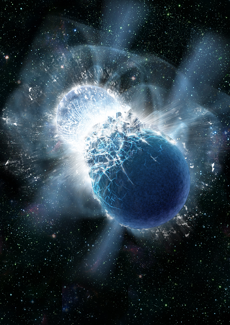
An artist’s impression of two neutron stars colliding. (Credit: Dana Berry / Skyworks Digital, Inc.) Courtesy: Kavli Foundation

From a May 19, 2016 news item on phys.org,

The origin of many of the most precious elements on the periodic table, such as gold, silver and platinum, has perplexed scientists for more than six decades. Now a recent study has an answer, evocatively conveyed in the faint starlight from a distant dwarf galaxy.

In a roundtable discussion, published today [May 19, 2016?], The Kavli Foundation spoke to two of the researchers behind the discovery about why the source of these heavy elements, collectively called “r-process” elements, has been so hard to crack.

From the Spring 2016 Kavli Foundation webpage hosting the  “Galactic ‘Gold Mine’ Explains the Origin of Nature’s Heaviest Elements” Roundtable ,

Astronomers studying a galaxy called Reticulum II have just discovered that its stars contain whopping amounts of these metals—collectively known as “r-process” elements (See “What is the R-Process?”). Of the 10 dwarf galaxies that have been similarly studied so far, only Reticulum II bears such strong chemical signatures. The finding suggests some unusual event took place billions of years ago that created ample amounts of heavy elements and then strew them throughout the galaxy’s reservoir of gas and dust. This r-process-enriched material then went on to form Reticulum II’s standout stars.

Based on the new study, from a team of researchers at the Kavli Institute at the Massachusetts Institute of Technology, the unusual event in Reticulum II was likely the collision of two, ultra-dense objects called neutron stars. Scientists have hypothesized for decades that these collisions could serve as a primary source for r-process elements, yet the idea had lacked solid observational evidence. Now armed with this information, scientists can further hope to retrace the histories of galaxies based on the contents of their stars, in effect conducting “stellar archeology.”

Researchers have confirmed the hypothesis according to an Oct. 16, 2017 news item on phys.org,

Gold’s origin in the Universe has finally been confirmed, after a gravitational wave source was seen and heard for the first time ever by an international collaboration of researchers, with astronomers at the University of Warwick playing a leading role.

Members of Warwick’s Astronomy and Astrophysics Group, Professor Andrew Levan, Dr Joe Lyman, Dr Sam Oates and Dr Danny Steeghs, led observations which captured the light of two colliding neutron stars, shortly after being detected through gravitational waves – perhaps the most eagerly anticipated phenomenon in modern astronomy.

Marina Koren’s Oct. 16, 2017 article for The Atlantic presents a richly evocative view (Note: Links have been removed),

Some 130 million years ago, in another galaxy, two neutron stars spiraled closer and closer together until they smashed into each other in spectacular fashion. The violent collision produced gravitational waves, cosmic ripples powerful enough to stretch and squeeze the fabric of the universe. There was a brief flash of light a million trillion times as bright as the sun, and then a hot cloud of radioactive debris. The afterglow hung for several days, shifting from bright blue to dull red as the ejected material cooled in the emptiness of space.

Astronomers detected the aftermath of the merger on Earth on August 17. For the first time, they could see the source of universe-warping forces Albert Einstein predicted a century ago. Unlike with black-hole collisions, they had visible proof, and it looked like a bright jewel in the night sky.

But the merger of two neutron stars is more than fireworks. It’s a factory.

Using infrared telescopes, astronomers studied the spectra—the chemical composition of cosmic objects—of the collision and found that the plume ejected by the merger contained a host of newly formed heavy chemical elements, including gold, silver, platinum, and others. Scientists estimate the amount of cosmic bling totals about 10,000 Earth-masses of heavy elements.

I’m not sure exactly what this image signifies but it did accompany Koren’s article so presumably it’s a representation of colliding neutron stars,

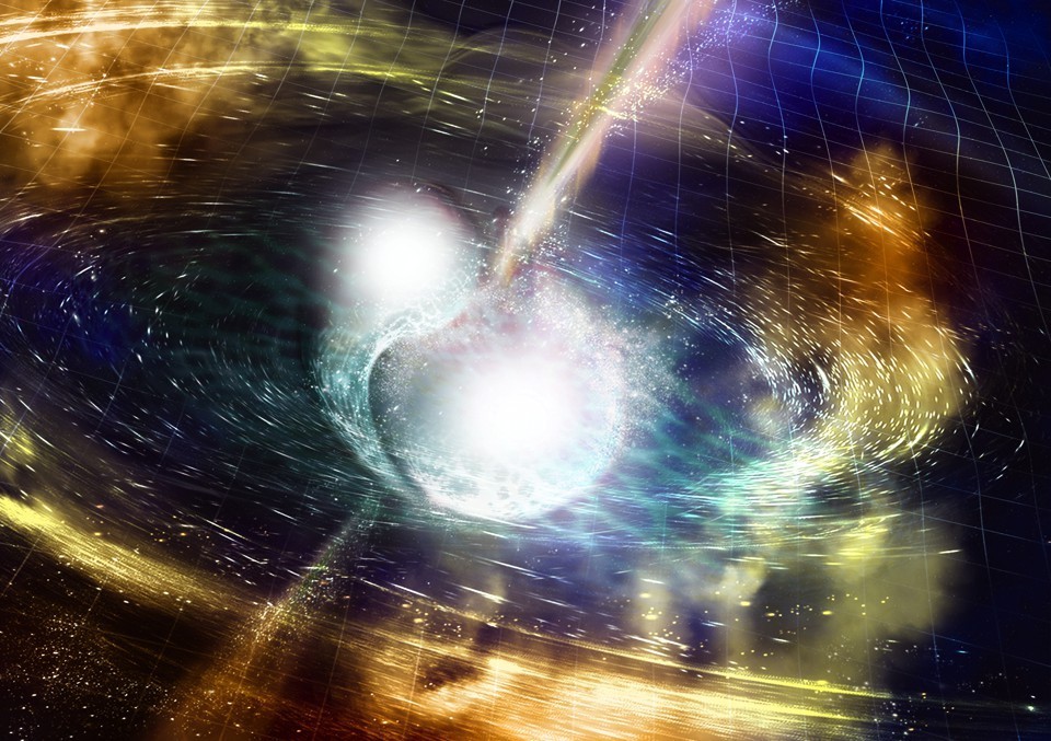
NSF / LIGO / Sonoma State University /A. Simonnet. Downloaded from: https://www.theatlantic.com/science/archive/2017/10/the-making-of-cosmic-bling/543030/

An Oct. 16, 2017 University of Warwick press release (also on EurekAlert), which originated the news item on phys.org, provides more detail,

Huge amounts of gold, platinum, uranium and other heavy elements were created in the collision of these compact stellar remnants, and were pumped out into the universe – unlocking the mystery of how gold on wedding rings and jewellery is originally formed.

The collision produced as much gold as the mass of the Earth. [emphasis mine]

This discovery has also confirmed conclusively that short gamma-ray bursts are directly caused by the merging of two neutron stars.

The neutron stars were very dense – as heavy as our Sun yet only 10 kilometres across – and they collided with each other 130 million years ago, when dinosaurs roamed the Earth, in a relatively old galaxy that was no longer forming many stars.

They drew towards each other over millions of light years, and revolved around each other increasingly quickly as they got closer – eventually spinning around each other five hundred times per second.

Their merging sent ripples through the fabric of space and time – and these ripples are the elusive gravitational waves spotted by the astronomers.

The gravitational waves were detected by the Advanced Laser Interferometer Gravitational-Wave Observatory (Adv-LIGO) on 17 August this year [2017], with a short duration gamma-ray burst detected by the Fermi satellite just two seconds later.

This led to a flurry of observations as night fell in Chile, with a first report of a new source from the Swope 1m telescope.

Longstanding collaborators Professor Levan and Professor Nial Tanvir (from the University of Leicester) used the facilities of the European Southern Observatory to pinpoint the source in infrared light.

Professor Levan’s team was the first one to get observations of this new source with the Hubble Space Telescope. It comes from a galaxy called NGC 4993, 130 million light years away.

Andrew Levan, Professor in the Astronomy & Astrophysics group at the University of Warwick, commented: “Once we saw the data, we realised we had caught a new kind of astrophysical object. This ushers in the era of multi-messenger astronomy, it is like being able to see and hear for the first time.”

Dr Joe Lyman, who was observing at the European Southern Observatory at the time was the first to alert the community that the source was unlike any seen before.

He commented: “The exquisite observations obtained in a few days showed we were observing a kilonova, an object whose light is powered by extreme nuclear reactions. This tells us that the heavy elements, like the gold or platinum in jewellery are the cinders, forged in the billion degree remnants of a merging neutron star.”

Dr Samantha Oates added: “This discovery has answered three questions that astronomers have been puzzling for decades: what happens when neutron stars merge? What causes the short duration gamma-ray bursts? Where are the heavy elements, like gold, made? In the space of about a week all three of these mysteries were solved.”

Dr Danny Steeghs said: “This is a new chapter in astrophysics. We hope that in the next few years we will detect many more events like this. Indeed, in Warwick we have just finished building a telescope designed to do just this job, and we expect it to pinpoint these sources in this new era of multi-messenger astronomy”.

Congratulations to all of the researchers involved in this work!

Many, many research teams were  involved. Here’s a sampling of their news releases which focus on their areas of research,

University of the Witwatersrand (South Africa)

https://www.eurekalert.org/pub_releases/2017-10/uotw-wti101717.php

Weizmann Institute of Science (Israel)

https://www.eurekalert.org/pub_releases/2017-10/wios-cns101717.php

Carnegie Institution for Science (US)

https://www.eurekalert.org/pub_releases/2017-10/cifs-dns101217.php

Northwestern University (US)

https://www.eurekalert.org/pub_releases/2017-10/nu-adc101617.php

National Radio Astronomy Observatory (US)

https://www.eurekalert.org/pub_releases/2017-10/nrao-ru101317.php

Max-Planck-Gesellschaft (Germany)

https://www.eurekalert.org/pub_releases/2017-10/m-gwf101817.php

Penn State (Pennsylvania State University; US)

https://www.eurekalert.org/pub_releases/2017-10/ps-stl101617.php

University of California – Davis

https://www.eurekalert.org/pub_releases/2017-10/uoc–cns101717.php

The American Association for the Advancement of Science’s (AAAS) magazine, Science, has published seven papers on this research. Here’s an Oct. 16, 2017 AAAS news release with an overview of the papers,

https://www.eurekalert.org/pub_releases/2017-10/aaft-btf101617.php

I’m sure there are more news releases out there and that there will be many more papers published in many journals, so if this interests, I encourage you to keep looking.

Two final pieces I’d like to draw your attention to: one answers basic questions and another focuses on how artists knew what to draw when neutron stars collide.

Keith A Spencer’s Oct. 18, 2017 piece on salon.com answers a lot of basic questions for those of us who don’t have a background in astronomy. Here are a couple of examples,

What is a neutron star?

Okay, you know how atoms have protons, neutrons, and electrons in them? And you know how protons are positively charged, and electrons are negatively charged, and neutrons are neutral?

Yeah, I remember that from watching Bill Nye as a kid.

Totally. Anyway, have you ever wondered why the negatively-charged electrons and the positively-charged protons don’t just merge into each other and form a neutral neutron? I mean, they’re sitting there in the atom’s nucleus pretty close to each other. Like, if you had two magnets that close, they’d stick together immediately.

I guess now that you mention it, yeah, it is weird.

Well, it’s because there’s another force deep in the atom that’s preventing them from merging.

It’s really really strong.

The only way to overcome this force is to have a huge amount of matter in a really hot, dense space — basically shove them into each other until they give up and stick together and become a neutron. This happens in very large stars that have been around for a while — the core collapses, and in the aftermath, the electrons in the star are so close to the protons, and under so much pressure, that they suddenly merge. There’s a big explosion and the outer material of the star is sloughed off.

Okay, so you’re saying under a lot of pressure and in certain conditions, some stars collapse and become big balls of neutrons?

Pretty much, yeah.

So why do the neutrons just stick around in a huge ball? Aren’t they neutral? What’s keeping them together? 

Gravity, mostly. But also the strong nuclear force, that aforementioned weird strong force. This isn’t something you’d encounter on a macroscopic scale — the strong force only really works at the type of distances typified by particles in atomic nuclei. And it’s different, fundamentally, than the electromagnetic force, which is what makes magnets attract and repel and what makes your hair stick up when you rub a balloon on it.

So these neutrons in a big ball are bound by gravity, but also sticking together by virtue of the strong nuclear force. 

So basically, the new ball of neutrons is really small, at least, compared to how heavy it is. That’s because the neutrons are all clumped together as if this neutron star is one giant atomic nucleus — which it kinda is. It’s like a giant atom made only of neutrons. If our sun were a neutron star, it would be less than 20 miles wide. It would also not be something you would ever want to get near.

Got it. That means two giant balls of neutrons that weighed like, more than our sun and were only ten-ish miles wide, suddenly smashed into each other, and in the aftermath created a black hole, and we are just now detecting it on Earth?

Exactly. Pretty weird, no?

Spencer does a good job of gradually taking you through increasingly complex explanations.

For those with artistic interests, Neel V. Patel tries to answer a question about how artists knew what draw when neutron stars collided in his Oct. 18, 2017 piece for Slate.com,

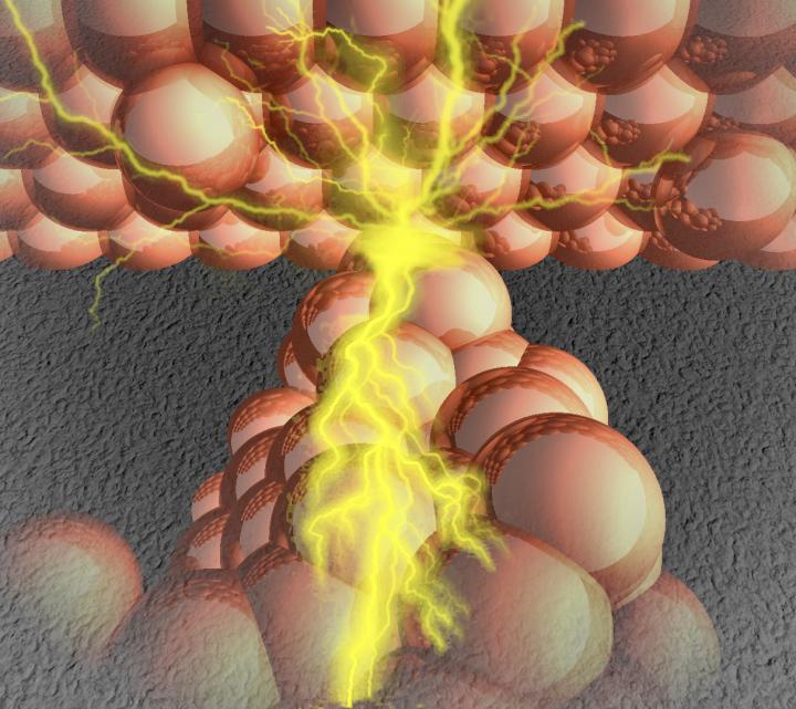
All of these things make this discovery easy to marvel at and somewhat impossible to picture. Luckily, artists have taken up the task of imagining it for us, which you’ve likely seen if you’ve already stumbled on coverage of the discovery. Two bright, furious spheres of light and gas spiraling quickly into one another, resulting in a massive swell of lit-up matter along with light and gravitational waves rippling off speedily in all directions, towards parts unknown. These illustrations aren’t just alluring interpretations of a rare phenomenon; they are, to some extent, the translation of raw data and numbers into a tangible visual that gives scientists and nonscientists alike some way of grasping what just happened. But are these visualizations realistic? Is this what it actually looked like? No one has any idea. Which is what makes the scientific illustrators’ work all the more fascinating.

“My goal is to represent what the scientists found,” says Aurore Simmonet, a scientific illustrator based at Sonoma State University in Rohnert Park, California. Even though she said she doesn’t have a rigorous science background (she certainly didn’t know what a kilonova was before being tasked to illustrate one), she also doesn’t believe that type of experience is an absolute necessity. More critical, she says, is for the artist to have an interest in the subject matter and in learning new things, as well as a capacity to speak directly to scientists about their work.

Illustrators like Simmonet usually start off work on an illustration by asking the scientist what’s the biggest takeaway a viewer should grasp when looking at a visual. Unfortunately, this latest discovery yielded a multitude of papers emphasizing different conclusions and highlights. With so many scientific angles, there’s a stark challenge in trying to cram every important thing into a single drawing.

Clearly, however, the illustrations needed to center around the kilonova. Simmonet loves colors, so she began by discussing with the researchers what kind of color scheme would work best. The smash of two neutron stars lends itself well to deep, vibrant hues. Simmonet and Robin Dienel at the Carnegie Institution for Science elected to use a wide array of colors and drew bright cracking to show pressure forming at the merging. Others, like Luis Calcada at the European Southern Observatory, limited the color scheme in favor of emphasizing the bright moment of collision and the signal waves created by the kilonova.

Animators have even more freedom to show the event, since they have much more than a single frame to play with. The Conceptual Image Lab at NASA’s [US National Aeronautics and Space Administration] Goddard Space Flight Center created a short video about the new findings, and lead animator Brian Monroe says the video he and his colleagues designed shows off the evolution of the entire process: the rising action, climax, and resolution of the kilonova event.

The illustrators try to adhere to what the likely physics of the event entailed, soliciting feedback from the scientists to make sure they’re getting it right. The swirling of gas, the direction of ejected matter upon impact, the reflection of light, the proportions of the objects—all of these things are deliberately framed such that they make scientific sense. …

Do take a look at Patel’s piece, if for no other reason than to see all of the images he has embedded there. You may recognize Aurore Simmonet’s name from the credit line in the second image I have embedded here.

Substituting graphene and other carbon materials for scarce metals

A Sept. 19, 2017 news item on Nanowerk announces a new paper from the Chalmers University of Technology (Sweden), the lead institution for the Graphene Flagship (a 1B Euro 10 year European Commission programme), Note: A link has been removed,

Scarce metals are found in a wide range of everyday objects around us. They are complicated to extract, difficult to recycle and so rare that several of them have become “conflict minerals” which can promote conflicts and oppression. A survey at Chalmers University of Technology now shows that there are potential technology-based solutions that can replace many of the metals with carbon nanomaterials, such as graphene (Journal of Cleaner Production, “Carbon nanomaterials as potential substitutes for scarce metals”).

They can be found in your computer, in your mobile phone, in almost all other electronic equipment and in many of the plastics around you. Society is highly dependent on scarce metals, and this dependence has many disadvantages.

A Sept. 19, 2017 Chalmers University of Technology press release by Ulrika Ernstrom,, which originated the news item, provides more detail about the possibilities,

They can be found in your computer, in your mobile phone, in many of the plastics around you and in almost all electronic equipment. Society is highly dependent on scarce metals, and this dependence has many disadvantages.
Scarce metals such as tin, silver, tungsten and indium are both rare and difficult to extract since the workable concentrations are very small. This ensures the metals are highly sought after – and their extraction is a breeding ground for conflicts, such as in the Democratic Republic of the Congo where they fund armed conflicts.
In addition, they are difficult to recycle profitably since they are often present in small quantities in various components such as electronics.
Rickard Arvidsson and Björn Sandén, researchers in environmental systems analysis at Chalmers University of Technology, have now examined an alternative solution: substituting carbon nanomaterials for the scarce metals. These substances – the best known of which is graphene – are strong materials with good conductivity, like scarce metals.
“Now technology development has allowed us to make greater use of the common element carbon,” says Sandén. “Today there are many new carbon nanomaterials with similar properties to metals. It’s a welcome new track, and it’s important to invest in both the recycling and substitution of scarce metalsfrom now on.”
The Chalmers researchers have studied  the main applications of 14 different metals, and by reviewing patents and scientific literature have investigated the potential for replacing them by carbon nanomaterials. The results provide a unique overview of research and technology development in the field.
According to Arvidsson and Sandén the summary shows that a shift away from the use of scarce metals to carbon nanomaterials is already taking place.
….
“There are potential technology-based solutions for replacing 13 out of the 14 metals by carbon nanomaterials in their most common applications. The technology development is at different stages for different metals and applications, but in some cases such as indium and gallium, the results are very promising,” Arvidsson says.
“This offers hope,” says Sandén. “In the debate on resource constraints, circular economy and society’s handling of materials, the focus has long been on recycling and reuse. Substitution is a potential alternative that has not been explored to the same extent and as the resource issues become more pressing, we now have more tools to work with.”
The research findings were recently published in the Journal of Cleaner Production. Arvidsson and Sandén stress that there are significant potential benefits from reducing the use of scarce metals, and they hope to be able to strengthen the case for more research and development in the field.
“Imagine being able to replace scarce metals with carbon,” Sandén says. “Extracting the carbon from biomass would create a natural cycle.”
“Since carbon is such a common and readily available material, it would also be possible to reduce the conflicts and geopolitical problems associated with these metals,” Arvidsson says.
At the same time they point out that more research is needed in the field in order to deal with any new problems that may arise if the scarce metals are replaced.
“Carbon nanomaterials are only a relatively recent discovery, and so far knowledge is limited about their environmental impact from a life-cycle perspective. But generally there seems to be a potential for a low environmental impact,” Arvidsson says.

FACTS AND MORE INFORMATION

Carbon nanomaterials consist solely or mainly of carbon, and are strong materials with good conductivity. Several scarce metals have similar properties. The metals are found, for example, in cables, thin screens, flame-retardants, corrosion protection and capacitors.
Rickard Arvidsson and Björn Sandén at Chalmers University of Technology have investigated whether the carbon nanomaterials graphene, fullerenes and carbon nanotubes have the potential to replace 14 scarce metals in their main areas of application (see table). They found potential technology-based solutions to replace the metals with carbon nanomaterials for all applications except for gold in jewellery. The metals which we are closest to being able to substitute are indium, gallium, beryllium and silver.

Here’s a link to and a citation for the paper,

Carbon nanomaterials as potential substitutes for scarce metals by Rickard Arvidsson, Björn A. Sandén. Journal of Cleaner Production (0959-6526). Vol. 156 (2017), p. 253-261. DOI: https://doi.org/10.1016/j.jclepro.2017.04.048

This paper appears to be open access.

Controlling the nanostructure of inorganic materials with tumor suppressor proteins

A May 3, 2017 news item on Nanowerk announces research from Japan on using tumor suppressor proteins to control nanostructures,

A new method combining tumor suppressor protein p53 and biomineralization peptide BMPep successfully created hexagonal silver nanoplates, suggesting an efficient strategy for controlling the nanostructure of inorganic materials.

Precise control of nanostructures is a key factor to form functional nanomaterials. Biomimetic approaches are considered effective for fabricating nanomaterials because biomolecules are able to bind with specific targets, self-assemble, and build complex structures. Oligomerization, or the assembly of biomolecules, is a crucial aspect of natural materials that form higher-ordered structures.

A May 3,2017 Hokkaido University research press release, which originated the news item, delves into the details,

Some peptides are known to bind with a specific inorganic substance, such as silver, and enhance its crystal formation. This phenomenon, called peptide-mediated biomineralization, could be used as a biomimetic approach to create functional inorganic structures. Controlling the spatial orientation of the peptides could yield complex inorganic structures, but this has long been a great challenge.

A team of researchers led by Hokkaido University Professor Kazuyasu Sakaguchi has succeeded in controlling the oligomerization of the silver biomineralization peptide (BMPep) which led to the creation of hexagonal silver nanoplates.

The team utilized the well-known tumor suppressor protein p53 which has been known to form tetramers through its tetramerization domain (p53Tet). “The unique symmetry of the p53 tetramer is an attractive scaffold to be used in controlling the overall oligomerization state of the silver BMPep such as its spatial orientation, geometry, and valency,” says Sakaguchi.

In the experiments, the team successfully created silver BMPep fused with p53Tet. This resulted in the formation of BMPep tetramers which yielded hexagonal silver nanoplates. They also found that the BMPep tetramers have enhanced specificity to the structured silver surface, apparently regulating the direction of crystal growth to form hexagonal nanoplates. Furthermore, the tetrameric peptide acted as a catalyst, controlling the silver’s crystal growth without consuming the peptide.

“Our novel method can be applied to other biomineralization peptides and oligomerization proteins, thus providing an efficient and versatile strategy for controlling nanostructures of various inorganic materials. The production of tailor-made nanomaterials is now more feasible,” Sakaguchi commented.

monomeric and tetrameric biomineralization peptides

(Left panels) Schematic illustrations of monomeric and tetrameric biomineralization peptides fused with p53Tet and electron microscopy images of silver nanostructures formed by the biomineralization peptides. Scale bar = 100 nm. (Right) The proposed model in which tetrameric biomineralization peptides regulate the direction of crystal growth and therefore its nanostructure.

Here’s a link to and a citation for the paper,

Oligomerization enhances the binding affinity of a silver biomineralization peptide and catalyzes nanostructure formation by Tatsuya Sakaguchi, Jose Isagani B. Janairo, Mathieu Lussier-Price, Junya Wada, James G. Omichinski, & Kazuyasu Sakaguchi. Scientific Reports 7, Article number: 1400 (2017)  doi:10.1038/s41598-017-01442-8 Published online: 03 May 2017

This paper is open access.

Is there a risk of resistance to nanosilver?

Anyone who’s noticed how popular silver has become as an antibacterial, antifungal, or antiviral agent may have wondered if resistance might occur as its use becomes more common. I have two bits on the topic, one from Australia and the other from Canada.

Australia

Researchers in Australia don’t have a definitive statement on the issue but are suggesting more caution (from a March 31, 2017 news item on Nanowerk),

Researchers at the University of Technology Sydney [UTS] warn that the broad-spectrum antimicrobial effectiveness of silver is being put at risk by the widespread and inappropriate expansion of nanosilver use in medical and consumer goods.

As well as their use in medical items such as wound dressings and catheters, silver nanoparticles are becoming ubiquitous in everyday items, including toothbrushes and toothpaste, baby bottles and teats, bedding, clothing and household appliances, because of their antibacterial potency and the incorrect assumption that ordinary items should be kept “clean” of microbes.

Nanobiologist Dr Cindy Gunawan, from the ithree institute at UTS and lead researcher on the investigation, said alarm bells should be ringing at the commercialisation of nanosilver use because of a “real threat” that resistance to nanosilver will develop and spread through microorganisms in the human body and the environment.

A March 31 (?), 2017 University of Technology Sydney press release by Fiona McGill, which originated the news item, expands on the theme,

Dr Gunawan and ithree institute director Professor Liz Harry, in collaboration with researchers at UNSW [University of New South Wales] and abroad, investigated more than 140 commercially available medical devices, including wound dressings and tracheal and urinary catheters, and dietary supplements, which are promoted as immunity boosters and consumed by throat or nasal spray.

Their perspective article in the journal ACS Nano concluded that the use of nanosilver in these items could lead to prolonged exposure to bioactive silver in the human body. Such exposure creates the conditions for microbial resistance to develop.

E. coli bacteria. Photo: Flickr/NIAID


The use of silver as an antimicrobial agent dates back centuries. Its ability to destroy pathogens while seemingly having low toxicity on human cells has seen it widely employed, in treating burns or purifying water, for example. More recently, ultra-small (less than 10,000th of a millimetre) silver nanoparticles have been engineered for antimicrobial purposes.  Their commercial appeal lies in superior potency at lower concentrations than “bulk” silver.

“Nanosilver is a proven antimicrobial agent whose reliability is being jeopardised by the commercialisation of people’s fear of bacteria,” Dr Gunawan said.

“Our use of it needs to be far more judicious, in the same way we need to approach antibiotic usage. Nanosilver is a useful tool but we need to be careful, use it wisely and only when the benefit outweighs the risk.

“People need to be made aware of just how widely it is used, but more importantly they need to be made aware that the presence of nanosilver has been shown to cause antimicrobial resistance.”

What is also needed, Dr Gunawan said, is a targeted surveillance strategy to monitor for any occurrence of resistance.

Professor Harry said the findings were a significant contribution to addressing the global antimicrobial resistance crisis.

“This research emphasises the threat posed to our health and that of the environment by the inappropriate use of nanosilver as an antibacterial, particularly in ordinary household and consumer items,” she said.

Here’s a link to and a citation for the paper,

Widespread and Indiscriminate Nanosilver Use: Genuine Potential for Microbial Resistance by Cindy Gunawan, Christopher P. Marquis, Rose Amal, Georgios A. Sotiriou, Scott A. Rice⊥, and Elizabeth J. Harry. ACS Nano, Article ASAP DOI: 10.1021/acsnano.7b01166 Publication Date (Web): March 24, 2017

Copyright © 2017 American Chemical Society

This paper is behind a paywall.

Meanwhile, researchers at the University Calgary (Alberta, Canada) may have discovered what could cause resistance to silver.

Canada

This April 25, 2017 news release on EurekAlert is from the Experimental Biology Annual Meeting 2017,

Silver and other metals have been used to fight infections since ancient times. Today, researchers are using sophisticated techniques such as the gene-editing platform Crispr-Cas9 to take a closer look at precisely how silver poisons pathogenic microbes–and when it fails. The work is yielding new insights on how to create effective antimicrobials and avoid the pitfalls of antimicrobial resistance.

Joe Lemire, a postdoctoral fellow at the University of Calgary, will present his work in this area at the American Society for Biochemistry and Molecular Biology annual meeting during the Experimental Biology 2017 meeting, to be held April 22-26 in Chicago.

“Our overarching goal is to deliver the relevant scientific evidence that would aid policymakers in developing guidelines for when and how silver could be used in the clinic to combat and control infectious pathogens,” said Lemire. “With our enhanced mechanistic understanding of silver toxicity, we also aim to develop novel silver-based antimicrobial therapies, and potentially rejuvenate other antibiotic therapies that bacteria have come to resist, via silver-based co-treatment strategies.”

Lemire and his colleagues are using Crispr-Cas9 genome editing to screen for and delete genes that allow certain bacterial species to resist silver’s antimicrobial properties. [emphasis mine] Although previous methods allowed researchers to identify genes that confer antibiotic resistance or tolerance, Crispr-Cas9 is the first technology to allow researchers to cleanly delete these genes from the genome without leaving behind any biochemical markers or “scars.”

The team has discovered many biological pathways involved in silver toxicity and some surprising ways that bacteria avoid succumbing to silver poisoning, Lemire said. While silver is used to control bacteria in many clinical settings and has been incorporated into hundreds of commercial products, gaining a more complete understanding of silver’s antimicrobial properties is necessary if we are to make the most of this ancient remedy for years to come.

###

Joe Lemire will present this research at 12-2:30 p.m. Tuesday, April 25, [2017] in Hall F, McCormick Place Convention Center (poster B379 939.2) (abstract). Contact the media team for more information or to obtain a free press pass to attend the meeting.

About Experimental Biology 2017

Experimental Biology is an annual meeting comprised of more than 14,000 scientists and exhibitors from six host societies and multiple guest societies. With a mission to share the newest scientific concepts and research findings shaping clinical advances, the meeting offers an unparalleled opportunity for exchange among scientists from across the U.S. and the world who represent dozens of scientific areas, from laboratory to translational to clinical research. http://www.experimentalbiology.org #expbio

About the American Society for Biochemistry and Molecular Biology (ASBMB)

ASBMB is a nonprofit scientific and educational organization with more than 12,000 members worldwide. Founded in 1906 to advance the science of biochemistry and molecular biology, the society publishes three peer-reviewed journals, advocates for funding of basic research and education, supports science education at all levels, and promotes the diversity of individuals entering the scientific workforce. http://www.asbmb.org

Lemire’s co-authors for the work presented at the 2017 annual meeting are: Kate Chatfield-Reed (The University of Calgary), Lindsay Kalan (Perelman School of Medicine), Natalie Gugala (The University of Calgary), Connor Westersund (The University of Calgary), Henrik Almblad (The University of Calgary), Gordon Chua (The University of Calgary), Raymond Turner (The University of Calgary).

For anyone who wants to pursue this research a little further, the most recent paper I can find is this one from 2015,

Silver oxynitrate: An Unexplored Silver Compound with Antimicrobial and Antibiofilm Activity by Joe A. Lemire, Lindsay Kalan, Alexandru Bradu, and Raymond J. Turner. Antimicrobial Agents and Chemotherapy 05177-14, doi: 10.1128/AAC.05177-14 Accepted manuscript posted online 27 April 2015

This paper appears to be open access.

Transparent silver

This March 21, 2017 news item on Nanowerk is the first I’ve heard of transparent silver; it’s usually transparent aluminum (Note: A link has been removed),

The thinnest, smoothest layer of silver that can survive air exposure has been laid down at the University of Michigan, and it could change the way touchscreens and flat or flexible displays are made (Advanced Materials, “High-performance Doped Silver Films: Overcoming Fundamental Material Limits for Nanophotonic Applications”).

It could also help improve computing power, affecting both the transfer of information within a silicon chip and the patterning of the chip itself through metamaterial superlenses.

A March 21, 2017 University of Michigan  news release, which originated the news item, provides details about the research and features a mention about aluminum,

By combining the silver with a little bit of aluminum, the U-M researchers found that it was possible to produce exceptionally thin, smooth layers of silver that are resistant to tarnishing. They applied an anti-reflective coating to make one thin metal layer up to 92.4 percent transparent.

The team showed that the silver coating could guide light about 10 times as far as other metal waveguides—a property that could make it useful for faster computing. And they layered the silver films into a metamaterial hyperlens that could be used to create dense patterns with feature sizes a fraction of what is possible with ordinary ultraviolet methods, on silicon chips, for instance.

Screens of all stripes need transparent electrodes to control which pixels are lit up, but touchscreens are particularly dependent on them. A modern touch screen is made of a transparent conductive layer covered with a nonconductive layer. It senses electrical changes where a conductive object—such as a finger—is pressed against the screen.

“The transparent conductor market has been dominated to this day by one single material,” said L. Jay Guo, professor of electrical engineering and computer science.

This material, indium tin oxide, is projected to become expensive as demand for touch screens continues to grow; there are relatively few known sources of indium, Guo said.

“Before, it was very cheap. Now, the price is rising sharply,” he said.

The ultrathin film could make silver a worthy successor.

Usually, it’s impossible to make a continuous layer of silver less than 15 nanometers thick, or roughly 100 silver atoms. Silver has a tendency to cluster together in small islands rather than extend into an even coating, Guo said.

By adding about 6 percent aluminum, the researchers coaxed the metal into a film of less than half that thickness—seven nanometers. What’s more, when they exposed it to air, it didn’t immediately tarnish as pure silver films do. After several months, the film maintained its conductive properties and transparency. And it was firmly stuck on, whereas pure silver comes off glass with Scotch tape.

In addition to their potential to serve as transparent conductors for touch screens, the thin silver films offer two more tricks, both having to do with silver’s unparalleled ability to transport visible and infrared light waves along its surface. The light waves shrink and travel as so-called surface plasmon polaritons, showing up as oscillations in the concentration of electrons on the silver’s surface.

Those oscillations encode the frequency of the light, preserving it so that it can emerge on the other side. While optical fibers can’t scale down to the size of copper wires on today’s computer chips, plasmonic waveguides could allow information to travel in optical rather than electronic form for faster data transfer. As a waveguide, the smooth silver film could transport the surface plasmons over a centimeter—enough to get by inside a computer chip.

Here’s a link to and a citation for the paper,

High-Performance Doped Silver Films: Overcoming Fundamental Material Limits for Nanophotonic Applications by Cheng Zhang, Nathaniel Kinsey, Long Chen, Chengang Ji, Mingjie Xu, Marcello Ferrera, Xiaoqing Pan, Vladimir M. Shalaev, Alexandra Boltasseva, and Jay Guo. Advanced Materials DOI: 10.1002/adma.201605177 Version of Record online: 20 MAR 2017

© 2017 WILEY-VCH Verlag GmbH & Co. KGaA, Weinheim

This paper is behind a paywall.

Plasmonic ‘Goldfinger’: antifungal nail polish with metallic nanoparticles

A March 29,.2017 news item on Nanowerk announces a new kind of nanopolish,

Since ancient times, people have used lustrous silver, platinum and gold to make jewelry and other adornments. Researchers have now developed a new way to add the metals to nail polish with minimal additives, resulting in durable, tinted — and potentially antibacterial — nail coloring.

Using metal nanoparticles in clear nail polish makes it durable and colorful without extra additives.
Credit: American Chemical Society

A March 29, 2017 American Chemical Society (ACS) news release (also on EurekAlert), which originated the news item, adds a little more detail (Note: A link has been removed),

Nail polish comes in a bewildering array of colors. Current coloring techniques commonly incorporate pigment powders and additives. Scientists have recently started exploring the use of nanoparticles in polishes and have found that they can improve their durability and, in the case of silver nanoparticles, can treat fungal toenail infections. Marcus Lau, Friedrich Waag and Stephan Barcikowski wanted to see if they could come up with a simple way to integrate metal nanoparticles in nail polish.

The researchers started with store-bought bottles of clear, colorless nail polish and added small pieces of silver, gold, platinum or an alloy to them. To break the metals into nanoparticles, they shone a laser on them in short bursts over 15 minutes. Analysis showed that the method resulted in a variety of colored, transparent polishes with a metallic sheen. The researchers also used laser ablation to produce a master batch of metal nanoparticles in ethyl acetate, a polish thinner, which could then be added to individual bottles of polish. This could help boost the amount of production for commercialization. The researchers say the technique could also be used to create coatings for medical devices.

The authors acknowledge funding from the INTERREG-Program Germany-Netherlands.

A transparent nail varnish can be colored simply and directly with laser-generated nanoparticles. This does not only enable coloring of the varnish for cosmetic purposes, but also gives direct access to nanodoped varnishes to be used on any solid surface. Therefore, nanoparticle properties such as plasmonic properties or antibacterial effects can be easily adapted to surfaces for medical or optical purposes. The presented method for integration of metal (gold, platinum, silver, and alloy) nanoparticles into varnishes is straightforward and gives access to nanodoped polishes with optical properties, difficult to be achieved by dispersing powder pigments in the high-viscosity liquids. Courtesy: Industrial and Engineering & Chemistry Research

Here’s a link to and a citation for the paper,

Direct Integration of Laser-Generated Nanoparticles into Transparent Nail Polish: The Plasmonic “Goldfinger” by Marcus Lau, Friedrich Waag, and Stephan Barcikowski. Ind. Eng. Chem. Res., 2017, 56 (12), pp 3291–3296 DOI: 10.1021/acs.iecr.7b00039 Publication Date (Web): March 7, 2017

Copyright © 2017 American Chemical Society

This paper is behind a paywall.