Tag Archives: silicon nanowires

A solar, self-charging supercapacitor for wearable technology

Ravinder Dahiya, Carlos García Núñez, and their colleagues at the University of Glasgow (Scotland) strike again (see my May 10, 2017 posting for their first ‘solar-powered graphene skin’ research announcement). Last time it was all about robots and prosthetics, this time they’ve focused on wearable technology according to a July 18, 2018 news item on phys.org,

A new form of solar-powered supercapacitor could help make future wearable technologies lighter and more energy-efficient, scientists say.

In a paper published in the journal Nano Energy, researchers from the University of Glasgow’s Bendable Electronics and Sensing Technologies (BEST) group describe how they have developed a promising new type of graphene supercapacitor, which could be used in the next generation of wearable health sensors.

A July 18, 2018 University of Glasgow press release, which originated the news item, explains further,

Currently, wearable systems generally rely on relatively heavy, inflexible batteries, which can be uncomfortable for long-term users. The BEST team, led by Professor Ravinder Dahiya, have built on their previous success in developing flexible sensors by developing a supercapacitor which could power health sensors capable of conforming to wearer’s bodies, offering more comfort and a more consistent contact with skin to better collect health data.

Their new supercapacitor uses layers of flexible, three-dimensional porous foam formed from graphene and silver to produce a device capable of storing and releasing around three times more power than any similar flexible supercapacitor. The team demonstrated the durability of the supercapacitor, showing that it provided power consistently across 25,000 charging and discharging cycles.

They have also found a way to charge the system by integrating it with flexible solar powered skin already developed by the BEST group, effectively creating an entirely self-charging system, as well as a pH sensor which uses wearer’s sweat to monitor their health.

Professor Dahiya said: “We’re very pleased by the progress this new form of solar-powered supercapacitor represents. A flexible, wearable health monitoring system which only requires exposure to sunlight to charge has a lot of obvious commercial appeal, but the underlying technology has a great deal of additional potential.

“This research could take the wearable systems for health monitoring to remote parts of the world where solar power is often the most reliable source of energy, and it could also increase the efficiency of hybrid electric vehicles. We’re already looking at further integrating the technology into flexible synthetic skin which we’re developing for use in advanced prosthetics.” [emphasis mine]

In addition to the team’s work on robots, prosthetics, and graphene ‘skin’ mentioned in the May 10, 2017 posting the team is working on a synthetic ‘brainy’ skin for which they have just received £1.5m funding from the Engineering and Physical Science Research Council (EPSRC).

Brainy skin

A July 3, 2018 University of Glasgow press release discusses the proposed work in more detail,

A robotic hand covered in ‘brainy skin’ that mimics the human sense of touch is being developed by scientists.

University of Glasgow’s Professor Ravinder Dahiya has plans to develop ultra-flexible, synthetic Brainy Skin that ‘thinks for itself’.

The super-flexible, hypersensitive skin may one day be used to make more responsive prosthetics for amputees, or to build robots with a sense of touch.

Brainy Skin reacts like human skin, which has its own neurons that respond immediately to touch rather than having to relay the whole message to the brain.

This electronic ‘thinking skin’ is made from silicon based printed neural transistors and graphene – an ultra-thin form of carbon that is only an atom thick, but stronger than steel.

The new version is more powerful, less cumbersome and would work better than earlier prototypes, also developed by Professor Dahiya and his Bendable Electronics and Sensing Technologies (BEST) team at the University’s School of Engineering.

His futuristic research, called neuPRINTSKIN (Neuromorphic Printed Tactile Skin), has just received another £1.5m funding from the Engineering and Physical Science Research Council (EPSRC).

Professor Dahiya said: “Human skin is an incredibly complex system capable of detecting pressure, temperature and texture through an array of neural sensors that carry signals from the skin to the brain.

“Inspired by real skin, this project will harness the technological advances in electronic engineering to mimic some features of human skin, such as softness, bendability and now, also sense of touch. This skin will not just mimic the morphology of the skin but also its functionality.

“Brainy Skin is critical for the autonomy of robots and for a safe human-robot interaction to meet emerging societal needs such as helping the elderly.”
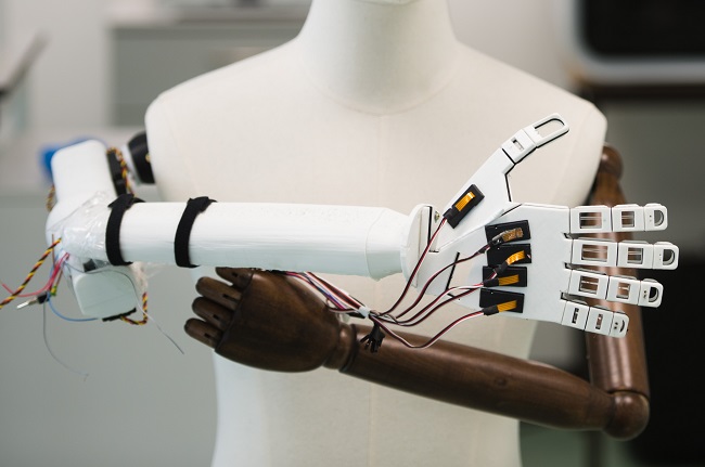
Synthetic ‘Brainy Skin’ with sense of touch gets £1.5m funding. Photo of Professor Ravinder Dahiya

This latest advance means tactile data is gathered over large areas by the synthetic skin’s computing system rather than sent to the brain for interpretation.

With additional EPSRC funding, which extends Professor Dahiya’s fellowship by another three years, he plans to introduce tactile skin with neuron-like processing. This breakthrough in the tactile sensing research will lead to the first neuromorphic tactile skin, or ‘brainy skin.’

To achieve this, Professor Dahiya will add a new neural layer to the e-skin that he has already developed using printing silicon nanowires.

Professor Dahiya added: “By adding a neural layer underneath the current tactile skin, neuPRINTSKIN will add significant new perspective to the e-skin research, and trigger transformations in several areas such as robotics, prosthetics, artificial intelligence, wearable systems, next-generation computing, and flexible and printed electronics.”

The Engineering and Physical Sciences Research Council (EPSRC) is part of UK Research and Innovation, a non-departmental public body funded by a grant-in-aid from the UK government.

EPSRC is the main funding body for engineering and physical sciences research in the UK. By investing in research and postgraduate training, the EPSRC is building the knowledge and skills base needed to address the scientific and technological challenges facing the nation.

Its portfolio covers a vast range of fields from healthcare technologies to structural engineering, manufacturing to mathematics, advanced materials to chemistry. The research funded by EPSRC has impact across all sectors. It provides a platform for future UK prosperity by contributing to a healthy, connected, resilient, productive nation.

It’s fascinating to note how these pieces of research fit together for wearable technology and health monitoring and creating more responsive robot ‘skin’ and, possibly, prosthetic devices that would allow someone to feel again.

The latest research paper

Getting back the solar-charging supercapacitors mentioned in the opening, here’s a link to and a citation for the team’s latest research paper,

Flexible self-charging supercapacitor based on graphene-Ag-3D graphene foam electrodes by Libu Manjakka, Carlos García Núñez, Wenting Dang, Ravinder Dahiya. Nano Energy Volume 51, September 2018, Pages 604-612 DOI: https://doi.org/10.1016/j.nanoen.2018.06.072

This paper is open access.
Taking spectroscopy to a new dimension with silver nanoparticles

This latest move towards better detection at the nanoscale comes from India (from a January 2, 2018 news item on ScienceDaily),

As medicine and pharmacology investigate nanoscale processes, it has become increasingly important to identify and characterize different molecules. Raman spectroscopy, a technique that leverages the scattering of laser light to identify molecules, has a limited capacity to detect molecules in diluted samples because of low signal yield.

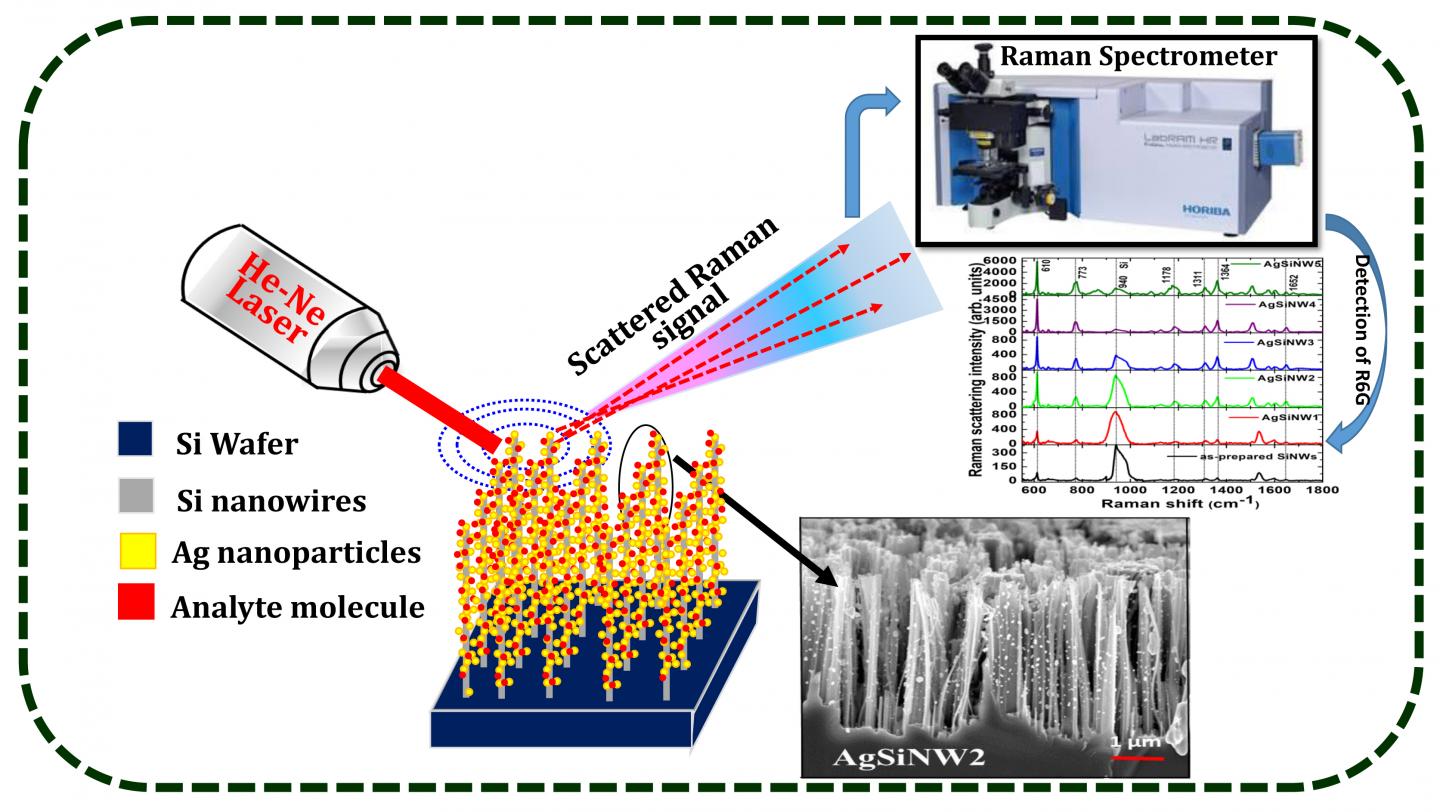
A team of researchers from the University of Hyderabad in India has improved molecular detection at low concentration levels by arranging nanoparticles on nanowires to enhance Raman spectroscopy. Surface-enhanced Raman spectroscopy (SERS) uses electromagnetic fields to improve Raman scattering and boost sensitivity in standard dyes such as R6G by more than one billionfold.

Here’s an image illustrating the work,

Caption: Detection of a low concentration analyte molecule using silicon nanowires decorated with silver nanoparticles and surface enhanced Raman scattering measurements. Credit: V.S. Vendamani

A January 2, 2017 American Institute of Physics press release on EurekAlert, which originated the news item, explains further,

The team decorated vertically aligned silicon nanowires with varying densities of silver nanoparticles, utilizing and enhancing the structure’s 3-D shape. Their results, published in the Journal of Applied Physics, from AIP [American Institute of Physics] Publishing, show that their device was able to enhance the Raman signals for cytosine protein and ammonium perchlorate by a factor of 100,000.

“The beauty is that we can improve the density of these nanowires using simple chemistry,” said Soma Venugopal Rao, one of the paper’s authors. “If you have a large density of nanowires, you can put more silver nanoparticles into the substrate and can increase the sensitivity of the substrate.”

Applying the necessary nanostructures to SERS devices remains a challenge for the field. Building these structures in three dimensions with silicon nanowires has garnered attention for their higher surface area and superior performance, but silicon nanowires are still expensive to produce.

Instead, the team was able to find a cheaper way to make silicon nanowires and used a technique called electroless etching to make a wide range of nanowires. They “decorated” these wires with silver nanoparticles with variable and controlled densities, which increased the nanowires’ surface area.

“Optimizing these vertically aligned structures took a lot of time in the beginning,” said Nageswara Rao, another of the paper’s authors. “We increased the surface area and to do this we needed to change the aspect ratio.”

After optimizing their system to detect Rhodamine dye on a nanomolar level, these new substrates the team built enhanced Raman sensitivity by a factor of 10,000 to 100,000. The substrates detected concentrations of cytosine, a nucleotide found in DNA, and ammonium perchlorate, a molecule with potential for detecting explosives, in as dilute concentrations as 50 and 10 micromolar, respectively.

The results have given the team reason to believe that it might soon be possible to detect compounds in concentrations on the scale of nanomolar or even picomolar, Nageswara Rao said. The team’s work has opened several avenues for future research, from experimenting with different nanoparticles such as gold, increasing the sharpness of the nanowires or testing these devices across several types of molecules.

Here’s a link to and a citation for the paper,

Three-dimensional hybrid silicon nanostructures for surface enhanced Raman spectroscopy based molecular detection featured by V. S. Vendamani, S. V. S. Nageswara Rao, S. Venugopal Rao, D. Kanjilal, and A. P. Pathak. Journal of Applied Physics 123, 014301 (2018); Published Online: January 2018 https://doi.org/10.1063/1.5000994

This paper is open access.

A new class of artificial retina

If I read the news release rightly (keep scrolling), this particular artificial retina does not require a device outside the body (e.g. specially developed eyeglasses) to capture an image to be transmitted to the implant. This new artificial retina captures the image directly.

The announcement of a new artificial retina is made in a March 13, 2017 news item on Nanowerk (Note: A link has been removed),

A team of engineers at the University of California San Diego and La Jolla-based startup Nanovision Biosciences Inc. have developed the nanotechnology and wireless electronics for a new type of retinal prosthesis that brings research a step closer to restoring the ability of neurons in the retina to respond to light. The researchers demonstrated this response to light in a rat retina interfacing with a prototype of the device in vitro.

They detail their work in a recent issue of the Journal of Neural Engineering (“Towards high-resolution retinal prostheses with direct optical addressing and inductive telemetry”). The technology could help tens of millions of people worldwide suffering from neurodegenerative diseases that affect eyesight, including macular degeneration, retinitis pigmentosa and loss of vision due to diabetes

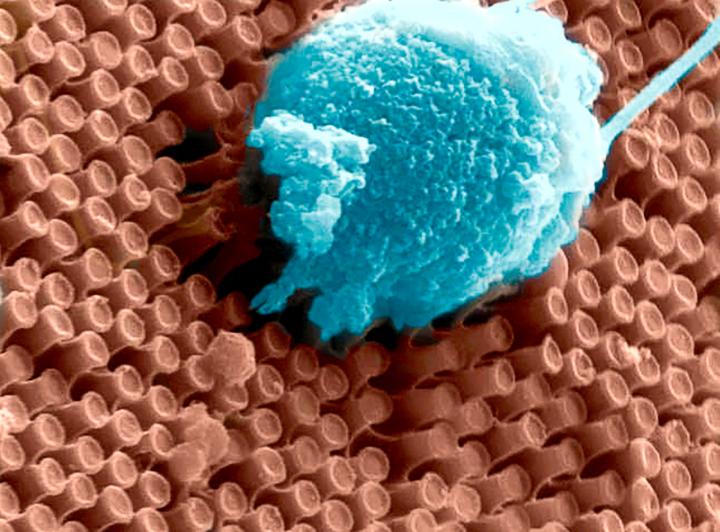
Caption: These are primary cortical neurons cultured on the surface of an array of optoelectronic nanowires. Here a neuron is pulling the nanowires, indicating the the cell is doing well on this material. Credit: UC San Diego

A March 13, 2017 University of California at San Diego (UCSD) news release (also on EurekAlert) by Ioana Patringenaru, which originated the news item, details the new approach,

Despite tremendous advances in the development of retinal prostheses over the past two decades, the performance of devices currently on the market to help the blind regain functional vision is still severely limited–well under the acuity threshold of 20/200 that defines legal blindness.

“We want to create a new class of devices with drastically improved capabilities to help people with impaired vision,” said Gabriel A. Silva, one of the senior authors of the work and professor in bioengineering and ophthalmology at UC San Diego. Silva also is one of the original founders of Nanovision.

The new prosthesis relies on two groundbreaking technologies. One consists of arrays of silicon nanowires that simultaneously sense light and electrically stimulate the retina accordingly. The nanowires give the prosthesis higher resolution than anything achieved by other devices–closer to the dense spacing of photoreceptors in the human retina. The other breakthrough is a wireless device that can transmit power and data to the nanowires over the same wireless link at record speed and energy efficiency.

One of the main differences between the researchers’ prototype and existing retinal prostheses is that the new system does not require a vision sensor outside of the eye [emphasis mine] to capture a visual scene and then transform it into alternating signals to sequentially stimulate retinal neurons. Instead, the silicon nanowires mimic the retina’s light-sensing cones and rods to directly stimulate retinal cells. Nanowires are bundled into a grid of electrodes, directly activated by light and powered by a single wireless electrical signal. This direct and local translation of incident light into electrical stimulation makes for a much simpler–and scalable–architecture for the prosthesis.

The power provided to the nanowires from the single wireless electrical signal gives the light-activated electrodes their high sensitivity while also controlling the timing of stimulation.

“To restore functional vision, it is critical that the neural interface matches the resolution and sensitivity of the human retina,” said Gert Cauwenberghs, a professor of bioengineering at the Jacobs School of Engineering at UC San Diego and the paper’s senior author.

Wireless telemetry system

Power is delivered wirelessly, from outside the body to the implant, through an inductive powering telemetry system developed by a team led by Cauwenberghs.

The device is highly energy efficient because it minimizes energy losses in wireless power and data transmission and in the stimulation process, recycling electrostatic energy circulating within the inductive resonant tank, and between capacitance on the electrodes and the resonant tank. Up to 90 percent of the energy transmitted is actually delivered and used for stimulation, which means less RF wireless power emitting radiation in the transmission, and less heating of the surrounding tissue from dissipated power.

The telemetry system is capable of transmitting both power and data over a single pair of inductive coils, one emitting from outside the body, and another on the receiving side in the eye. The link can send and receive one bit of data for every two cycles of the 13.56 megahertz RF signal; other two-coil systems need at least 5 cycles for every bit transmitted.

Proof-of-concept test

For proof-of-concept, the researchers inserted the wirelessly powered nanowire array beneath a transgenic rat retina with rhodopsin P23H knock-in retinal degeneration. The degenerated retina interfaced in vitro with a microelectrode array for recording extracellular neural action potentials (electrical “spikes” from neural activity).

The horizontal and bipolar neurons fired action potentials preferentially when the prosthesis was exposed to a combination of light and electrical potential–and were silent when either light or electrical bias was absent, confirming the light-activated and voltage-controlled responsivity of the nanowire array.

The wireless nanowire array device is the result of a collaboration between a multidisciplinary team led by Cauwenberghs, Silva and William R. Freeman, director of the Jacobs Retina Center at UC San Diego, UC San Diego electrical engineering professor Yu-Hwa Lo and Nanovision Biosciences.

A path to clinical translation

Freeman, Silva and Scott Thorogood, have co-founded La Jolla-based Nanovision Biosciences, a partner in this study, to further develop and translate the technology into clinical use, with the goal of restoring functional vision in patients with severe retinal degeneration. Animal tests with the device are in progress, with clinical trials following.

“We have made rapid progress with the development of the world’s first nanoengineered retinal prosthesis as a result of the unique partnership we have developed with the team at UC San Diego,” said Thorogood, who is the CEO of Nanovision Biosciences.

Here’s a link to and a citation for the paper,

Towards high-resolution retinal prostheses with direct optical addressing and inductive telemetry by Sohmyung Ha, Massoud L Khraiche, Abraham Akinin, Yi Jing, Samir Damle, Yanjin Kuang, Sue Bauchner, Yu-Hwa Lo, William R Freeman, Gabriel A Silva.Journal of Neural Engineering, Volume 13, Number 5 DOI: https://doi.org/10.1088/1741-2560/13/5/056008

Published 16 August 2016 • © 2016 IOP Publishing Ltd

I’m not sure why they waited so long to make the announcement but, in any event, this paper is behind a paywall.

Phagocytosis for a bioelectronic future

The process by which a cell engulfs matter is known as phagocytosis. One of the best known examples of failed phagocytosis is that of asbestos fibres in the lungs where lung cells have attempted to engulf a fibre that’s just too big and ends up piercing the cell. When enough of the cells are pierced, the person is diagnosed with mesothelioma.

This particular example of phagocytosis is a happier one according to a Dec. 16, 2016 article by Meghan Rosen for ScienceNews,

Human cells can snack on silicon.

Cells grown in the lab devour nano-sized wires of silicon through an engulfing process known as phagocytosis, scientists report December 16 in Science Advances.

Silicon-infused cells could merge electronics with biology, says John Zimmerman, a biophysicist now at Harvard University. “It’s still very early days,” he adds, but “the idea is to get traditional electronic devices working inside of cells.” Such hybrid devices could one day help control cellular behavior, or even replace electronics used for deep brain stimulation, he says.

Scientists have been trying to load electronic parts inside cells for years. One way is to zap holes in cells with electricity, which lets big stuff, like silicon nanowires linked to bulky materials, slip in. Zimmerman, then at the University of Chicago, and colleagues were looking for a simpler technique, something that would let tiny nanowires in easily and could potentially allow them to travel through a person’s bloodstream — like a drug.

A Dec. 22, 2016 University of Chicago news release by Matt Wood provides more detail,

“You can treat it as a non-genetic, synthetic biology platform,” said Bozhi Tian, PhD, assistant professor of chemistry and senior author of the new study. “Traditionally in biology we use genetic engineering and modify genetic parts. Now we can use silicon parts, and silicon can be internalized. You can target those silicon parts to specific parts of the cell and modulate that behavior with light.”

In the new study, Tian and his team show how cells consume or internalize the nanowires through phagocytosis, the same process they use to engulf and ingest nutrients and other particles in their environment. The nanowires are simply added to cell media, the liquid solution the cells live in, the same way you might administer a drug, and the cells take it from there. Eventually, the goal would be to inject them into the bloodstream or package them into a pill.

Once inside, the nanowires can interact directly with individual parts of the cell, organelles like the mitochondria, nucleus and cytoskeletal filaments. Researchers can then stimulate the nanowires with light to see how individual components of the cell respond, or even change the behavior of the cell. They can last up to two weeks inside the cell before biodegrading.

Seeing how individual parts of a cell respond to stimulation could give researchers insight into how medical treatments that use electrical stimulation work at a more detailed level. For instance, deep brain stimulation helps treat tremors from movement disorders like Parkinson’s disease by sending electrical signals to areas of the brain. Doctors know it works at the level of tissues and brain structures, but seeing how individual components of nerve cells react to these signals could help fine tune and improve the treatment.

The experiments in the study used umbilical vascular endothelial cells, which make up blood vessel linings in the umbilical cord. These cells readily took up the nanowires, but others, like cardiac muscle cells, did not. Knowing that some cells consume the wires and some don’t could also prove useful in experimental settings and give researchers more ways to target specific cell types.

Tian and his team manufactures the nanowires in their lab with a chemical vapor deposition system that grows the silicon structures to different specifications. They can adjust size, shape, and electrical properties as needed, or even add defects on purpose for testing. They can also make wires with porous surfaces that could deliver drugs or genetic material to the cells. The process gives them a variety of ways to manipulate the properties of the nanowires for research.

Here’s a link to and a citation for the paper,

Cellular uptake and dynamics of unlabeled freestanding silicon nanowires by John F. Zimmerman, Ramya Parameswaran, Graeme Murray, Yucai Wang, Michael Burke, and Bozhi Tian. Science Advances  16 Dec 2016: Vol. 2, no. 12, e1601039 DOI: 10.1126/sciadv.1601039

This paper appears to be open access.

Making nanoelectronic devices last longer in the body could lead to ‘cyborg’ tissue

An American Chemical Society (ACS) Feb. 19, 2014 news release (also on EurekAlert), describes some research devoted to extending a nanoelectronic device’s ‘life’ when implanted in the body,

The debut of cyborgs who are part human and part machine may be a long way off, but researchers say they now may be getting closer. In a study published in ACS’ journal Nano Letters, they report development of a coating that makes nanoelectronics much more stable in conditions mimicking those in the human body. [emphases mine] The advance could also aid in the development of very small implanted medical devices for monitoring health and disease.

Charles Lieber and colleagues note that nanoelectronic devices with nanowire components have unique abilities to probe and interface with living cells. They are much smaller than most implanted medical devices used today. For example, a pacemaker that regulates the heart is the size of a U.S. 50-cent coin, but nanoelectronics are so small that several hundred such devices would fit in the period at the end of this sentence. Laboratory versions made of silicon nanowires can detect disease biomarkers and even single virus cells, or record heart cells as they beat. Lieber’s team also has integrated nanoelectronics into living tissues in three dimensions — creating a “cyborg tissue.” One obstacle to the practical, long-term use of these devices is that they typically fall apart within weeks or days when implanted. In the current study, the researchers set out to make them much more stable.

They found that coating silicon nanowires with a metal oxide shell allowed nanowire devices to last for several months. This was in conditions that mimicked the temperature and composition of the inside of the human body. In preliminary studies, one shell material appears to extend the lifespan of nanoelectronics to about two years.

Depending on how you define the term cyborg, it could be said there are already cyborgs amongst us as I noted in an April 20, 2012 posting titled: My mother is a cyborg. Personally I’m fascinated by the news release’s mention of ‘cyborg tissue’ although there’s no further explanation of what the term might mean.

For the curious, here’s a link to and a citation for the paper,

Long Term Stability of Nanowire Nanoelectronics in Physiological Environments by Wei Zhou, Xiaochuan Dai, Tian-Ming Fu, Chong Xie, Jia Liu, and Charles M. Lieber. Nano Lett., Article ASAP DOI: 10.1021/nl500070h Publication Date (Web): January 30, 2014
Copyright © 2014 American Chemical Society

This paper is behind a paywall.