A July 19, 2019 news item on phys.org describes research that may result in a substantive change for information technology,
A team of researchers from Tokyo Institute of Technology has gained unprecedented insight into the inner workings of an atomic switch. By investigating the composition of the tiny metal ‘bridge’ that forms inside the switch, their findings may spur the design of atomic switches with improved performance.
A July 22, 2019 Tokyo Institute of Technology press release (also on EurekAlert but published July 19, 2019), which originated the news item, explains how this research could have such an important impact,
Atomic switches are hailed as the tiniest of electrochemical switches that could change the face of information technology. Due to their nanoscale dimensions and low power consumption, they hold promise for integration into next-generation circuits that could drive the development of artificial intelligence (AI) and Internet of Things (IoT) devices.
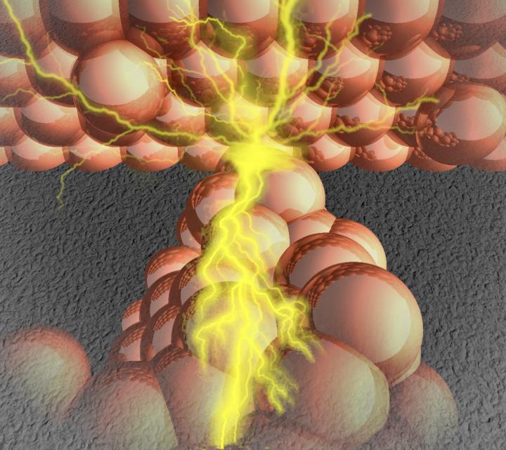
Although various designs have emerged, one intriguing question concerns the nature of the metallic filament, or bridge, that is key to the operation of the switch. The bridge forms inside a metal sulfide layer sandwiched between two electrodes [see figure below], and is controlled by applying a voltage that induces an electrochemical reaction. The formation and annihilation of this bridge determines whether the switch is on or off.
Now, a research group including Akira Aiba and Manabu Kiguchi and colleagues at Tokyo Institute of Technology’s Department of Chemistry has found a useful way to examine precisely what the bridge is composed of.
By cooling the atomic switch enough so as to be able to investigate the bridge using a low-temperature measurement technique called point contact spectroscopy (PCS) [2], their study revealed that the bridge is made up of metal atoms from both the electrode and the metal sulfide layer. This surprising finding controverts the prevailing notion that the bridge derives from the electrode only, Kiguchi explains.
The team compared atomic switches with different combinations of electrodes (Pt and Ag, or Pt and Cu) and metal sulfide layers (Cu2S and Ag2S). In both cases, they found that the bridge is mainly composed of Ag.
The reason behind the dominance of Ag in the bridge is likely due to “the higher mobility of Ag ions compared to Cu ions”, the researchers say in their paper published in ACS Applied Materials & Interfaces.
They conclude that “it would be better to use metals with low mobility” for designing atomic switches with higher stability.
Much remains to be explored in the advancement of atomic switch technologies, and the team is continuing to investigate which combination of elements would be the most effective in improving performance.
###
Technical terms
[1] Atomic switch: The idea behind an atomic switch — one that can be controlled by the motion of a single atom — was introduced by Donald Eigler and colleagues at the IBM Almaden Research Center in 1991. Interest has since focused on how to realize and harness the potential of such extremely small switches for use in logic circuits and memory devices. Over the past two decades, researchers in Japan have taken a world-leading role in the development of atomic switch technologies.
[2] Point contact spectroscopy: A method of measuring the properties or excitations of single atoms at low temperature.
Here’s a link to and a citation for the paper,
Investigation of Ag and Cu Filament Formation Inside the Metal Sulfide Layer of an Atomic Switch Based on Point-Contact Spectroscopy by A. Aiba, R. Koizumi, T. Tsuruoka, K. Terabe, K. Tsukagoshi, S. Kaneko, S. Fujii, T. Nishino, M. Kiguchi. ACS Appl. Mater. Interfaces 2019 XXXXXXXXXX-XXX DOI: https://doi.org/10.1021/acsami.9b05523 Publication Date:July 5, 2019 Copyright © 2019 American Chemical Society
This paper is behind a paywall.
For anyone who might need a bit of a refresher for the chemical elements, Pt is platinum, Ag is silver, and Cu is copper. So, with regard to the metal sulfide layers Cu2S is copper sulfide and Ag2S is silver sulfide.