Tag Archives: carbon

Graphene: a long story

For a change this October 19, 2021 item on phys.org isn’t highlighting a single research paper so much as it provides a history of graphene and context for research being done at the Joint Quantum Institute (JQI) at the University of Maryland (US),

Carbon is not the shiniest element, nor the most reactive, nor the rarest. But it is one of the most versatile.

Carbon is the backbone of life on earth and the fossil fuels that have resulted from the demise of ancient life. Carbon is the essential ingredient for turning iron into steel, which underlies technologies from medieval swords to skyscrapers and submarines. And strong, lightweight carbon fibers are used in cars, planes and windmills. Even just carbon on its own is extraordinarily adaptable: It is the only ingredient in (among other things) diamonds, buckyballs and graphite (the stuff used to make pencil lead).

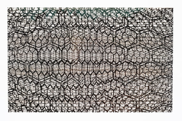
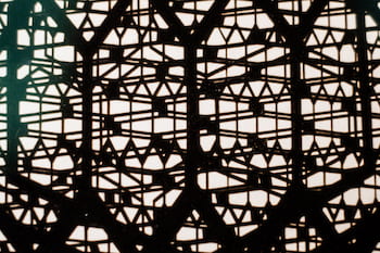
This last form, graphite, is at first glance the most mundane, but thin sheets of it host a wealth of uncommon physics. Research into individual atom-thick sheets of graphite—called graphene—took off after 2004 when scientists developed a reliable way to produce it (using everyday adhesive tape to repeatedly peel layers apart). In 2010 early experiments demonstrating the quantum richness of graphene earned two researchers the Nobel Prize in physics.

In recent years, graphene has kept on giving. Researchers have discovered that stacking layers of graphene two or three at a time (called, respectively, bilayer graphene or trilayer graphene) and twisting the layers relative to each other opens fertile new territory for scientists to explore. Research into these stacked sheets of graphene is like the Wild West, complete with the lure of striking gold and the uncertainty of uncharted territory.

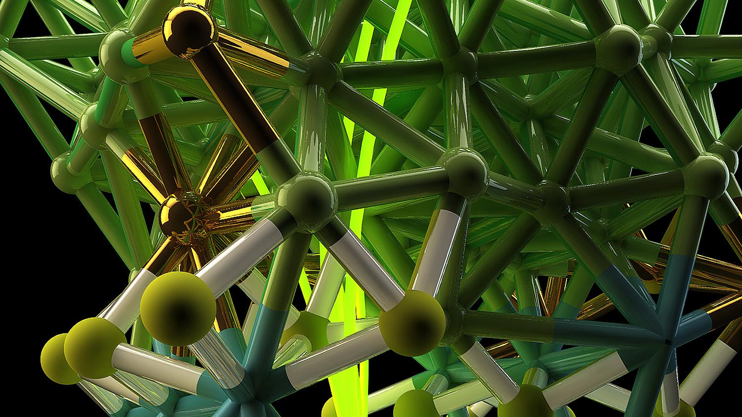
Researchers at JQI and the Condensed Matter Theory Center (CMTC) at the University of Maryland, including JQI Fellows Sankar Das Sarma and Jay Sau and others, are busy creating the theoretical physics foundation that will be a map of this new landscape. And there is a lot to map; the phenomena in graphene range from the familiar like magnetism to more exotic things like strange metallicity, different versions of the quantum Hall effect, and the Pomeranchuk effect—each of which involve electrons coordinating to produce unique behaviors. One of the most promising veins for scientific treasure is the appearance of superconductivity (lossless electrical flow) in stacked graphene.

“Here is a system where almost every interesting quantum phase of matter that theorists ever could imagine shows up in a single system as the twist angle, carrier density, and temperature are tuned in a single sample in a single experiment,” says Das Sarma, who is also the Director of the CMTC. “Sounds like magic or science fantasy, except it is happening every day in at least ten laboratories in the world.”

The richness and diversity of the electrical behaviors in graphene stacks has inspired a stampede of research. The 2021 American Physical Society March Meeting included 13 sessions addressing the topics of graphene or twisted bilayers, and Das Sarma hosted a day long virtual conference in June for researchers to discuss twisted graphene and the related research inspired by the topic. The topic of stacked graphene is extensively represented in scientific journals, and the online arXiv preprint server has over 2,000 articles posted about “bilayer graphene”—nearly 1,000 since 2018.

Perhaps surprisingly, graphene’s wealth of quantum research opportunities is tied to its physical simplicity.

An October 18, 2021 JQI news release by Bailey Bedford, which originated the news item, explains why researchers have described a twist found in graphene as ‘magic’,

Researchers have discovered that at a special, small twist angle (about 1.1 degrees)—whimsically named the “magic angle”—the environment is just right to create strong interactions that radically change its properties. When that precise angle is reached, the electrons tend to cluster around certain areas of the graphene, and new electrical behaviors suddenly appear as if summoned with a dramatic magician’s flourish. Magic angle graphene behaves as a poorly-conducting insulator in some circumstances and in other cases goes to the opposite extreme of being a superconductor—a material that transports electricity without any loss of energy.

The discovery of magic-angle graphene and that it has certain quantum behaviors similar to a high-temperature superconductor was the Physics World 2018 Breakthrough of the Year. Superconductors have many valuable potential uses, like revolutionizing energy infrastructure and making efficient maglev trains. Finding a convenient, room-temperature superconductor has been a holy grail for scientists.

I haven’t done to justice to this piece and, so, for anyone interested in graphene, superconductors, and electronics I recommend reading the piece (October 18, 2021 JQI news release by Bailey Bedford) in its entirety where you’ll also find references to these articles and more,

Reference Publication

Related JQI Articles

Jiggly jell-o as a new hydrogen fuel catalyst

Jello [uploaded from https://www.organicauthority.com/eco-chic-table/new-jell-o-mold-jiggle-chic-holidays]

I’m quite intrigued by this ‘jell-o’ story. It’s hard to believe a childhood dessert might prove to have an application as a catalyst for producing hydrogen fuel. From a December 14, 2018 news item on Nanowerk,

A cheap and effective new catalyst developed by researchers at the University of California, Berkeley, can generate hydrogen fuel from water just as efficiently as platinum, currently the best — but also most expensive — water-splitting catalyst out there.

The catalyst, which is composed of nanometer-thin sheets of metal carbide, is manufactured using a self-assembly process that relies on a surprising ingredient: gelatin, the material that gives Jell-O its jiggle.

Two-dimensional metal carbides spark a reaction that splits water into oxygen and valuable hydrogen gas. Berkeley researchers have discovered an easy new recipe for cooking up these nanometer-thin sheets that is nearly as simple as making Jell-O from a box. (Xining Zang graphic, copyright Wiley)

A December 13, 2018 University of California at Berkeley (UC Berkeley) news release by Kara Manke (also on EurekAlert but published on Dec. 14, 2018), which originated the news item, provides more technical detail,

“Platinum is expensive, so it would be desirable to find other alternative materials to replace it,” said senior author Liwei Lin, professor of mechanical engineering at UC Berkeley. “We are actually using something similar to the Jell-O that you can eat as the foundation, and mixing it with some of the abundant earth elements to create an inexpensive new material for important catalytic reactions.”

The work appears in the Dec. 13 [2018] print edition of the journal Advanced Materials.

A zap of electricity can break apart the strong bonds that tie water molecules together, creating oxygen and hydrogen gas, the latter of which is an extremely valuable source of energy for powering hydrogen fuel cells. Hydrogen gas can also be used to help store energy from renewable yet intermittent energy sources like solar and wind power, which produce excess electricity when the sun shines or when the wind blows, but which go dormant on rainy or calm days.

A black and white image of metal carbide under high magnification.

When magnified, the two-dimensional metal carbides resemble sheets of cell[o]phane. (Xining Zang photo, copyright Wiley)

But simply sticking an electrode in a glass of water is an extremely inefficient method of generating hydrogen gas. For the past 20 years, scientists have been searching for catalysts that can speed up this reaction, making it practical for large-scale use.

“The traditional way of using water gas to generate hydrogen still dominates in industry. However, this method produces carbon dioxide as byproduct,” said first author Xining Zang, who conducted the research as a graduate student in mechanical engineering at UC Berkeley. “Electrocatalytic hydrogen generation is growing in the past decade, following the global demand to lower emissions. Developing a highly efficient and low-cost catalyst for electrohydrolysis will bring profound technical, economical and societal benefit.”

To create the catalyst, the researchers followed a recipe nearly as simple as making Jell-O from a box. They mixed gelatin and a metal ion — either molybdenum, tungsten or cobalt — with water, and then let the mixture dry.

“We believe that as gelatin dries, it self-assembles layer by layer,” Lin said. “The metal ion is carried by the gelatin, so when the gelatin self-assembles, your metal ion is also arranged into these flat layers, and these flat sheets are what give Jell-O its characteristic mirror-like surface.”

Heating the mixture to 600 degrees Celsius triggers the metal ion to react with the carbon atoms in the gelatin, forming large, nanometer-thin sheets of metal carbide. The unreacted gelatin burns away.

The researchers tested the efficiency of the catalysts by placing them in water and running an electric current through them. When stacked up against each other, molybdenum carbide split water the most efficiently, followed by tungsten carbide and then cobalt carbide, which didn’t form thin layers as well as the other two. Mixing molybdenum ions with a small amount of cobalt boosted the performance even more.

“It is possible that other forms of carbide may provide even better performance,” Lin said.

On the left, an illustration of blue spheres, representing gelatin molecules, arranged in a lattice shape. On the right, an illustration of thin sheets of metal carbide.

Molecules in gelatin naturally self-assemble in flat sheets, carrying the metal ions with them (left). Heating the mixture to 600 degrees Celsius burns off the gelatin, leaving nanometer-thin sheets of metal carbide. (Xining Zang illustration, copyright Wiley)

The two-dimensional shape of the catalyst is one of the reasons why it is so successful. That is because the water has to be in contact with the surface of the catalyst in order to do its job, and the large surface area of the sheets mean that the metal carbides are extremely efficient for their weight.

Because the recipe is so simple, it could easily be scaled up to produce large quantities of the catalyst, the researchers say.

“We found that the performance is very close to the best catalyst made of platinum and carbon, which is the gold standard in this area,” Lin said. “This means that we can replace the very expensive platinum with our material, which is made in a very scalable manufacturing process.”

Co-authors on the study are Lujie Yang, Buxuan Li and Minsong Wei of UC Berkeley, J. Nathan Hohman and Chenhui Zhu of Lawrence Berkeley National Lab; Wenshu Chen and Jiajun Gu of Shanghai Jiao Tong University; Xiaolong Zou and Jiaming Liang of the Shenzhen Institute; and Mohan Sanghasadasa of the U.S. Army RDECOM AMRDEC.

Here’s a link to and a citation for the paper,

Self‐Assembly of Large‐Area 2D Polycrystalline Transition Metal Carbides for Hydrogen Electrocatalysis by Xining Zang, Wenshu Chen, Xiaolong Zou, J. Nathan Hohman, Lujie Yang
Buxuan Li, Minsong Wei, Chenhui Zhu, Jiaming Liang, Mohan Sanghadasa, Jiajun Gu, Liwei Lin. Advanced Materials Volume30, Issue 50 December 13, 2018 1805188 DOI: https://doi.org/10.1002/adma.201805188 First published [online]: 09 October 2018

This paper is behind a paywall.

Bendable phones that are partially organic

It’s been about nine  or 10 years since I first heard about bendable phones (my September 29, 2010 posting). The concept keeps popping up from time to time (my April 25, 2017 posting) and this time, we have Australian scientists to thank for this latest work described in an October 5, 2018 news item on Nanowerk (Note: A link has been removed),

Engineers at ANU [Australian National University] have invented a semiconductor with organic and inorganic materials that can convert electricity into light very efficiently, and it is thin and flexible enough to help make devices such as mobile phones bendable (Advanced Materials, “Efficient and Layer-Dependent Exciton Pumping across Atomically Thin Organic–Inorganic Type-I Heterostructures”).

The invention also opens the door to a new generation of high-performance electronic devices made with organic materials that will be biodegradable or that can be easily recycled, promising to help substantially reduce e-waste.

An October 5, 2018 ANU press release (also on EurekAlert but published October 4, 2018) expands on the theme,

The huge volumes of e-waste generated by discarded electronic devices around the world is causing irreversible damage to the environment. Australia produces 200,000 tonnes of e-waste every year – only four per cent of this waste is recycled.

The organic component has the thickness of just one atom – made from just carbon and hydrogen – and forms part of the semiconductor that the ANU team developed. The inorganic component has the thickness of around two atoms. The hybrid structure can convert electricity into light efficiently for displays on mobile phones, televisions and other electronic devices.

Lead senior researcher Associate Professor Larry Lu said the invention was a major breakthrough in the field.

“For the first time, we have developed an ultra-thin electronics component with excellent semiconducting properties that is an organic-inorganic hybrid structure and thin and flexible enough for future technologies, such as bendable mobile phones and display screens,” said Associate Professor Lu from the ANU Research School of Engineering.

PhD researcher Ankur Sharma, who recently won the ANU 3-Minute Thesis competition, said experiments demonstrated the performance of their semiconductor would be much more efficient than conventional semiconductors made with inorganic materials such as silicon.

“We have the potential with this semiconductor to make mobile phones as powerful as today’s supercomputers,” said Mr Sharma from the ANU Research School of Engineering.

“The light emission from our semiconducting structure is very sharp, so it can be used for high-resolution displays and, since the materials are ultra-thin, they have the flexibility to be made into bendable screens and mobile phones in the near future.”

The team grew the organic semiconductor component molecule by molecule, in a similar way to 3D printing. The process is called chemical vapour deposition.

“We characterised the opto-electronic and electrical properties of our invention to confirm the tremendous potential of it to be used as a future semiconductor component,” Associate Professor Lu said.

“We are working on growing our semiconductor component on a large scale, so it can be commercialised in collaboration with prospective industry partners.”

Here’s a link to and a citation for the paper,

Efficient and Layer‐Dependent Exciton Pumping across Atomically Thin Organic–Inorganic Type‐I Heterostructures by Linglong Zhang, Ankur Sharma, Yi Zhu, Yuhan Zhang, Bowen Wang, Miheng Dong, Hieu T. Nguyen, Zhu Wang, Bo Wen, Yujie Cao, Boqing Liu, Xueqian Sun, Jiong Yang, Ziyuan Li. Advanced Materials Volume30, Issue 40 1803986 (October 4, 2018) DOI:https://doi.org/10.1002/adma.201803986 First published [onliine]: 30 August 2018

This paper is behind a paywall.

Where do I stand? a graphene artwork

A May 2,2019 news item on Nanowerk describes some graphene-based artwork being created at Rice University (Texas, US), Note: A link has been removed,

When you read about electrifying art, “electrifying” isn’t usually a verb. But an artist working with a Rice University lab is in fact making artwork that can deliver a jolt.

The Rice lab of chemist James Tour introduced laser-induced graphene (LIG) to the world in 2014, and now the researchers are making art with the technique, which involves converting carbon in a common polymer or other material into microscopic flakes of graphene.

The “ink” in “Where Do I Stand?” by artist Joseph Cohen is actually laser-induced graphene (LIG). The design shows Cohen’s impression of what LIG looks like at the microscopic level. The work was produced in the Rice University lab where the technique of creating LIG was invented. Photo by Jeff Fitlow
A detail from “Where Do I Stand?” by artist Joseph Cohen, who created the work at Rice University using laser-induced graphene as the medium. Photo by Jeff Fitlow

A May 2, 2019 Rice university news release (also received via email), which originated the news item, describes laser-induced graphene (LIG) and the art in more detail (Note: Links have been removed),

LIG is metallic and conducts electricity. The interconnected flakes are effectively a wire that could empower electronic artworks.

The paper in the American Chemical Society journal ACS Applied Nano Materials – simply titled “Graphene Art” – lays out how the lab and Houston artist and co-author Joseph Cohen generated LIG portraits and prints, including a graphene-inspired landscape called “Where Do I Stand?”

While the work isn’t electrified, Cohen said it lays the groundwork for future possibilities.

“That’s what I would like to do,” he said. “Not make it kitsch or play off the novelty, but to have it have some true functionality that allows greater awareness about the material and opens up the experience.”

Cohen created the design in an illustration program and sent it directly to the industrial engraving laser Tour’s lab uses to create LIG on a variety of materials. The laser burned the artist’s fine lines into the substrate, in this case archive-quality paper treated with fire retardant.

The piece, which was part of Cohen’s exhibit at Rice’s BioScience Research Collaborative last year, peers into the depths of what a viewer shrunken to nanoscale might see when facing a field of LIG, with overlapping hexagons – the basic lattice of atom-thick graphene – disappearing into the distance.

“You’re looking at this image of a 3D foam matrix of laser-induced graphene and it’s actually made of LIG,” he said. “I didn’t base it on anything; I was just thinking about what it would look like. When I shared it with Jim, he said, ‘Wow, that’s what it would look like if you could really blow this up.’”

Cohen said his art is about media specificity.

“In terms of the artistic application, you’re not looking at a representation of something, as traditionally we would in the history of art,” he said. “Each piece is 100% original. That’s the key.”

He developed an interest in nanomaterials as media for his art when he began work with Rice alumnus Daniel Heller, a bioengineer at Memorial Sloan Kettering Cancer Center in New York who established an artist-in-residency position in his lab.

After two years of creating with carbon nanotube-infused paint, Cohen attended an Electrochemical Society conference and met Tour, who in turn introduced him to Rice chemists Bruce Weisman and Paul Cherukuri, who further inspired his investigation of nanotechnology.

The rest is art history.

It would be incorrect to think of the process as “printing,” Tour said. Instead of adding a substance to the treated paper, substance is burned away as the laser turns the surface into foamlike flakes of interconnected graphene.

The art itself can be much more than eye candy, given LIG’s potential for electronic applications like sensors or as triboelectric generators that turn mechanical actions into current.

“You could put LIG on your back and have it flash LEDs with every step you take,” Tour said.

The fact that graphene is a conductor — unlike paint, ink or graphite from a pencil — makes it particularly appealing to Cohen, who expects to take advantage of that capability in future works.

“It’s art with a capital A that is trying to do the most that it can with advancements in science and technology,” he said. “If we look back historically, from the Renaissance to today, the highest forms of art push the limits of human understanding.”

Here’s a link to and a citation for the paper,

Graphene Art by Yieu Chyan, Joseph Cohen, Winston Wang, Chenhao Zhang, and James M. Tour. ACS Appl. Nano Mater., Article ASAP DOI: 10.1021/acsanm.9b00391 Publication Date (Web): April 23, 2019

Copyright © 2019 American Chemical Society

This paper appears to be open access.

Because I can’t resist the delight beaming from these faces,

maging with laser-induced graphene (LIG) was taken to a new level in a Rice University lab. From left, chemist James Tour, holding a portrait of himself in LIG; artist Joseph Cohen, holding his work “Where Do I Stand?”; and Yieu Chyan, a Rice graduate student and lead author of a new paper detailing the process used to create the art. Photo by Jeff Fitlow

Golden nanoglue

This starts out as a graphene story before taking an abrupt turn. From a June 5, 2018 news item on Nanowerk,

Graphene has undoubtedly been the most popular research subject of nanotechnology during recent years. Made of pure carbon, this material is in principle easy to manufacture: take ordinary graphite and peel one layer off with Scotch tape. The material thus obtained is two-dimensional, yielding unique properties, different from those in three-dimensional materials.

Graphene, however, lacks one important property, semiconductivity, which complicates its usage in electronics applications. Scientists have therefore started the quest of other two-dimensional materials with this desired property.

Molybdenum disulfide, MoS2 is among the most promising candidates. Like graphene, MoS2 consists of layers, interacting weakly with one another. In addition to being a semiconductor, the semiconducting properties of MoS2 change depending on the number of atomic layers.

A June 5, 2018 University of Oulu press release, which originated the news item,  gives more detail about the work,

For the one or few layer MoS2 to be useful in applications, one must be able to join it to other components. What is thus needed is such a metallic conductor that electric current can easily flow between the conductor and the semiconductor. In the case of MoS2, a promising conductor is provided by nickel, which also has other desired properties from the applications point of view.

However, an international collaboration, led by the Nano and molecular systems research unit at the University of Oulu has recently discovered that nanoparticles made of nickel do not attach to MoS2. One needs gold, which ‘glues’ the conductor and the component together. Says docent Wei Cao of NANOMO: “The synthesis is performed through a sonochemical method.” Sonochemistry is a method where chemical reactions are established using ultrasound. NANOMO scientist Xinying Shi adds: “The semiconductor and metal can be bridged either by the crystallized gold nanoparticles, or by the newly formed MoS2-Au-Ni ternary alloy.”

The nanojunction so established has a very small electrical resistivity. It also preserves the semiconducting and magnetic properties of MoS2. In addition, the new material has desirable properties beyond those of the original constituents. For example, it acts as a photocatalyst, which works much more efficiently than pure MoS2. Manufacturing the golden nanojunction is easy and cheap, which makes the new material attractive from the applications point of view.

Here’s a link to and a citation for the paper,

Metallic Contact between MoS2 and Ni via Au Nanoglue by Xinying Shi, Sergei Posysaev, Marko Huttula, Vladimir Pankratov, Joanna Hoszowska, Jean‐Claude Dousse, Faisal Zeeshan, Yuran Niu, Alexei Zakharov, Taohai Li. Small Volume 14, Issue22 May 29, 2018 1704526 First published online: 24 April 2018 https://doi.org/10.1002/smll.201704526

This paper is behind a paywall.

There is a pretty illustration of the ‘golden nanojunctions’,

Golden nanoglue (Courtesy of the University of Oulu)

Using sound to transfer quantum information

It seems sound is becoming more prominent as a means of science data communication (data sonification) and in this upcoming case, data transfer. From a June 5, 2018 news item on ScienceDaily,

Quantum physics is on the brink of a technological breakthrough: new types of sensors, secure data transmission methods and maybe even computers could be made possible thanks to quantum technologies. However, the main obstacle here is finding the right way to couple and precisely control a sufficient number of quantum systems (for example, individual atoms).

A team of researchers from TU Wien and Harvard University has found a new way to transfer the necessary quantum information. They propose using tiny mechanical vibrations. The atoms are coupled with each other by ‘phonons’ — the smallest quantum mechanical units of vibrations or sound waves.

A June 5, 2018 Technical University of Vienna (TU Wien) press release, which originated the news item, explains the work in greater detail,

“We are testing tiny diamonds with built-in silicon atoms – these quantum systems are particularly promising,” says Professor Peter Rabl from TU Wien. “Normally, diamonds are made exclusively of carbon, but adding silicon atoms in certain places creates defects in the crystal lattice where quantum information can be stored.” These microscopic flaws in the crystal lattice can be used like a tiny switch that can be switched between a state of higher energy and a state of lower energy using microwaves.

Together with a team from Harvard University, Peter Rabl’s research group has developed a new idea to achieve the targeted coupling of these quantum memories within the diamond. One by one they can be built into a tiny diamond rod measuring only a few micrometres in length, like individual pearls on a necklace. Just like a tuning fork, this rod can then be made to vibrate – however, these vibrations are so small that they can only be described using quantum theory. It is through these vibrations that the silicon atoms can form a quantum-mechanical link to each other.

“Light is made from photons, the quantum of light. In the same way, mechanical vibrations or sound waves can also be described in a quantum-mechanical manner. They are comprised of phonons – the smallest possible units of mechanical vibration,” explains Peter Rabl. As the research team has now been able to show using simulation calculations, any number of these quantum memories can be linked together in the diamond rod thanks to these phonons. The individual silicon atoms are “switched on and off” using microwaves. During this process, they emit or absorb phonons. This creates a quantum entanglement of different silicon defects, thus allowing quantum information to be transferred.

The road to a scalable quantum network
Until now it was not clear whether something like this was even possible: “Usually you would expect the phonons to be absorbed somewhere, or to come into contact with the environment and thus lose their quantum mechanical properties,” says Peter Rabl. “Phonons are the enemy of quantum information, so to speak. But with our calculations, we were able to show that, when controlled appropriately using microwaves, the phonons are in fact useable for technical applications.”

The main advantage of this new technology lies in its scalability: “There are many ideas for quantum systems that, in principle, can be used for technological applications. The biggest problem is that it is very difficult to connect enough of them to be able to carry out complicated computing operations,” says Peter Rabl. The new strategy of using phonons for this purpose could pave the way to a scalable quantum technology.

Here’s a link to and a citation for the paper,

Phonon Networks with Silicon-Vacancy Centers in Diamond Waveguides by M.-A. Lemonde, S. Meesala, A. Sipahigil, M. J. A. Schuetz, M. D. Lukin, M. Loncar, and P. Rabl. Phys. Rev. Lett. 120 (21), 213603 DOI:https://doi.org/10.1103/PhysRevLett.120.213603 Published 25 May 2018

This paper is behind a paywall.

Creating cheap, small carbon nanotubes

The excitement fairly crackles off the video,

A May 24, 2018 news item on Nanowerk announces the research,

Imagine a box you plug into the wall that cleans your toxic air and pays you cash.

That’s essentially what Vanderbilt University researchers produced after discovering the blueprint for turning the carbon dioxide into carbon nanotubes with small diameters.

Carbon nanotubes are supermaterials that can be stronger than steel and more conductive than copper. The reason they’re not in every application from batteries to tires is that these amazing properties only show up in the tiniest nanotubes, which are extremely expensive. Not only did the Vanderbilt team show they can make these materials from carbon dioxide sucked from the air, but how to do this in a way that is much cheaper than any other method out there.

I’m not sure what ‘small’ means in this context. I’ve heard of long and short carbon nanotubes (CNTs) and also of single-walled, multi-walled, and double-walled CNTs. I wish there’d been an an explanation and measurements for ‘small diameter CNTs’. That nitpick aside, a May 23, 2018 Vanderbilt University news release by Heidi Hall adds a few more technical details,

These materials, which Assistant Professor of Mechanical Engineering Cary Pint calls “black gold,” could steer the conversation from the negative impact of emissions to how we can use them in future technology.

“One of the most exciting things about what we’ve done is use electrochemistry to pull apart carbon dioxide into elemental constituents of carbon and oxygen and stitch together, with nanometer precision, those carbon atoms into new forms of matter,” Pint said. “That opens the door to being able to generate really valuable products with carbon nanotubes.

“These could revolutionize the world.”

In a report published today in ACS [American Chemical Society] Applied Materials and Interfaces, Pint, interdisciplinary material science Ph.D. student Anna Douglas and their team describe how tiny nanoparticles 10,000 times smaller than a human hair can be produced from coatings on stainless steel surfaces. The key was making them small enough to be valuable.

“The cheapest carbon nanotubes on the market cost around $100-200 per kilogram,” Douglas said. “Our research advance demonstrates a pathway to synthesize carbon nanotubes better in quality than these materials with lower cost and using carbon dioxide captured from the air.”

But making small nanotubes is no small task. The research team showed that a process called Ostwald ripening — where the nanoparticles that grow the carbon nanotubes change in size to larger diameters — is a key contender against producing the infinitely more useful size. The team showed they could partially overcome this by tuning electrochemical parameters to minimize these pesky large nanoparticles.

side-by-side photos showing stainless steel plate becoming covered in carbon nanotubes (which look like lumps of ash or mud)
Small diameter carbon nanotubes grown on a stainless steel surface. (Pint Lab/Vanderbilt University)

This core technology led Pint and Douglas to co-found SkyNano LLC, a company focused on building upon the science of this process to scale up and commercialize products from these materials.

“What we’ve learned is the science that opens the door to now build some of the most valuable materials in our world, such as diamonds and single-walled carbon nanotubes, from carbon dioxide that we capture from air through our process,” Pint said.

Here’s a link to and a citation for the paper,

Toward Small-Diameter Carbon Nanotubes Synthesized from Captured Carbon Dioxide: Critical Role of Catalyst Coarsening by Anna Douglas, Rachel Carter, Mengya Li, and Cary L. Pint. ACS Appl. Mater. Interfaces, Article ASAP DOI: 10.1021/acsami.8b02834 Publication Date (Web): May 1, 2018

Copyright © 2018 American Chemical Society

This paper is behind a paywall.

Regarding the start-up, SkyNano, which Douglas and Pint have co-founded, it looks to be at a  very early stage.

See Nobel prize winner’s (Kostya Novoselov) collaborative art/science video project on August 17, 2018 (Manchester, UK)

Dr. Konstantin (Kostya) Novoselov, one of the two scientists at the University of Manchester (UK) who were awarded Nobel prizes for their work with graphene, has embarked on an artistic career of sorts. From an August 8, 2018 news item on Nanowwerk,

Nobel prize-winning physicist Sir Kostya Novoselov worked with artist Mary Griffiths to create Prospect Planes – a video artwork resulting from months of scientific and artistic research and experimentation using graphene.

Prospect Planes will be unveiled as part of The Hexagon Experiment series of events at the Great Exhibition of the North 2018, Newcastle, on August 17 [2018].

An August 9, 2018 University of Manchester press release, which originated the news item (differences in the dates are likely due to timezones), describes the art/science project in some detail,

The fascinating video art project aims to shed light on graphene’s unique qualities and potential.

Providing a fascinating insight into scientific research into graphene, Prospect Planes began with a graphite drawing by Griffiths, symbolising the chemical element carbon.

This was replicated in graphene by Sir Kostya Novoselov, creating a microscopic 2D graphene version of Griffiths’ drawing just one atom thick and invisible to the naked eye.

They then used Raman spectroscopy to record a molecular fingerprint of the graphene image, using that fingerprint to map a digital visual representation of graphene’s unique qualities.

The six-part Hexagon Experiment series was inspired by the creativity of the Friday evening sessions that led to the isolation of graphene at The University of Manchester by Novoselov and Sir Andre Geim.

Mary Griffiths, has previously worked on other graphene artworks including From Seathwaite an installation in the National Graphene Institute, which depicts the story of graphite and graphene – its geography, geology and development in the North West of England.

Mary Griffiths, who is also Senior Curator at The Whitworth said: “Having previously worked alongside Kostya on other projects, I was aware of his passion for art. This has been a tremendously exciting and rewarding project, which will help people to better understand the unique qualities of graphene, while bringing Manchester’s passion for collaboration and creativity across the arts, industry and science to life.

“In many ways, the story of the scientific research which led to the creation of Prospect Planes is as exciting as the artwork itself. By taking my pencil drawing and patterning it in 2D with a single layer of graphene atoms, then creating an animated digital work of art from the graphene data, we hope to provoke further conversations about the nature of the first 2D material and the potential benefits and purposes of graphene.”

Sir Kostya Novoselov said: “In this particular collaboration with Mary, we merged two existing concepts to develop a new platform, which can result in multiple art projects. I really hope that we will continue working together to develop this platform even further.”

The Hexagon Experiment is taking place just a few months before the official launch of the £60m Graphene Engineering Innovation Centre, part of a major investment in 2D materials infrastructure across Manchester, cementing its reputation as Graphene City.

Prospect Planes was commissioned by Manchester-based creative music charity Brighter Sound.

The Hexagon Experiment is part of Both Sides Now – a three-year initiative to support, inspire and showcase women in music across the North of England, supported through Arts Council England’s Ambition for Excellence fund.

It took some searching but I’ve found the specific Hexagon event featuring Sir Novoselov’s and Mary Griffin’s work. From ‘The Hexagon Experiment #3: Adventures in Flatland’ webpage,

Lauren Laverne is joined by composer Sara Lowes and visual artist Mary Griffiths to discuss their experiments with music, art and science. Followed by a performance of Sara Lowes’ graphene-inspired composition Graphene Suite, and the unveiling of new graphene art by Mary Griffiths and Professor Kostya Novoselov. Alongside Andre Geim, Novoselov was awarded the Nobel Prize in Physics in 2010 for his groundbreaking experiments with graphene.


About The Hexagon Experiment

Music, art and science collide in an explosive celebration of women’s creativity

A six-part series of ‘Friday night experiments’ featuring live music, conversations and original commissions from pioneering women at the forefront of music, art and science.

Inspired by the creativity that led to the discovery of the Nobel-Prize winning ‘wonder material’ graphene, The Hexagon Experiment brings together the North’s most exciting musicians and scientists for six free events – from music made by robots to a spectacular tribute to an unsung heroine.

Presented by Brighter Sound and the National Graphene Institute at The University of Manchester, as part of the Great Exhibition of the North.

Buy tickets here.

One final comment, the title for the evening appears to have been inspired by a novella, from the Flatland Wikipedia entry (Note: Links have been removed),

Flatland: A Romance of Many Dimensions is a satirical novella by the English schoolmaster Edwin Abbott Abbott, first published in 1884 by Seeley & Co. of London.

Written pseudonymously by “A Square”,[1] the book used the fictional two-dimensional world of Flatland to comment on the hierarchy of Victorian culture, but the novella’s more enduring contribution is its examination of dimensions.[2]

That’s all folks.

ETA August 14, 2018: Not quite all. Hopefully this attempt to add a few details for people not familiar with graphene won’t lead increased confusion. The Hexagon event ‘Advetures in Flatland’ which includes Novoselov’s and Griffiths’ video project features some wordplay based on graphene’s two dimensional nature.

Psst: secret marriage … Buckyballs and Graphene get together!

A March 1, 2018 news item on Nanowerk announces  a new coupling,

Scientists combined buckyballs, [also known as buckminsterfullerenes, fullerenes, or C60] which resemble tiny soccer balls made from 60 carbon atoms, with graphene, a single layer of carbon, on an underlying surface. Positive and negative charges can transfer between the balls and graphene depending on the nature of the surface as well as the structural order and local orientation of the carbon ball. Scientists can use this architecture to develop tunable junctions for lightweight electronic devices.

The researchers have made this illustration of their work available,

Researchers are developing new, lightweight electronics that rapidly conduct electricity by covering a sheet of carbon (graphene) with buckyballs. Electricity is the flow of electrons. On these lightweight structures, electrons as well as positive holes (missing electrons) transfer between the balls and graphene. The team showed that the crystallinity and orientation of the balls, as well as the underlying layer, affected this charge transfer. The top image shows a calculation of the charge density for a specific orientation of the balls on graphene. The blue represents positive charges, while the red is negative. The bottom image shows that the balls are in a close-packed structure. The bright dots correspond to the projected images of columns of buckyball molecules. Courtesy: US Department of Energy Office of Science

A February 28, 2018 US Department of Energy (DoE) Office of Science news release, which originated the news item, provides more detail,

The Impact

Fast-moving electrons and their counterpart, holes, were preserved in graphene with crystalline buckyball overlayers. Significantly, the carbon ball provides charge transfer to the graphene. Scientists expect the transfer to be highly tunable with external voltages. This marriage has ramifications for smart electronics that run longer and do not break as easily, bringing us closer to sensor-embedded smart clothing and robotic skin.

Summary

Charge transfer at the interface between dissimilar materials is at the heart of almost all electronic technologies such as transistors and photovoltaic devices. In this study, scientists studied charge transfer at the interface region of buckyball molecules deposited on graphene, with and without a supporting substrate, such as hexagonal boron nitride. They employed ab initio density functional theory with van der Waals interactions to model the structure theoretically. Van der Waals interactions are weak connections between neutral molecules. The team used high-resolution transmission electron microscopy and electronic transport measurements to characterize experimentally the properties of the interface. The researchers observed that charge transfer between buckyballs and the graphene was sensitive to the nature of the underlying substrate, in addition, to the crystallinity and local orientation of the buckyballs. These studies open an avenue to devices where buckyball layers on top of graphene can serve as electron acceptors and other buckyball layers as electron donors. Even at room temperature, buckyball molecules were orientationally locked into position. This is in sharp contrast to buckyball molecules in un-doped bulk crystalline configurations, where locking occurs only at low temperature. High electron and hole mobilities are preserved in graphene with crystalline buckyball overlayers. This finding has ramifications for the development of organic high-mobility field-effect devices and other high mobility applications.

Here’s a link to and a citation for the paper,

Molecular Arrangement and Charge Transfer in C60 /Graphene Heterostructures by Claudia Ojeda-Aristizabal, Elton J. G. Santos, Seita Onishi, Aiming Yan, Haider I. Rasool, Salman Kahn, Yinchuan Lv, Drew W. Latzke, Jairo Velasco Jr., Michael F. Crommie, Matthew Sorensen, Kenneth Gotlieb, Chiu-Yun Lin, Kenji Watanabe, Takashi Taniguchi, Alessandra Lanzara, and Alex Zettl. ACS Nano, 2017, 11 (5), pp 4686–4693 DOI: 10.1021/acsnano.7b00551 Publication Date (Web): April 24, 2017

Copyright © 2017 American Chemical Society

This paper is behind a paywall.

Do you want that coffee with some graphene on toast?

These scientists are excited:

For those who prefer text, here’s the Rice University Feb. 13, 2018 news release (received via email and available online here and on EurekAlert here) Note: Links have been removed),

Rice University scientists who introduced laser-induced graphene (LIG) have enhanced their technique to produce what may become a new class of edible electronics.

The Rice lab of chemist James Tour, which once turned Girl Scout cookies into graphene, is investigating ways to write graphene patterns onto food and other materials to quickly embed conductive identification tags and sensors into the products themselves.

“This is not ink,” Tour said. “This is taking the material itself and converting it into graphene.”

The process is an extension of the Tour lab’s contention that anything with the proper carbon content can be turned into graphene. In recent years, the lab has developed and expanded upon its method to make graphene foam by using a commercial laser to transform the top layer of an inexpensive polymer film.

The foam consists of microscopic, cross-linked flakes of graphene, the two-dimensional form of carbon. LIG can be written into target materials in patterns and used as a supercapacitor, an electrocatalyst for fuel cells, radio-frequency identification (RFID) antennas and biological sensors, among other potential applications.

The new work reported in the American Chemical Society journal ACS Nano demonstrated that laser-induced graphene can be burned into paper, cardboard, cloth, coal and certain foods, even toast.

“Very often, we don’t see the advantage of something until we make it available,” Tour said. “Perhaps all food will have a tiny RFID tag that gives you information about where it’s been, how long it’s been stored, its country and city of origin and the path it took to get to your table.”

He said LIG tags could also be sensors that detect E. coli or other microorganisms on food. “They could light up and give you a signal that you don’t want to eat this,” Tour said. “All that could be placed not on a separate tag on the food, but on the food itself.”

Multiple laser passes with a defocused beam allowed the researchers to write LIG patterns into cloth, paper, potatoes, coconut shells and cork, as well as toast. (The bread is toasted first to “carbonize” the surface.) The process happens in air at ambient temperatures.

“In some cases, multiple lasing creates a two-step reaction,” Tour said. “First, the laser photothermally converts the target surface into amorphous carbon. Then on subsequent passes of the laser, the selective absorption of infrared light turns the amorphous carbon into LIG. We discovered that the wavelength clearly matters.”

The researchers turned to multiple lasing and defocusing when they discovered that simply turning up the laser’s power didn’t make better graphene on a coconut or other organic materials. But adjusting the process allowed them to make a micro supercapacitor in the shape of a Rice “R” on their twice-lased coconut skin.

Defocusing the laser sped the process for many materials as the wider beam allowed each spot on a target to be lased many times in a single raster scan. That also allowed for fine control over the product, Tour said. Defocusing allowed them to turn previously unsuitable polyetherimide into LIG.

“We also found we could take bread or paper or cloth and add fire retardant to them to promote the formation of amorphous carbon,” said Rice graduate student Yieu Chyan, co-lead author of the paper. “Now we’re able to take all these materials and convert them directly in air without requiring a controlled atmosphere box or more complicated methods.”

The common element of all the targeted materials appears to be lignin, Tour said. An earlier study relied on lignin, a complex organic polymer that forms rigid cell walls, as a carbon precursor to burn LIG in oven-dried wood. Cork, coconut shells and potato skins have even higher lignin content, which made it easier to convert them to graphene.

Tour said flexible, wearable electronics may be an early market for the technique. “This has applications to put conductive traces on clothing, whether you want to heat the clothing or add a sensor or conductive pattern,” he said.

Rice alumnus Ruquan Ye is co-lead author of the study. Co-authors are Rice graduate student Yilun Li and postdoctoral fellow Swatantra Pratap Singh and Professor Christopher Arnusch of Ben-Gurion University of the Negev, Israel. Tour is the T.T. and W.F. Chao Chair in Chemistry as well as a professor of computer science and of materials science and nanoengineering at Rice.

The Air Force Office of Scientific Research supported the research.

Here’s a link to and a citation for the paper,

Laser-Induced Graphene by Multiple Lasing: Toward Electronics on Cloth, Paper, and Food by Yieu Chyan, Ruquan Ye†, Yilun Li, Swatantra Pratap Singh, Christopher J. Arnusch, and James M. Tour. ACS Nano DOI: 10.1021/acsnano.7b08539 Publication Date (Web): February 13, 2018

Copyright © 2018 American Chemical Society

This paper is behind a paywall.

h/t Feb. 13, 2018 news item on Nanowerk