An adhesive that US and Chinese scientists have developed shows great promise not just for bandages but wearable robotics too. From a December 14, 2018 news item on Nanowerk,
Researchers from the Harvard John A. Paulson School of Engineering and Applied Sciences (SEAS) and Xi’an Jiaotong University in China have developed a new type of adhesive that can strongly adhere wet materials — such as hydrogel and living tissue — and be easily detached with a specific frequency of light.
The adhesives could be used to attach and painlessly detach wound dressings, transdermal drug delivery devices, and wearable robotics.
“Strong adhesion usually requires covalent bonds, physical interactions, or a combination of both,” said Yang Gao, first author of the paper and researcher at Xi’an Jiaotong University. “Adhesion through covalent bonds is hard to remove and adhesion through physical interactions usually requires solvents, which can be time-consuming and environmentally harmful. Our method of using light to trigger detachment is non-invasive and painless.”
The adhesive uses an aqueous solution of polymer chains spread between two, non-sticky materials — like jam between two slices of bread. On their own, the two materials adhere poorly together but the polymer chains act as a molecular suture, stitching the two materials together by forming a network with the two preexisting polymer networks. This process is known as topological entanglement.
When exposed to ultra-violet light, the network of stitches dissolves, separating the two materials.
The researchers, led by Zhigang Suo, the Allen E. and Marilyn M. Puckett Professor of Mechanics and Materials at SEAS, tested adhesion and detachment on a range of materials, sticking together hydrogels; hydrogels and organic tissue; elastomers; hydrogels and elastomers; and hydrogels and inorganic solids.
“Our strategy works across a range of materials and may enable broad applications,” said Kangling Wu, co-lead author and researcher at Xi’an Jiaotong University in China. While the researchers focused on using UV light to trigger detachment, their work suggests the possibility that the stitching polymer could detach with near-infrared light, a feature which could be applied to a range of new medical procedures.
“In nature, wet materials don’t like to adhere together,” said Suo. “We have discovered a general approach to overcome this challenge. Our molecular sutures can strongly adhere wet materials together. Furthermore, the strong adhesion can be made permanent, transient, or detachable on demand, in response to a cue. So, as we see it, nature is full of loopholes, waiting to be stitched.”
Here’s a link to and a citation for the paper,
Photodetachable Adhesion by Yang Gao, Kangling Wu, Zhigang Suo. https://doi.org/10.1002/adma.201806948 First published: 14 December 2018
Light-harvesting devices—I like that better than solar cells or the like but I think that the term serves as a category rather than a name/label for a specific device. Enough musing. A December 17, 2018 news item on Nanowerk describes the latest about graphene and light-harvesting devices (Note: A link has been removed,
An international research team, co-led by a physicist at the University of California, Riverside, has discovered a new mechanism for ultra-efficient charge and energy flow in graphene, opening up opportunities for developing new types of light-harvesting devices.
The researchers fabricated pristine graphene — graphene with no impurities — into different geometric shapes, connecting narrow ribbons and crosses to wide open rectangular regions. They found that when light illuminated constricted areas, such as the region where a narrow ribbon connected two wide regions, they detected a large light-induced current, or photocurrent.
The finding that pristine graphene can very efficiently convert light into electricity could lead to the development of efficient and ultrafast photodetectors — and potentially more efficient solar panels.
Graphene, a 1-atom thick sheet of carbon atoms arranged in a hexagonal lattice, has many desirable material properties, such as high current-carrying capacity and thermal conductivity. In principle, graphene can absorb light at any frequency, making it ideal material for infrared and other types of photodetection, with wide applications in bio-sensing, imaging, and night vision.
In most solar energy harvesting devices, a photocurrent arises only in the presence of a junction between two dissimilar materials, such as “p-n” junctions, the boundary between two types of semiconductor materials. The electrical current is generated in the junction region and moves through the distinct regions of the two materials.
“But in graphene, everything changes,” said Nathaniel Gabor, an associate professor of physics at UCR, who co-led the research project. “We found that photocurrents may arise in pristine graphene under a special condition in which the entire sheet of graphene is completely free of excess electronic charge. Generating the photocurrent requires no special junctions and can instead be controlled, surprisingly, by simply cutting and shaping the graphene sheet into unusual configurations, from ladder-like linear arrays of contacts, to narrowly constricted rectangles, to tapered and terraced edges.”
Pristine graphene is completely charge neutral, meaning there is no excess electronic charge in the material. When wired into a device, however, an electronic charge can be introduced by applying a voltage to a nearby metal. This voltage can induce positive charge, negative charge, or perfectly balance negative and positive charges so the graphene sheet is perfectly charge neutral.
“The light-harvesting device we fabricated is only as thick as a single atom,” Gabor said. “We could use it to engineer devices that are semi-transparent. These could be embedded in unusual environments, such as windows, or they could be combined with other more conventional light-harvesting devices to harvest excess energy that is usually not absorbed. Depending on how the edges are cut to shape, the device can give extraordinarily different signals.”
The research team reports this first observation of an entirely new physical mechanism — a photocurrent generated in charge-neutral graphene with no need for p-n junctions — in Nature Nanotechnology today [Dec. 17, 2018].
Previous work by the Gabor lab showed a photocurrent in graphene results from highly excited “hot” charge carriers. When light hits graphene, high-energy electrons relax to form a population of many relatively cooler electrons, Gabor explained, which are subsequently collected as current. Even though graphene is not a semiconductor, this light-induced hot electron population can be used to generate very large currents.
“All of this behavior is due to graphene’s unique electronic structure,” he said. “In this ‘wonder material,’ light energy is efficiently converted into electronic energy, which can subsequently be transported within the material over remarkably long distances.”
He explained that, about a decade ago, pristine graphene was predicted to exhibit very unusual electronic behavior: electrons should behave like a liquid, allowing energy to be transferred through the electronic medium rather than by moving charges around physically. “But despite this prediction, no photocurrent measurements had been done on pristine graphene devices — until now,” he said.
The new work on pristine graphene shows electronic energy travels great distances in the absence of excess electronic charge.
The research team has found evidence that the new mechanism results in a greatly enhanced photoresponse in the infrared regime with an ultrafast operation speed. “We plan to further study this effect in a broad range of infrared and other frequencies, and measure its response speed,” said first author Qiong Ma, a postdoctoral associate in physics at the Massachusetts Institute of Technology, or MIT.
The researchers have provided an image illustrating their work,
Caption: Shining light on graphene: Although graphene has been studied vigorously for more than a decade, new measurements on high-performance graphene devices have revealed yet another unusual property. In ultra-clean graphene sheets, energy can flow over great distances, giving rise to an unprecedented response to light. Credit: Max Grossnickle and QMO Labs, UC Riverside.
Here’s a link to and a citation for the paper,
Giant intrinsic photoresponse in pristine graphene by Qiong Ma, Chun Hung Lui, Justin C. W. Song, Yuxuan Lin, Jian Feng Kong, Yuan Cao, Thao H. Dinh, Nityan L. Nair, Wenjing Fang, Kenji Watanabe, Takashi Taniguchi, Su-Yang Xu, Jing Kong, Tomás Palacios, Nuh Gedik, Nathaniel M. Gabor, & Pablo Jarillo-Herrero. Nature Nanotechnology (2018) Published 17 December 2018 DOI: https://doi.org/10.1038/s41565-018-0323-8
It’s been about nine or 10 years since I first heard about bendable phones (my September 29, 2010 posting). The concept keeps popping up from time to time (my April 25, 2017 posting) and this time, we have Australian scientists to thank for this latest work described in an October 5, 2018 news item on Nanowerk (Note: A link has been removed),
Engineers at ANU [Australian National University] have invented a semiconductor with organic and inorganic materials that can convert electricity into light very efficiently, and it is thin and flexible enough to help make devices such as mobile phones bendable (Advanced Materials, “Efficient and Layer-Dependent Exciton Pumping across Atomically Thin Organic–Inorganic Type-I Heterostructures”).
The invention also opens the door to a new generation of high-performance electronic devices made with organic materials that will be biodegradable or that can be easily recycled, promising to help substantially reduce e-waste.
The huge volumes of e-waste generated by discarded electronic devices around the world is causing irreversible damage to the environment. Australia produces 200,000 tonnes of e-waste every year – only four per cent of this waste is recycled.
The organic component has the thickness of just one atom – made from just carbon and hydrogen – and forms part of the semiconductor that the ANU team developed. The inorganic component has the thickness of around two atoms. The hybrid structure can convert electricity into light efficiently for displays on mobile phones, televisions and other electronic devices.
Lead senior researcher Associate Professor Larry Lu said the invention was a major breakthrough in the field.
“For the first time, we have developed an ultra-thin electronics component with excellent semiconducting properties that is an organic-inorganic hybrid structure and thin and flexible enough for future technologies, such as bendable mobile phones and display screens,” said Associate Professor Lu from the ANU Research School of Engineering.
PhD researcher Ankur Sharma, who recently won the ANU 3-Minute Thesis competition, said experiments demonstrated the performance of their semiconductor would be much more efficient than conventional semiconductors made with inorganic materials such as silicon.
“We have the potential with this semiconductor to make mobile phones as powerful as today’s supercomputers,” said Mr Sharma from the ANU Research School of Engineering.
“The light emission from our semiconducting structure is very sharp, so it can be used for high-resolution displays and, since the materials are ultra-thin, they have the flexibility to be made into bendable screens and mobile phones in the near future.”
The team grew the organic semiconductor component molecule by molecule, in a similar way to 3D printing. The process is called chemical vapour deposition.
“We characterised the opto-electronic and electrical properties of our invention to confirm the tremendous potential of it to be used as a future semiconductor component,” Associate Professor Lu said.
“We are working on growing our semiconductor component on a large scale, so it can be commercialised in collaboration with prospective industry partners.”
An April 4, 2018 news item on ScienceDaily announces a light-based approach to killing bacteria,
Researchers from RMIT University [Australia] have developed a new artificial enzyme that uses light to kill bacteria.
The artificial enzymes could one day be used in the fight against infections, and to keep high-risk public spaces like hospitals free of bacteria like E. coli and Golden Staph.
E. coli can cause dysentery and gastroenteritis, while Golden Staph is the major cause of hospital-acquired secondary infections and chronic wound infections.
Made from tiny nanorods — 1000 times smaller than the thickness of the human hair — the “NanoZymes” use visible light to create highly reactive oxygen species that rapidly break down and kill bacteria.
Lead researcher, Professor Vipul Bansal who is an Australian Future Fellow and Director of RMIT’s Sir Ian Potter NanoBioSensing Facility, said the new NanoZymes offer a major cutting edge over nature’s ability to kill bacteria.
Dead bacteria made beautiful,
Caption: A 3-D rendering of dead bacteria after it has come into contact with the NanoZymes. Credit: Dr. Chaitali Dekiwadia/ RMIT Microscopy and Microanalysis Facility
“For a number of years we have been attempting to develop artificial enzymes that can fight bacteria, while also offering opportunities to control bacterial infections using external ‘triggers’ and ‘stimuli’,” Bansal said. “Now we have finally cracked it.
“Our NanoZymes are artificial enzymes that combine light with moisture to cause a biochemical reaction that produces OH radicals and breaks down bacteria. Nature’s antibacterial activity does not respond to external triggers such as light.
“We have shown that when shined upon with a flash of white light, the activity of our NanoZymes increases by over 20 times, forming holes in bacterial cells and killing them efficiently.
“This next generation of nanomaterials are likely to offer new opportunities in bacteria free surfaces and controlling spread of infections in public hospitals.”
The NanoZymes work in a solution that mimics the fluid in a wound. This solution could be sprayed onto surfaces.
The NanoZymes are also produced as powders to mix with paints, ceramics and other consumer products. This could mean bacteria-free walls and surfaces in hospitals.
Public toilets — places with high levels of bacteria, and in particular E. coli — are also a prime location for the NanoZymes, and the researchers believe their new technology may even have the potential to create self-cleaning toilet bowls.
While the NanoZymes currently use visible light from torches or similar light sources, in the future they could be activated by sunlight.
The researchers have shown that the NanoZymes work in a lab environment. The team is now evaluating the long-term performance of the NanoZymes in consumer products.
“The next step will be to validate the bacteria killing and wound healing ability of these NanoZymes outside of the lab,” Bansal said.
“This NanoZyme technology has huge potential, and we are seeking interest from appropriate industries for joint product development.”
This was not the mining hardware I expected and it enters the picture after this paragraph which has been excerpted from a February 28, 2018 news item on Nanowerk,
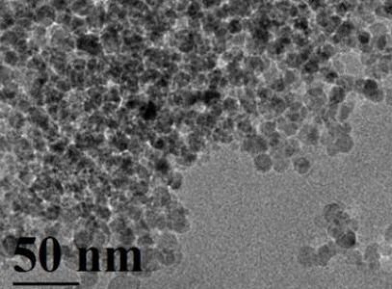
For the first time, researchers developed a three-dimensional dynamic model of an interaction between light and nanoparticles. They used a supercomputer with graphic accelerators for calculations. Results showed that silicon particles exposed to short intense laser pulses lose their symmetry temporarily. Their optical properties become strongly heterogeneous. Such a change in properties depends on particle size, therefore it can be used for light control in ultrafast information processing nanoscale devices. …
Improvement of computing devices today focuses on increasing information processing speeds. Nanophotonics is one of the sciences that can solve this problem by means of optical devices. Although optical signals can be transmitted and processed much faster than electronic ones, first, it is necessary to learn how to quickly control light on a small scale. For this purpose, one could use metal particles. They are efficient at localizing light, but weaken the signal, causing significant losses. However, dielectric and semiconducting materials, such as silicon, can be used instead of metal.
Silicon nanoparticles are now actively studied by researchers all around the world, including those at ITMO University. The long-term goal of such studies is to create ultrafast, compact optical signal modulators. They can serve as a basis for computers of the future. However, this technology will become feasible only once we understand how nanoparticles interact with light.
Silicon nanoparticles
“When a laser pulse hits the particle, a lot of free electrons are formed inside,” explains Sergey Makarov, head of ITMO’s Laboratory of Hybrid Nanophotonics and Optoelectronics. “A region saturated with oppositely charged particles is created. It is usually called electron-hole plasma. Plasma changes optical properties of particles and, up until today, it was believed that it spreads over the whole particle simultaneously, so that the particle’s symmetry is preserved. We demonstrated that this is not entirely true and an even distribution of plasma inside particles is not the only possible scenario.”
Scientists found that the electromagnetic field caused by an interaction between light and particles has a more complex structure. This leads to a light distortion which varies with time. Therefore, the symmetry of particles is disturbed and optical properties become different throughout one particle.
“Using analytical and numerical methods, we were the first to look inside the particle and we proved that the processes taking place there are far more complicated than we thought,” says Konstantin Ladutenko, staff member of ITMO’s International Research Center of Nanophotonics and Metamaterials. “Moreover, we found that by changing the particle size, we can affect its interaction with the light signal. This means we might be able to predict the signal path in an entire system of nanoparticles.”
In order to create a tool to study processes inside nanoparticles, scientists from ITMO University joined forces with colleagues from Jean Monnet University in France.
Sergey Makarov
“We developed analytical methods to determine the size range of the particles and their refractive index which would make a change in optical properties likely. Afterwards, we used powerful computational methods to monitor processes inside particles. Our colleagues performed calculations on a computer with graphics accelerators. Such computers are often used for cryptocurrency mining [emphasis mine]. However, we decided to enrich humanity with new knowledge, rather than enrich ourselves. Besides, bitcoin rate had just started to go down then,” adds Konstantin.
Devices based on these nanoparticles may become basic elements of optical computers, just as transistors are basic elements of electronics today. They will make it possible to distribute and redirect or branch the signal.
“Such asymmetric structures have a variety of applications, but we are focusing on ultra-fast signal processing,” continues Sergey. “We now have a powerful theoretical tool which will help us develop light management systems that will operate on a small scale – in terms of both time and space”.
Here’s a little more about ITMO University from its Wikipedia entry (Note: Links have been removed),
ITMO University (Russian: Университет ИТМО) is a large state university in Saint Petersburg and is one of Russia’s National Research Universities.[1] ITMO University is one of 15 Russian universities that were selected to participate in Russian Academic Excellence Project 5-100[2] by the government of the Russian Federation to improve their international competitiveness among the world’s leading research and educational centers.[3]
The ornate Chrysina resplendens beetle has a metallic gold colour. Image courtesy of K Robacker.
I haven’t read this yet but I’m willing to bet that the reason Central American jewel scarab beetles look like gold is due to nanoscale structures on their exoskeletons. Let’s see if I’m right, eh? From a June 15, 2017 news item on ScienceDaily,
The secrets of why central-American jewel scarab beetles look like they are made from pure gold, has been uncovered by physicists at the University of Exeter.
The ornate beetles, which have a brilliant metallic gold colour, are highly valued by collectors. But until now the reasons behind their golden iridescent hue, have not been fully understood.
University of Exeter physicists specialising in colour and light have done experiments exploring the origin of the scarab beetles’ striking metallic golden appearance, showing that the golden beetles have a unique ‘optical signature’. The structure of the beetle and its armour uniquely manipulates the way the light is reflected so that it looks like pure gold.
Professor Pete Vukusic, a physicist specialising in light and colour, led the research which involved experiments and advanced modelling. He found that the golden appearance is due to the high reflectiveness of the beetles’ exoskeleton, which also manipulates a property of the light called its polarisation: the orientation of the reflected light wave’s oscillations.
The scientists mapped the optical signature of the beetle’s Chrysina resplendens’ colour, and found it was unusually ‘optically-ambidextrous’, meaning that it reflects both left-handed and right-handed circularly-polarised light.
Professor Vukusic said: “The brilliant golden colour and distinctive polarised reflection from the scarab beetle Chrysina resplendens sets it completely apart from the hundreds of thousands of other beautiful and brightly coloured animals and plants across the natural world. Its exoskeleton has a bright, golden appearance that reflects both right-handed and left-handed circularly-polarised light simultaneously. This characteristic of Chrysina resplendens appears to be an exceptional and wonderfully specialised characteristic in currently known animals and plants. It will serve as a valuable platform from which bio-inspired optical technologies can spring. ”
The golden jewel beetle is prized by collectors because of its resemblance to the precious metal.
Other scarab beetles, valued by ancient cultures such as the Egyptians for use as amulets which were sometimes wrapped in the bandages of mummies, are jewel-like green and blue colours. The vast majority of brightly-coloured beetles tend to be green and do not reflect polarised light. These beetles, in comparison to the brilliant golden colour of Chrysina resplendens, lack much more specialised aspects of their exoskeleton’s finely detailed structure.
Dr Ewan Finlayson, research fellow on the project, said: “We were drawn to the study of this jewel scarab not only by its striking metallic golden appearance, but also by its ability to control a less obvious property of the reflected light: the polarisation. We have learned that there is great subtlety and detail to be found in these optical ‘signatures’ and in the elaborate natural structures that generate them.”
The golden jewel scarab beetle Chrysina resplendens, mainly found in the Americas, has evolved an exoskeleton that contains intricate nano-structures that are responsible for its appearance.
The spacing of the repeating layers of the nano-structures [emphasis mine] is found to vary over a specific range through the exoskeleton – a key property that causes the simultaneous reflection of a range of visible colours. It is this fact that explains the very bright reflection as well as the golden hue.
The nano-structured exoskeleton is composed of natural materials including chitin and various proteins. In addition to their brilliant reflectiveness, these structures are remarkable in the way they manipulate the way polarised light is reflected.
Their nanostructures produce circularly-polarised light, where the orientation of the light’s oscillations rotate as the light travels. The two possible directions of rotation are referred to as left handed and right handed.
The experiments build on the work of an early American scientist called Michelson [Albert A. Michelson] who, in 1911, looked at the polarised reflection from many different Chrysina beetles, and on the work of Anthony Neville (then at Bristol University) in 1971, who began looking more closely at Chrysina resplendens.
There are around 100 species of Chrysina jewel scarab, which are found exclusively in the New World, mostly in Mexico and Central America. The species Chrysina resplendens is found in Panama and Costa Rica. Chrysina scarabs typically live in mountain forests. The larvae feed on rotting logs of various tree species, while the adults feed on foliage. The larval form lasts for several months to a year, and pupation takes a month or two. After the adult emerges it lives for about a further three months, although this span probably varies between species.
One explanation for the highly-reflective appearance of the beetle exoskeleton is crypsis: the ability of the animal to blend in to its surroundings.
Dr Martin Stevens, Associate Professor of Sensory and Evolutionary Ecology at the University of Exeter and an expert in animal vision, colour change and camouflage, said:
“It is not absolutely clear why these beetles are a bright golden colour, but one option is that it somehow works in camouflage under some light conditions. The shiny golden colour could also change how the beetle is seen as it moves, potentially dazzling a would-be predator. There are many species which are iridescent but jewel beetles are one of the most charismatic and brightly coloured, and their colour might be used in mating. However, it is not clear how other beetles see the gold colour and reflected light. Many small mammals would not be able to distinguish the golden colour from reds, greens, and yellows, but a predatory bird would likely be able to see these colours well.”
An artificial blood vessel network that could lead the way to regenerating biologically-based blood vessel networks has been printed in 3D at the University of California at San Diego (UCSD) according to a March 2, 2017 news item on ScienceDaily,
Nanoengineers at the University of California San Diego have 3D printed a lifelike, functional blood vessel network that could pave the way toward artificial organs and regenerative therapies.
The new research, led by nanoengineering professor Shaochen Chen, addresses one of the biggest challenges in tissue engineering: creating lifelike tissues and organs with functioning vasculature — networks of blood vessels that can transport blood, nutrients, waste and other biological materials — and do so safely when implanted inside the body.
Researchers from other labs have used different 3D printing technologies to create artificial blood vessels. But existing technologies are slow, costly and mainly produce simple structures, such as a single blood vessel — a tube, basically. These blood vessels also are not capable of integrating with the body’s own vascular system.
“Almost all tissues and organs need blood vessels to survive and work properly. This is a big bottleneck in making organ transplants, which are in high demand but in short supply,” said Chen, who leads the Nanobiomaterials, Bioprinting, and Tissue Engineering Lab at UC San Diego. “3D bioprinting organs can help bridge this gap, and our lab has taken a big step toward that goal.”
Chen’s lab has 3D printed a vasculature network that can safely integrate with the body’s own network to circulate blood. These blood vessels branch out into many series of smaller vessels, similar to the blood vessel structures found in the body. The work was published in Biomaterials.
Chen’s team developed an innovative bioprinting technology, using their own homemade 3D printers, to rapidly produce intricate 3D microstructures that mimic the sophisticated designs and functions of biological tissues. Chen’s lab has used this technology in the past to create liver tissue and microscopic fish that can swim in the body to detect and remove toxins.
Researchers first create a 3D model of the biological structure on a computer. The computer then transfers 2D snapshots of the model to millions of microscopic-sized mirrors, which are each digitally controlled to project patterns of UV light in the form of these snapshots. The UV patterns are shined onto a solution containing live cells and light-sensitive polymers that solidify upon exposure to UV light. The structure is rapidly printed one layer at a time, in a continuous fashion, creating a 3D solid polymer scaffold encapsulating live cells that will grow and become biological tissue.
“We can directly print detailed microvasculature structures in extremely high resolution. Other 3D printing technologies produce the equivalent of ‘pixelated’ structures in comparison and usually require sacrificial materials and additional steps to create the vessels,” said Wei Zhu, a postdoctoral scholar in Chen’s lab and a lead researcher on the project.
And this entire process takes just a few seconds — a vast improvement over competing bioprinting methods, which normally take hours just to print simple structures. The process also uses materials that are inexpensive and biocompatible.
Chen’s team used medical imaging to create a digital pattern of a blood vessel network found in the body. Using their technology, they printed a structure containing endothelial cells, which are cells that form the inner lining of blood vessels.
The entire structure fits onto a small area measuring 4 millimeters × 5 millimeters, 600 micrometers thick (as thick as a stack containing 12 strands of human hair).
Researchers cultured several structures in vitro for one day, then grafted the resulting tissues into skin wounds of mice. After two weeks, the researchers examined the implants and found that they had successfully grown into and merged with the host blood vessel network, allowing blood to circulate normally.
Chen noted that the implanted blood vessels are not yet capable of other functions, such as transporting nutrients and waste. “We still have a lot of work to do to improve these materials. This is a promising step toward the future of tissue regeneration and repair,” he said.
Moving forward, Chen and his team are working on building patient-specific tissues using human induced pluripotent stem cells, which would prevent transplants from being attacked by a patient’s immune system. And since these cells are derived from a patient’s skin cells, researchers won’t need to extract any cells from inside the body to build new tissue. The team’s ultimate goal is to move their work to clinical trials. “It will take at least several years before we reach that goal,” Chen said.
This research upends centuries of scientific thought according to a Nov. 10, 2016 news item on ScienceDaily,
For centuries, scientists believed that light, like all waves, couldn’t be focused down smaller than its wavelength, just under a millionth of a metre. Now, researchers led by the University of Cambridge have created the world’s smallest magnifying glass, which focuses light a billion times more tightly, down to the scale of single atoms.
If they’ve created is a ‘magnifying glass’ as they call it in the news item, then I suppose you could call the ‘pico-cavity’ mentioned in the following press release, a lens.
In collaboration with European colleagues, the team used highly conductive gold nanoparticles to make the world’s tiniest optical cavity, so small that only a single molecule can fit within it. The cavity – called a ‘pico-cavity’ by the researchers – consists of a bump in a gold nanostructure the size of a single atom, and confines light to less than a billionth of a metre. The results, reported in the journal Science, open up new ways to study the interaction of light and matter, including the possibility of making the molecules in the cavity undergo new sorts of chemical reactions, which could enable the development of entirely new types of sensors.
According to the researchers, building nanostructures with single atom control was extremely challenging. “We had to cool our samples to -260°C in order to freeze the scurrying gold atoms,” said Felix Benz, lead author of the study. The researchers shone laser light on the sample to build the pico-cavities, allowing them to watch single atom movement in real time.
“Our models suggested that individual atoms sticking out might act as tiny lightning rods, but focusing light instead of electricity,” said Professor Javier Aizpurua from the Center for Materials Physics in San Sebastian in Spain, who led the theoretical section of this work.
“Even single gold atoms behave just like tiny metallic ball bearings in our experiments, with conducting electrons roaming around, which is very different from their quantum life where electrons are bound to their nucleus,” said Professor Jeremy Baumberg of the NanoPhotonics Centre at Cambridge’s Cavendish Laboratory, who led the research.
The findings have the potential to open a whole new field of light-catalysed chemical reactions, allowing complex molecules to be built from smaller components. Additionally, there is the possibility of new opto-mechanical data storage devices, allowing information to be written and read by light and stored in the form of molecular vibrations.
Here’s a link to and a citation for the paper,
Single-molecule optomechanics in “picocavities” by Felix Benz, Mikolaj K. Schmidt, Alexander Dreismann, Rohit Chikkaraddy, Yao Zhang, Angela Demetriadou, Cloudy Carnegie, Hamid Ohadi, Bart de Nijs, Ruben Esteban, Javier Aizpurua, Jeremy J. Baumberg. Science 11 Nov 2016: Vol. 354, Issue 6313, pp. 726-729 DOI: 10.1126/science.aah5243
The extraordinary effort to colonize our brains continues apace with a new sensor from Vanderbilt University. From an Oct. 27, 2016 news item on ScienceDaily,
A new kind of bioluminescent sensor causes individual brain cells to imitate fireflies and glow in the dark.
The probe, which was developed by a team of Vanderbilt scientists, is a genetically modified form of luciferase, the enzyme that a number of other species including fireflies use to produce light. …
The scientists created the technique as a new and improved method for tracking the interactions within large neural networks in the brain.
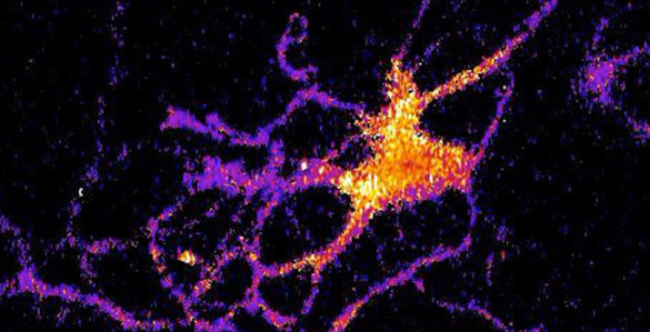
“For a long time neuroscientists relied on electrical techniques for recording the activity of neurons. These are very good at monitoring individual neurons but are limited to small numbers of neurons. The new wave is to use optical techniques to record the activity of hundreds of neurons at the same time,” said Carl Johnson, Stevenson Professor of Biological Sciences, who headed the effort.
Individual neuron glowing with bioluminescent light produced by a new genetically engineered sensor. (Johnson Lab / Vanderbilt University)
“Most of the efforts in optical recording use fluorescence, but this requires a strong external light source which can cause the tissue to heat up and can interfere with some biological processes, particularly those that are light sensitive,” he [Carl Johnson] said.
Based on their research on bioluminescence in “a scummy little organism, the green alga Chlamydomonas, that nobody cares much about” Johnson and his colleagues realized that if they could combine luminescence with optogenetics – a new biological technique that uses light to control cells, particularly neurons, in living tissue – they could create a powerful new tool for studying brain activity.
“There is an inherent conflict between fluorescent techniques and optogenetics. The light required to produce the fluorescence interferes with the light required to control the cells,” said Johnson. “Luminescence, on the other hand, works in the dark!”
Johnson and his collaborators – Associate Professor Donna Webb, Research Assistant Professor Shuqun Shi, post-doctoral student Jie Yang and doctoral student Derrick Cumberbatch in biological sciences and Professor Danny Winder and postdoctoral student Samuel Centanni in molecular physiology and biophysics – genetically modified a type of luciferase obtained from a luminescent species of shrimp so that it would light up when exposed to calcium ions. Then they hijacked a virus that infects neurons and attached it to their sensor molecule so that the sensors are inserted into the cell interior.
The researchers picked calcium ions because they are involved in neuron activation. Although calcium levels are high in the surrounding area, normally they are very low inside the neurons. However, the internal calcium level spikes briefly when a neuron receives an impulse from one of its neighbors.
They tested their new calcium sensor with one of the optogenetic probes (channelrhodopsin) that causes the calcium ion channels in the neuron’s outer membrane to open, flooding the cell with calcium. Using neurons grown in culture they found that the luminescent enzyme reacted visibly to the influx of calcium produced when the probe was stimulated by brief light flashes of visible light.
To determine how well their sensor works with larger numbers of neurons, they inserted it into brain slices from the mouse hippocampus that contain thousands of neurons. In this case they flooded the slices with an increased concentration of potassium ions, which causes the cell’s ion channels to open. Again, they found that the sensor responded to the variations in calcium concentrations by brightening and dimming.
“We’ve shown that the approach works,” Johnson said. “Now we have to determine how sensitive it is. We have some indications that it is sensitive enough to detect the firing of individual neurons, but we have to run more tests to determine if it actually has this capability.”
Here’s a link to and a citation for the paper,
Coupling optogenetic stimulation with NanoLuc-based luminescence (BRET) Ca++ sensing by Jie Yang, Derrick Cumberbatch, Samuel Centanni, Shu-qun Shi, Danny Winder, Donna Webb, & Carl Hirschie Johnson. Nature Communications 7, Article number: 13268 (2016) doi:10.1038/ncomms13268 Published online: 27 October 2016
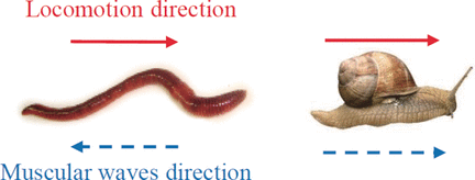
Directed motion seems simple to us, but the coordinated interplay of complex processes is needed, even for seemingly simple crawling motions of worms or snails. By using a gel that periodically swells and shrinks, researchers developed a model for the waves of muscular contraction and relaxation involved in crawling. As reported in the journal Angewandte Chemie, they were able to produce two types of crawling motion by using inhomogeneous irradiation.
Crawling comes from waves that travel through muscle. These waves can travel in the same direction as the animal is crawling (direct waves), from the tail end toward the head, or in the opposite direction (retrograde waves), from the head toward the tail. While land snails use the former type of wave, earthworms and limpets use the latter. Chitons (polyplacophora) can switch between both types of movement.
With the aid of a chemical model in the form of a self-oscillating gel, researchers working with Qingyu Gao at the China University of Mining and Technology (Jiangsu, China) and Irving R. Epstein at Brandeis University (Waltham, Massachusetts, USA) have been able to answer some of the many questions about these crawling processes.
A gel is a molecular network with liquid bound in the gaps. In this case, the liquid contains all of the ingredients needed for an oscillating chemical reaction (“chemical clock”). The researchers incorporated one component of their reaction system into the network: a ruthenium complex. During the reaction, the ruthenium periodically switches between two oxidation states, Ru2+ and Ru3+. This switch changes the gel so that in one state it can hold more liquid than the other, so the gel swells and shrinks periodically. Like the chemical clock, these regions propagate in waves, similar to the waves of muscle contractions in crawling.
The complex used in this gel also changes oxidation state when irradiated with light. When the right half of the gel is irradiated more strongly than the left, the waves move from right to left, i.e., from a high- to a low-frequency region of gel oscillations. Once the difference in intensity of irradiation reaches a certain threshold, it causes a wormlike motion of the gel from left to right, retrograde wave locomotion. If the difference is increased further, the gel comes to a stop. A further increase in the difference causes the gel to move again, but in the opposite direction, i.e., direct wave locomotion. The nonuniform illumination plays a role analogous to that of anchoring segments and appendages (such as limbs and wings) during cell migration and animal locomotion, which control the direction of locomotion by strengthening direct movement and/or inhibiting the opposite movement.
By using computational models, the researchers were able to describe these processes. Within the gel, there are regions where pulling forces predominate; pushing forces predominate in other areas. Variations in the intensity of the irradiation lead to different changes in the friction forces and the tensions in the gel. When these effects are added up, it is possible to predict in which direction a particular grid element of the gel will move.
One important finding from this model: special changes in the viscoelastic properties of the slime excreted by the snails and worms as they crawl are not required for locomotion, whether retrograde or direct.
For anyone curious about the song, there’s this from its Wikipedia entry (Note: Links have been removed),
“The Loco-Motion” is a 1962 pop song written by American songwriters Gerry Goffin and Carole King. “The Loco-Motion” was originally written for Dee Dee Sharp but Sharp turned the song down.[1] The song is notable for appearing in the American Top 5 three times – each time in a different decade, performed by artists from three different cultures: originally African American pop singer Little Eva in 1962 (U.S. No. 1);[2] then American band Grand Funk Railroad in 1974 (U.S. No. 1);[3] and finally Australian singer Kylie Minogue in 1988 (U.S. No. 3).[4]
The song is a popular and enduring example of the dance-song genre: much of the lyrics are devoted to a description of the dance itself, usually done as a type of line dance. However, the song came before the dance.
“The Loco-Motion” was also the second song to reach No. 1 by two different musical acts. The earlier song to do this was “Go Away Little Girl”, also written by Goffin and King. It is one of only nine songs to achieve this
I had not realized this song had such a storied past; there’s a lot more about it in the Wikipedia entry.