Great Pyramid of Giza and Sphinx [downloaded from http://news.ifmo.ru/en/science/photonics/news/7731/]
Russian and German scientists have taken a closer look at the Great Pyramid as they investigate better ways of designing sensors and solar cells. From a July 30, 2018 news item on Nanowerk,
An international research group applied methods of theoretical physics to investigate the electromagnetic response of the Great Pyramid to radio waves. Scientists predicted that under resonance conditions the pyramid can concentrate electromagnetic energy in its internal chambers and under the base. The research group plans to use these theoretical results to design nanoparticles capable of reproducing similar effects in the optical range. Such nanoparticles may be used, for example, to develop sensors and highly efficient solar cells.
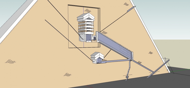
While Egyptian pyramids are surrounded by many myths and legends, we have little scientifically reliable information about their physical properties. As it turns out, sometimes this information proves to be more fascinating than any fiction. This idea found confirmation in a new joint study undertaken by scientists from ITMO University and the Laser Zentrum Hannover. The physicists took an interest in how the Great Pyramid would interact with electromagnetic waves of a proportional, or resonant, length. Calculations showed that in the resonant state the pyramid can concentrate electromagnetic energy in its internal chambers as well as under its base, where the third unfinished chamber is located.
These conclusions were derived on the basis of numerical modeling and analytical methods of physics. The researchers first estimated that resonances in the pyramid can be induced by radio waves with a length ranging from 200 to 600 meters. Then they made a model of the electromagnetic response of the pyramid and calculated the extinction cross section. This value helps to estimate which part of the incident wave energy can be scattered or absorbed by the pyramid under resonant conditions. Finally, for the same conditions, the scientists obtained the electromagnetic fields distribution inside the pyramid.
3D model of the pyramid. Credit: cheops.SU
In order to explain the results, the scientists conducted a multipole analysis. This method is widely used in physics to study the interaction between a complex object and electromagnetic field. The object scattering the field is replaced by a set of simpler sources of radiation: multipoles. The collection of multipoles radiation coincides with the field scattering by an entire object. Therefore, by knowing the type of each multipole, it is possible to predict and explain the distribution and configuration of the scattered fields in the whole system.
The Great Pyramid attracted the researchers’ attention while they were studying the interaction between light and dielectric nanoparticles. The scattering of light by nanoparticles depends on their size, shape, and refractive index of the source material. By varying these parameters, it is possible to determine the resonance scattering regimes and use them to develop devices for controlling light at the nanoscale.
“Egyptian pyramids have always attracted great attention. We as scientists were interested in them as well, and so we decided to look at the Great Pyramid as a particle resonantly dissipating radio waves. Due to the lack of information about the physical properties of the pyramid, we had to make some assumptions. For example, we assumed that there are no unknown cavities inside, and the building material has the properties of an ordinary limestone and is evenly distributed in and out of the pyramid. With these assumptions, we obtained interesting results that can have important practical applications,” says Andrey Evlyukhin, DSc, scientific supervisor and coordinator of the research.
Now the scientists plan to use the results to reproduce similar effects at the nanoscale.
Polina Kapitanova
“By choosing a material with suitable electromagnetic properties, we can obtain pyramidal nanoparticles with a potential for practical application in nanosensors and effective solar cells,” says Polina Kapitanova, PhD, associate at the Faculty of Physics and Engineering of ITMO University.
The research was supported by the Russian Science Foundation and the Deutsche Forschungsgemeinschaft (grants № 17-79-20379 and №16-12-10287).
This was not the mining hardware I expected and it enters the picture after this paragraph which has been excerpted from a February 28, 2018 news item on Nanowerk,
For the first time, researchers developed a three-dimensional dynamic model of an interaction between light and nanoparticles. They used a supercomputer with graphic accelerators for calculations. Results showed that silicon particles exposed to short intense laser pulses lose their symmetry temporarily. Their optical properties become strongly heterogeneous. Such a change in properties depends on particle size, therefore it can be used for light control in ultrafast information processing nanoscale devices. …
Improvement of computing devices today focuses on increasing information processing speeds. Nanophotonics is one of the sciences that can solve this problem by means of optical devices. Although optical signals can be transmitted and processed much faster than electronic ones, first, it is necessary to learn how to quickly control light on a small scale. For this purpose, one could use metal particles. They are efficient at localizing light, but weaken the signal, causing significant losses. However, dielectric and semiconducting materials, such as silicon, can be used instead of metal.
Silicon nanoparticles are now actively studied by researchers all around the world, including those at ITMO University. The long-term goal of such studies is to create ultrafast, compact optical signal modulators. They can serve as a basis for computers of the future. However, this technology will become feasible only once we understand how nanoparticles interact with light.
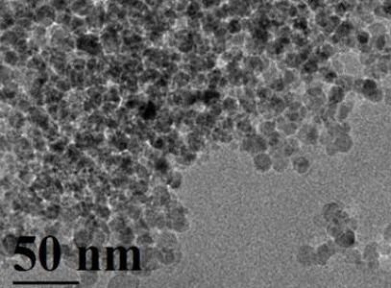
Silicon nanoparticles
“When a laser pulse hits the particle, a lot of free electrons are formed inside,” explains Sergey Makarov, head of ITMO’s Laboratory of Hybrid Nanophotonics and Optoelectronics. “A region saturated with oppositely charged particles is created. It is usually called electron-hole plasma. Plasma changes optical properties of particles and, up until today, it was believed that it spreads over the whole particle simultaneously, so that the particle’s symmetry is preserved. We demonstrated that this is not entirely true and an even distribution of plasma inside particles is not the only possible scenario.”
Scientists found that the electromagnetic field caused by an interaction between light and particles has a more complex structure. This leads to a light distortion which varies with time. Therefore, the symmetry of particles is disturbed and optical properties become different throughout one particle.
“Using analytical and numerical methods, we were the first to look inside the particle and we proved that the processes taking place there are far more complicated than we thought,” says Konstantin Ladutenko, staff member of ITMO’s International Research Center of Nanophotonics and Metamaterials. “Moreover, we found that by changing the particle size, we can affect its interaction with the light signal. This means we might be able to predict the signal path in an entire system of nanoparticles.”
In order to create a tool to study processes inside nanoparticles, scientists from ITMO University joined forces with colleagues from Jean Monnet University in France.
Sergey Makarov
“We developed analytical methods to determine the size range of the particles and their refractive index which would make a change in optical properties likely. Afterwards, we used powerful computational methods to monitor processes inside particles. Our colleagues performed calculations on a computer with graphics accelerators. Such computers are often used for cryptocurrency mining [emphasis mine]. However, we decided to enrich humanity with new knowledge, rather than enrich ourselves. Besides, bitcoin rate had just started to go down then,” adds Konstantin.
Devices based on these nanoparticles may become basic elements of optical computers, just as transistors are basic elements of electronics today. They will make it possible to distribute and redirect or branch the signal.
“Such asymmetric structures have a variety of applications, but we are focusing on ultra-fast signal processing,” continues Sergey. “We now have a powerful theoretical tool which will help us develop light management systems that will operate on a small scale – in terms of both time and space”.
Here’s a little more about ITMO University from its Wikipedia entry (Note: Links have been removed),
ITMO University (Russian: Университет ИТМО) is a large state university in Saint Petersburg and is one of Russia’s National Research Universities.[1] ITMO University is one of 15 Russian universities that were selected to participate in Russian Academic Excellence Project 5-100[2] by the government of the Russian Federation to improve their international competitiveness among the world’s leading research and educational centers.[3]
A Dec. 14, 2015 news item on Nanowerk announces a new ceramic firefighting foam developed in Russia,
A team of chemists from ITMO University, in collaboration with research company SOPOT, has developed a novel type of firefighting foam based on inorganic silica nanoparticles. The new foam beats existing analogues in fire extinguishing capacity, thermal and mechanical stability and biocompatibility.
Fighting large-scale fires usually involves firefighting foams based on synthetic substances, such as prefluorinated surfactants, that, despite their effectiveness, are extremely toxic for living organisms. Complete biodegradation of such foams can last for more than 200 years [emphasis mine], with residues quickly penetrating deep into soil and surface water. This leads to the the accumulation of toxic elements in living organisms, such as plants, animals and men. Many countries have declined the use of such fire extinguishing agents or opted for reducing the production of such substances despite the absence of any decent alternatives.
A group of scientists from the International Laboratory of Advanced Materials and Technologies (SCAMT) at ITMO University in Saint Petersburg and research company SOPOT devised a foam, which was awarded full biodegradability and whose fire extinguishing capacity is higher than that of any existing analogue currently in use by fire fighters. After the fire is extinguished, the substance actively absorbs water, softens and falls apart into bioinert silica particles. And even when the foam accidentally enters living organisms, it does not not pose any danger to them.
“Our foam is based on silica nanoparticles, which create a polymer network when exposed to air,” says Alexander Vinogradov, deputy head of the SCAMT laboratory. “Such a network embraces and adheres to the burning object and momentarily cools it down. At the same time, the foam itself hardens. The inorganic origin of this polymer network allows it to resist temperatures above 1000 degrees Celsius, which ensures gigantic stability from the aggressive environment in the midst of a raging fire.”
“Most existing foams are made of organic materials and quickly deteriorate when temperature approaches 300 degrees Celsius. In our case, the foam creates a hard frame that not only puts out the fire, but also protects the object from re-ignition. With ordinary foams, re-ignition occurs within seconds after flame is applied to the object again.”
The scientists conducted a series of large-scale experiments of the hardening foam, including the imitation of an actual forest fire. The foam was used to create a flame retardant belt that was supposed stop the spread of the fire. The tests demonstrated that the foam easily localizes the forest fire seat and can stay active during the whole fire season.
“The flame retardant belt made of our foam will prevent the spread of any forest fire, regardless of its strength and level of complexity,” says Gennady Kuprin, head of SOPOT. “We can localize the fire and be sure that the adjacent territories will be safe. This is crucial to organize evacuation works during forest fires, where 9 of 10 people die in our and other countries.”
The standard firefighting foam can take up to 200 years before completely degrading? I hope this new foam is all they say it is and that they can get it to market. In the meantime, here’s a link to and a citation for the researchers’ paper,
Silica foams for fire prevention and firefighting by Alexander V. Vinogradov, Denis Kuprin, Iosif Abduragimov, Gennadii Kuprin, Evgeniy Serebriyakov, and Vladimir V. Vinogradov. ACS Appl. Mater. Interfaces, DOI: 10.1021/acsami.5b08653
Publication Date (Web): October 22, 2015
“NPO Sopot” was founded in 1994 in St. Petersburg. Its creation was preceded by many years of scientific research and experimental design work done in person at the head of the firm basis of the Ministry of Defence and the Ministry of Internal Affairs of Russia, as well as, with the participation and cooperation with representatives of several institutions of the defense industry (the Sukhoi Design Bureau, Institute TRANSMASH, Academy. Zhukovsky etc.), the Ministry of Civil aviation, Fire Prevention Russian Interior Ministry, the Russian Interior Ministry VIPTSH
General Director of JSC “NPO” Sopot “Gennady Kuprin. Winner of the National Industry Award” Bison-2006 “, the grand prize Emergencies Ministry in 2005 and 2006., Awarded the” Golden Shield of the Russian economy, “international diploma” European quality “member of the International Academy of Patronage, the World Academy of Integrated Security.
Even after all these years, nano stuff can seem magical to me. Russian researchers according to a Sept. 8, 2015 news item on Nanotechnology Now have already developed a prototype of a transistor based on a single silicon nanoparticle,
Physicists from the Department of Nanophotonics and Metamaterials at ITMO University have experimentally demonstrated the feasibility of designing an optical analog of a transistor based on a single silicon nanoparticle. Because transistors are some of the most fundamental components of computing circuits, the results of the study have crucial importance for the development of optical computers, where transistors must be very small and ultrafast at the same time. …
A Sept. 7, 2015 ITMO University press release on EurekAlert, which originated the news item, describes the problem the researchers were grappling with and their proposed solution,
The performance of modern computers, which use electrons as signal carriers, is largely limited by the time needed to trigger the transistor – usually around 0.1 – 1 nanoseconds (1/1.000.000.000 of a second). Next-generation optical computers, however, rely on photons to carry the useful signal, which heavily increases the amount of information passing through the transistor per second. For this reason, the creation of an ultrafast and compact all-optical transistor is considered to be instrumental in the development of optical computing. Such a nanodevice would enable scientists to control the propagation of an optical signal beam by means of an external control beam within several picoseconds (1/1.000.000.000.000 of a second).
In the study, a group of Russian scientists from ITMO University, Lebedev Physical Institute and Academic University in Saint Petersburg put forward a completely new approach to design such optical transistors, having made a prototype using only one silicon nanoparticle.
The scientists found that they can dramatically change the properties of a silicon nanoparticle by irradiating it with intense and ultrashort laser pulse. The laser thus acts as a control beam, providing ultrafast photoexcitation of dense and rapidly recombining electron-hole plasma whose presence changes the dielectric permittivity of silicon for a few picoseconds. This abrupt change in the optical properties of the nanoparticle opens the possibility to control the direction, in which incident light is scattered. For instance, the direction of nanoparticle scattering can be changed from backward to forward on picoseconds timescale, depending on the intensity of the incident control laser pulse. This concept of ultrafast switching is very promising for designing of all-optical transistor.
“Generally, researchers in this field are focused on designing nanoscale all-optical transistors by means of controlling the absorption of nanoparticles, which, in essence, is entirely logical. In high absorption mode, the light signal is absorbed by the nanoparticle and cannot pass through, while out of this mode the light is allowed to propagate past the nanoparticle. However, this method did not yield any decisive results,” explains Sergey Makarov, lead author of the study and senior researcher at the Department of Nanophotonics and Metamaterials. “Our idea is different in the sense that we control not the absorption properties of the nanoparticle, but rather its scattering diagram. Let’s say, the nanoparticle normally scatters almost all incident light in the backward direction, but once we irradiate it by a control pulse, it becomes reconfigured and starts scattering light forward.”
The choice of silicon as a material for the optical transistor was not accidental. Creating an optical transistor requires the use of inexpensive materials appropriate for mass production and capable of changing their optical properties in several picoseconds (in the regime of dense electron-hole plasma) without getting overheated at the same time.
“The time it takes us to deactivate our nanoparticle amounts to just several picoseconds, while to activate it we need no more than tens of femtoseconds (1/1.000.000.000.000.000). Now we already have experimental data that clearly indicates that a single silicon nanoparticle can indeed play the role of an all-optical transistor. Currently we are planning to conduct new experiments, where, along with a laser control beam, we will introduce a useful signal beam”, concludes Pavel Belov, coauthor of the paper and head of the Department of Nanophotonics and Metamaterials.