This was not the mining hardware I expected and it enters the picture after this paragraph which has been excerpted from a February 28, 2018 news item on Nanowerk,
For the first time, researchers developed a three-dimensional dynamic model of an interaction between light and nanoparticles. They used a supercomputer with graphic accelerators for calculations. Results showed that silicon particles exposed to short intense laser pulses lose their symmetry temporarily. Their optical properties become strongly heterogeneous. Such a change in properties depends on particle size, therefore it can be used for light control in ultrafast information processing nanoscale devices. …
Improvement of computing devices today focuses on increasing information processing speeds. Nanophotonics is one of the sciences that can solve this problem by means of optical devices. Although optical signals can be transmitted and processed much faster than electronic ones, first, it is necessary to learn how to quickly control light on a small scale. For this purpose, one could use metal particles. They are efficient at localizing light, but weaken the signal, causing significant losses. However, dielectric and semiconducting materials, such as silicon, can be used instead of metal.
Silicon nanoparticles are now actively studied by researchers all around the world, including those at ITMO University. The long-term goal of such studies is to create ultrafast, compact optical signal modulators. They can serve as a basis for computers of the future. However, this technology will become feasible only once we understand how nanoparticles interact with light.
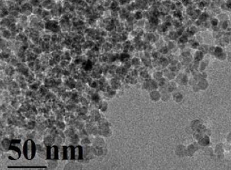
Silicon nanoparticles
“When a laser pulse hits the particle, a lot of free electrons are formed inside,” explains Sergey Makarov, head of ITMO’s Laboratory of Hybrid Nanophotonics and Optoelectronics. “A region saturated with oppositely charged particles is created. It is usually called electron-hole plasma. Plasma changes optical properties of particles and, up until today, it was believed that it spreads over the whole particle simultaneously, so that the particle’s symmetry is preserved. We demonstrated that this is not entirely true and an even distribution of plasma inside particles is not the only possible scenario.”
Scientists found that the electromagnetic field caused by an interaction between light and particles has a more complex structure. This leads to a light distortion which varies with time. Therefore, the symmetry of particles is disturbed and optical properties become different throughout one particle.
“Using analytical and numerical methods, we were the first to look inside the particle and we proved that the processes taking place there are far more complicated than we thought,” says Konstantin Ladutenko, staff member of ITMO’s International Research Center of Nanophotonics and Metamaterials. “Moreover, we found that by changing the particle size, we can affect its interaction with the light signal. This means we might be able to predict the signal path in an entire system of nanoparticles.”
In order to create a tool to study processes inside nanoparticles, scientists from ITMO University joined forces with colleagues from Jean Monnet University in France.
Sergey Makarov
“We developed analytical methods to determine the size range of the particles and their refractive index which would make a change in optical properties likely. Afterwards, we used powerful computational methods to monitor processes inside particles. Our colleagues performed calculations on a computer with graphics accelerators. Such computers are often used for cryptocurrency mining [emphasis mine]. However, we decided to enrich humanity with new knowledge, rather than enrich ourselves. Besides, bitcoin rate had just started to go down then,” adds Konstantin.
Devices based on these nanoparticles may become basic elements of optical computers, just as transistors are basic elements of electronics today. They will make it possible to distribute and redirect or branch the signal.
“Such asymmetric structures have a variety of applications, but we are focusing on ultra-fast signal processing,” continues Sergey. “We now have a powerful theoretical tool which will help us develop light management systems that will operate on a small scale – in terms of both time and space”.
Here’s a little more about ITMO University from its Wikipedia entry (Note: Links have been removed),
ITMO University (Russian: Университет ИТМО) is a large state university in Saint Petersburg and is one of Russia’s National Research Universities.[1] ITMO University is one of 15 Russian universities that were selected to participate in Russian Academic Excellence Project 5-100[2] by the government of the Russian Federation to improve their international competitiveness among the world’s leading research and educational centers.[3]
Even after all these years, nano stuff can seem magical to me. Russian researchers according to a Sept. 8, 2015 news item on Nanotechnology Now have already developed a prototype of a transistor based on a single silicon nanoparticle,
Physicists from the Department of Nanophotonics and Metamaterials at ITMO University have experimentally demonstrated the feasibility of designing an optical analog of a transistor based on a single silicon nanoparticle. Because transistors are some of the most fundamental components of computing circuits, the results of the study have crucial importance for the development of optical computers, where transistors must be very small and ultrafast at the same time. …
A Sept. 7, 2015 ITMO University press release on EurekAlert, which originated the news item, describes the problem the researchers were grappling with and their proposed solution,
The performance of modern computers, which use electrons as signal carriers, is largely limited by the time needed to trigger the transistor – usually around 0.1 – 1 nanoseconds (1/1.000.000.000 of a second). Next-generation optical computers, however, rely on photons to carry the useful signal, which heavily increases the amount of information passing through the transistor per second. For this reason, the creation of an ultrafast and compact all-optical transistor is considered to be instrumental in the development of optical computing. Such a nanodevice would enable scientists to control the propagation of an optical signal beam by means of an external control beam within several picoseconds (1/1.000.000.000.000 of a second).
In the study, a group of Russian scientists from ITMO University, Lebedev Physical Institute and Academic University in Saint Petersburg put forward a completely new approach to design such optical transistors, having made a prototype using only one silicon nanoparticle.
The scientists found that they can dramatically change the properties of a silicon nanoparticle by irradiating it with intense and ultrashort laser pulse. The laser thus acts as a control beam, providing ultrafast photoexcitation of dense and rapidly recombining electron-hole plasma whose presence changes the dielectric permittivity of silicon for a few picoseconds. This abrupt change in the optical properties of the nanoparticle opens the possibility to control the direction, in which incident light is scattered. For instance, the direction of nanoparticle scattering can be changed from backward to forward on picoseconds timescale, depending on the intensity of the incident control laser pulse. This concept of ultrafast switching is very promising for designing of all-optical transistor.
“Generally, researchers in this field are focused on designing nanoscale all-optical transistors by means of controlling the absorption of nanoparticles, which, in essence, is entirely logical. In high absorption mode, the light signal is absorbed by the nanoparticle and cannot pass through, while out of this mode the light is allowed to propagate past the nanoparticle. However, this method did not yield any decisive results,” explains Sergey Makarov, lead author of the study and senior researcher at the Department of Nanophotonics and Metamaterials. “Our idea is different in the sense that we control not the absorption properties of the nanoparticle, but rather its scattering diagram. Let’s say, the nanoparticle normally scatters almost all incident light in the backward direction, but once we irradiate it by a control pulse, it becomes reconfigured and starts scattering light forward.”
The choice of silicon as a material for the optical transistor was not accidental. Creating an optical transistor requires the use of inexpensive materials appropriate for mass production and capable of changing their optical properties in several picoseconds (in the regime of dense electron-hole plasma) without getting overheated at the same time.
“The time it takes us to deactivate our nanoparticle amounts to just several picoseconds, while to activate it we need no more than tens of femtoseconds (1/1.000.000.000.000.000). Now we already have experimental data that clearly indicates that a single silicon nanoparticle can indeed play the role of an all-optical transistor. Currently we are planning to conduct new experiments, where, along with a laser control beam, we will introduce a useful signal beam”, concludes Pavel Belov, coauthor of the paper and head of the Department of Nanophotonics and Metamaterials.