Tag Archives: TU Wien

Key to quantum electronics could be germanium-bonded aluminium

I have not seen aluminum called aluminium in quite some time. (I’ve always had a fondness for that extra syllable.) I first saw notice of this work from Austria in an October 11, 2021 news item on Nanowerk,

A novel electronic component from TU Wien (Vienna) could be an important key to the era of quantum information technology: Using a special manufacturing process, pure germanium is bonded with aluminium in a way that atomically sharp interfaces are created. This results in a so-called monolithic metal-semiconductor-metal heterostructure.

This structure shows unique effects that are particularly evident at low temperatures. The aluminium becomes superconducting – but not only that, this property is also transferred to the adjacent germanium semiconductor and can be specifically controlled with electric fields. This makes it excellently suited for complex applications in quantum technology, such as processing quantum bits.

A particular advantage is that using this approach, it is not necessary to develop completely new technologies. Instead, mature and well established semiconductor fabrication techniqueses can be used to enable germanium-based quantum electronics.

An October 6, 2021 Technical University of Vienna (TU Wien) press release (also on EurekAlert but published October 12, 2021), which originated the news item, delves into the technical details and the importance of temperature,

Germanium: difficult to form high-quality contacts

“Germanium is a material which will definitely play an important role in semiconductor technology for the development of faster and more energy-efficient components,” says Dr. Masiar Sistani from the Institute for Solid State Electronics at TU Wien. However, if it is used to produce components on a nanometre scale, major problems arise: the material makes it extremely difficult to produce high-quality electrical contacts. This is related to the high impact of even smallest impurities at the contact points that significantly alter the electrical properties. “We have therefore set ourselves the task of developing a new manufacturing method that enables reliable and reproducible contact properties”, says Masiar Sistani.

Diffusing atoms

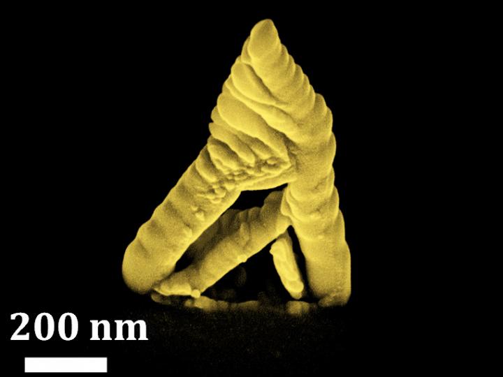
The key is temperature: when nanometre-structured germanium and aluminium are brought into contact and heated, the atoms of both materials begin to diffuse into the neighbouring material – but to very different extents: the germanium atoms move rapidly into the aluminium, whereas aluminium hardly diffuses into the germanium at all. “Thus, if you connect two aluminium contacts to a thin germanium nanowire and raise the temperature to 350 degrees Celsius, the germanium atoms diffuse off the edge of the nanowire. This creates empty spaces into which the aluminium can then easily penetrate,” explains Masiar Sistani. “In the end, only a few nanometre area in the middle of the nanowire consists of germanium, the rest has been filled up by aluminium.”

Normally, aluminium is made up of tiny crystal grains, but this novel fabrication method forms a perfect single crystal in which the aluminium atoms are arranged in a uniform pattern. As can be seen under the transmission electron microscope, a perfectly clean and atomically sharp transition is formed between germanium and aluminium, with no disordered region in between. In contrast to conventional methods where electrical contacts are applied to a semiconductor, for example by evaporating a metal, no oxides can form at the boundary layer.

Quantum transport in Grenoble

In order to take a closer look at the properties of this monolithic metal-semiconductor heterostructure of germanium and aluminium at low temperature, we collaborated with Dr. Olivier Buisson and Dr. Cécile Naud from the quantum electronics circuits group at Néel Institute – CNRS-UGA [Centre National de la Recherche Scientifique; Université Grenoble Alpes] in Grenoble. It turned out that the novel structure indeed has quite remarkable properties: “Not only were we able to demonstrate superconductivity in pure, undoped germanium for the first time, we were also able to show that this structure can be switched between quite different operating states using electric fields. Such a germanium quantum dot device can not only be superconducting but also completely insulating, or it can behave like a Josephson transistor, an important basic element of quantum electronic circuits,” explains Masiar Sistani.

This new heterostructure combines a whole range of advantages: The structure has excellent physical properties needed for quantum technologies, such as high carrier mobility and excellent manipulability with electric fields, and it has the additional advantage of fitting well with already established microelectronics technologies: Germanium is already used in current chip architectures and the temperatures required for heterostructure formation are compatible with well-established semiconductor processing schemes. The novel structures not only have theoretically interesting quantum properties, but also opens up a technologically very realistic possibility of enabling further novel and energy-saving devices.

Here’s a link to and a citation for the paper,

Al–Ge–Al Nanowire Heterostructure: From Single-Hole Quantum Dot to Josephson Effect by Jovian Delaforce, Masiar Sistani, Roman B. G. Kramer, Minh A. Luong, Nicolas Roch, Walter M. Weber, Martien I. den Hertog, Eric Robin, Cecile Naud, Alois Lugstein, Olivier Buisson. Advanced Materials Volume 33, Issue 39 October 1, 2021 2101989 DOI: https://doi.org/10.1002/adma.202101989 First published [online]: 08 August 2021

This paper is behind a paywall.

Using sound to transfer quantum information

It seems sound is becoming more prominent as a means of science data communication (data sonification) and in this upcoming case, data transfer. From a June 5, 2018 news item on ScienceDaily,

Quantum physics is on the brink of a technological breakthrough: new types of sensors, secure data transmission methods and maybe even computers could be made possible thanks to quantum technologies. However, the main obstacle here is finding the right way to couple and precisely control a sufficient number of quantum systems (for example, individual atoms).

A team of researchers from TU Wien and Harvard University has found a new way to transfer the necessary quantum information. They propose using tiny mechanical vibrations. The atoms are coupled with each other by ‘phonons’ — the smallest quantum mechanical units of vibrations or sound waves.

A June 5, 2018 Technical University of Vienna (TU Wien) press release, which originated the news item, explains the work in greater detail,

“We are testing tiny diamonds with built-in silicon atoms – these quantum systems are particularly promising,” says Professor Peter Rabl from TU Wien. “Normally, diamonds are made exclusively of carbon, but adding silicon atoms in certain places creates defects in the crystal lattice where quantum information can be stored.” These microscopic flaws in the crystal lattice can be used like a tiny switch that can be switched between a state of higher energy and a state of lower energy using microwaves.

Together with a team from Harvard University, Peter Rabl’s research group has developed a new idea to achieve the targeted coupling of these quantum memories within the diamond. One by one they can be built into a tiny diamond rod measuring only a few micrometres in length, like individual pearls on a necklace. Just like a tuning fork, this rod can then be made to vibrate – however, these vibrations are so small that they can only be described using quantum theory. It is through these vibrations that the silicon atoms can form a quantum-mechanical link to each other.

“Light is made from photons, the quantum of light. In the same way, mechanical vibrations or sound waves can also be described in a quantum-mechanical manner. They are comprised of phonons – the smallest possible units of mechanical vibration,” explains Peter Rabl. As the research team has now been able to show using simulation calculations, any number of these quantum memories can be linked together in the diamond rod thanks to these phonons. The individual silicon atoms are “switched on and off” using microwaves. During this process, they emit or absorb phonons. This creates a quantum entanglement of different silicon defects, thus allowing quantum information to be transferred.

The road to a scalable quantum network
Until now it was not clear whether something like this was even possible: “Usually you would expect the phonons to be absorbed somewhere, or to come into contact with the environment and thus lose their quantum mechanical properties,” says Peter Rabl. “Phonons are the enemy of quantum information, so to speak. But with our calculations, we were able to show that, when controlled appropriately using microwaves, the phonons are in fact useable for technical applications.”

The main advantage of this new technology lies in its scalability: “There are many ideas for quantum systems that, in principle, can be used for technological applications. The biggest problem is that it is very difficult to connect enough of them to be able to carry out complicated computing operations,” says Peter Rabl. The new strategy of using phonons for this purpose could pave the way to a scalable quantum technology.

Here’s a link to and a citation for the paper,

Phonon Networks with Silicon-Vacancy Centers in Diamond Waveguides by M.-A. Lemonde, S. Meesala, A. Sipahigil, M. J. A. Schuetz, M. D. Lukin, M. Loncar, and P. Rabl. Phys. Rev. Lett. 120 (21), 213603 DOI:https://doi.org/10.1103/PhysRevLett.120.213603 Published 25 May 2018

This paper is behind a paywall.

Pure gold nanostructures

This Nov. 4, 2016 news item on ScienceDaily features another ‘alchemy’ story although this one is truer to the source material than some of the other stories,

The idea is reminiscent of the ancient alchemists’ attempts to create gold from worthless substances: Researchers have discovered a novel way to fabricate pure gold nanostructures using an additive direct-write lithography technique. An electron beam is used to turn an auriferous organic compound into pure gold. This new technique can now be used to create nanostructures, which are needed for many applications in electronics and sensor technology. Just like with a 3D-printer on the nanoscale, almost any arbitrary shape can be created.

Caption: Nanostructure made of gold. Credit: TU Wien

Caption: Nanostructure made of gold. Credit: TU Wien

A Nov. 3, 2016 Technical University of Vienna (Technische Universität Wien) press release (also so on EurekAlert), which originated the news item, expands on the theme,

“Gold is not only a noble metal of exceptional beauty, but also a highly desired material for functional nanostructures”, says Professor Heinz Wanzenböck from TU Wien. Especially patterned gold nanostructures are key enabling structures in plasmonic devices, for biosensors with immobilized antibodies and as electrical contacts. For decades the fabrication of pure gold nanostructures on non-planar surfaces as well as of 3-dimensional gold nanostructures has been the bottleneck. Up to now, only 2-dimensional gold nanostructures on planar surfaces were achievable by resist based lithography.

The new technology, developed at TU Wien, can now solve this problem. The principle is the local decomposition of a metalorganic precursor by the focused electron beam of an electron microscope. With extremely high precision, the electron beam can decompose the organic compound at exactly the right position, leaving behind a 3D-trail of solid gold.

The final obstacle was getting the material purity right, as the electron-induced decomposition of metalorganic precursors has typically yielded metals with high carbon contaminations. This last bottleneck on the road to custom-designed, pure gold nanostructures has now been overcome as described in the work on “Highly conductive and pure gold nanostructures grown by electron beam induced deposition” published in Scientific Reports.

While conventional gold deposition usually contains about 70 atomic % carbon and only 30 atomic % gold, the new approach developed by a research group lead by Dr. Heinz Wanzenboeck at TU Wien has allowed to fabricate pure gold structures by in-situ addition of an oxidizing agent during the gold deposition. “The whole community has been working hard for the last 10 years to directly deposit pure gold nanostructures”, says Heinz Wanzenböck. At last, the group’s expertise in engineering and chemical reactions paid off and direct deposition of pure gold was successful. “It’s a bit like discovering the legendary philosopher’s stone that turns common, ignoble material into gold” joked Wanzenboeck.

This deposited pure gold structure exhibits extremely low resistivity near that of bulk gold. Generally, a FEBID gold structure has a resistivity around 1-Ohm-cm which is about 1 million times worse than the resistivity of purest bulk gold. However, this specially enhanced FEBID process produces a resistivity of 8.8 micro-Ohm-cm which is only a factor 4 away from the bulk resistivity of purest gold (2.4 micro-Ohm-cm).

The authors of the paper Dr. Mostafa Moonir Shawrav and Dipl.Ing. Philipp Taus stated, “This highly conductive and pure gold structure will open a new door for novel nanoelectronic devices. For example, it will be easier to produce pure gold structures for nanoantennas and biomolecule immobilization which will change our everyday life”. Dr. Shawrav added “it is remarkable how a regular SEM (Scanning Electron Microscope) nowadays can deposit nanostructures compared to 20 years back when it was only a characterization device”. And with pure gold direct deposition available now, he expects nanodevices to be deposited directly and utilized in many different applications for technological revolution. Concluding, this work is a giant leap forward for 3D nano-printing of gold structures which will be the core part of nanoplasmonics and bioelectronics devices.

Here’s  a link to and a citation for the paper,

Highly conductive and pure gold nanostructures grown by electron beam induced deposition by Mostafa M. Shawrav, Philipp Taus, Heinz D. Wanzenboeck, M. Schinnerl, M. Stöger-Pollach, S. Schwarz, A. Steiger-Thirsfeld, & Emmerich Bertagnolli. Scientific Reports 6, Article number: 34003 (2016)  doi:10.1038/srep34003 Published online: 26 September 2016

This paper is open access.

Creating quantum dots (artificial atoms) in graphene

An Aug. 22, 2016 news item on phys.org describes some recent work on artificial atoms and graphene from the Technical University of Vienna (Austria) and partners in Germany and the UK,

In a tiny quantum prison, electrons behave quite differently as compared to their counterparts in free space. They can only occupy discrete energy levels, much like the electrons in an atom – for this reason, such electron prisons are often called “artificial atoms”. Artificial atoms may also feature properties beyond those of conventional ones, with the potential for many applications for example in quantum computing. Such additional properties have now been shown for artificial atoms in the carbon material graphene. The results have been published in the journal Nano Letters, the project was a collaboration of scientists from TU Wien (Vienna, Austria), RWTH Aachen (Germany) and the University of Manchester (GB).

“Artificial atoms open up new, exciting possibilities, because we can directly tune their properties”, says Professor Joachim Burgdörfer (TU Wien, Vienna). In semiconductor materials such as gallium arsenide, trapping electrons in tiny confinements has already been shown to be possible. These structures are often referred to as “quantum dots”. Just like in an atom, where the electrons can only circle the nucleus on certain orbits, electrons in these quantum dots are forced into discrete quantum states.

Even more interesting possibilities are opened up by using graphene, a material consisting of a single layer of carbon atoms, which has attracted a lot of attention in the last few years. “In most materials, electrons may occupy two different quantum states at a given energy. The high symmetry of the graphene lattice allows for four different quantum states. This opens up new pathways for quantum information processing and storage” explains Florian Libisch from TU Wien. However, creating well-controlled artificial atoms in graphene turned out to be extremely challenging.

Florian Libisch, explaining the structure of graphene. Courtesy Technical University of Vienna

Florian Libisch, explaining the structure of graphene. Courtesy Technical University of Vienna

An Aug. 22, 2016 Technical University of Vienna press release (also on EurekAlert), which originated the news item, provides more detail,

There are different ways of creating artificial atoms: The simplest one is putting electrons into tiny flakes, cut out of a thin layer of the material. While this works for graphene, the symmetry of the material is broken by the edges of the flake which can never be perfectly smooth. Consequently, the special four-fold multiplicity of states in graphene is reduced to the conventional two-fold one.

Therefore, different ways had to be found: It is not necessary to use small graphene flakes to capture electrons. Using clever combinations of electrical and magnetic fields is a much better option. With the tip of a scanning tunnelling microscope, an electric field can be applied locally. That way, a tiny region is created within the graphene surface, in which low energy electrons can be trapped. At the same time, the electrons are forced into tiny circular orbits by applying a magnetic field. “If we would only use an electric field, quantum effects allow the electrons to quickly leave the trap” explains Libisch.

The artificial atoms were measured at the RWTH Aachen by Nils Freitag and Peter Nemes-Incze in the group of Professor Markus Morgenstern. Simulations and theoretical models were developed at TU Wien (Vienna) by Larisa Chizhova, Florian Libisch and Joachim Burgdörfer. The exceptionally clean graphene sample came from the team around Andre Geim and Kostya Novoselov from Manchester (GB) – these two researchers were awarded the Nobel Prize in 2010 for creating graphene sheets for the first time.

The new artificial atoms now open up new possibilities for many quantum technological experiments: “Four localized electron states with the same energy allow for switching between different quantum states to store information”, says Joachim Burgdörfer. The electrons can preserve arbitrary superpositions for a long time, ideal properties for quantum computers. In addition, the new method has the big advantage of scalability: it should be possible to fit many such artificial atoms on a small chip in order to use them for quantum information applications.

Here’s a link to and a citation for the paper,

Electrostatically Confined Monolayer Graphene Quantum Dots with Orbital and Valley Splittings by Nils M. Freitag, Larisa A. Chizhova, Peter Nemes-Incze, Colin R. Woods, Roman V. Gorbachev, Yang Cao, Andre K. Geim, Kostya S. Novoselov, Joachim Burgdörfer, Florian Libisch, and Markus Morgenstern. Nano Lett., Article ASAP DOI: 10.1021/acs.nanolett.6b02548 Publication Date (Web): July 28, 2016

Copyright © 2016 American Chemical Society

This paper is behind a paywall.

Dexter Johnson in an Aug. 23, 2016 post on his Nanoclast blog (on the IEEE [Institute of Electrical and Electronics Engineers] website) provides some additional insight into the world of quantum dots,

Quantum dots made from semiconductor materials, like silicon, are beginning to transform the display market. While it is their optoelectronic properties that are being leveraged in displays, the peculiar property of quantum dots that allows their electrons to be forced into discrete quantum states has long held out the promise of enabling quantum computing.

If you have time to read it, Dexter’s post features an email interview with Florian Libisch where they further discuss quantum dots and quantum computing.

Rust shocks scientists

Researchers at the Vienna University of Technology have made a surprising discovery about a well established atomic structure on magnetite surfaces (rust), according to a Dec. 4, 2014 news item on ScienceDaily,

Magnetite (or Fe3O4) is an elaborate kind of rust — a regular lattice of oxygen and iron atoms. But this material plays an increasingly important role as a catalyst, in electronic devices and in medical applications.

Scientists at the Vienna University of Technology have now shown that the atomic structure of the magnetite surface, which everybody had assumed to be well-established, has in fact been wrong all along. The properties of magnetite are governed by missing iron atoms in the sub-surface layer. “It turns out that the surface of Fe3O4 is not Fe3O4 at all, but rather Fe11O16,” says Professor Ulrike Diebold, head of the metal-oxide-research group at TU Wien (Vienna). The new findings have now been published in the journal Science.

A Dec. 5, 2014 Vienna University of Technology press release, which despite the date appears to have originated the news item, describes the process which resulted in the researchers changing how they thought about the surface chemistry and physics they were examining,

Perhaps the most surprising property of the magnetite surface is that single atoms placed on the surface, for instance gold or palladium, stay perfectly in place instead of balling up and forming a nanoparticle. This effect makes the surface an extremely efficient catalyst for chemical reactions – but nobody had ever been able to tell why magnetite behaves that way. “Also, Fe3O4-based electronics never function quite as well as they should”, says Gareth Parkinson (TU Wien). “Because materials interact with their environment through the surface, it’s really important to understand the structure of the surface and why it forms.”

Very often, the properties of metal oxides depend on oxygen vacancies in the topmost atomic layers. Depending on the environment, some oxygen atoms on the surface may be missing. This can dramatically influence the electronic properties of the material. “Everyone in our community thinks about missing oxygen atoms. That is why it took us quite a while to figure out that it is in fact missing iron atoms that do the trick”, says Gareth Parkinson.

It’s not the oxygen, it’s the metal

Developing this new understanding, further the scientists proposed a new theory (from the press release),

Instead of a fixed structure of metal atoms with built-in oxygen atoms, one rather has to think of iron-oxides as a well-defined oxygen structure with little metal atoms hiding inside. Directly below the outermost atomic layer, the crystal structure is rearranged and some iron atoms are absent.

It is precisely above such places of missing iron atoms that other metal atoms attach. These iron-vacancy-sites are regularly spaced, and so there is always some well-defined distance between gold or palladium atoms attaching to the surface. This explains why magnetite surfaces prevent these atoms from forming clusters.

The idea of completely re-thinking the crystal structure of magnetite was rather bold, and therefore the scientists analysed their theory very carefully. Quantum simulations were carried out on large supercomputers to show that the proposed structure was indeed physically reasonable. After that, electron diffraction measurements were done together with researchers at the University of Erlangen-Nuremberg, Germany.

“By scattering slow electrons at surfaces, one can measure how well the actual crystal structure of the material agrees with a theoretical model”, says Ulrike Diebold. This agreement is quantified by the so-called “R-value”. “For very well-known structures, one may achieve an R-value of 0.1 or 0.15. For magnetite, nobody had ever managed to get anything better than 0.3, and people said it just could not be done.” But the new magnetite structure with missing iron atoms agrees very well with the experimental data, yielding an R-value of 0.125.

This new theory may apply to more than one metal oxide (from the press release),

Metal oxides are widely known to be technologically important but extremely complicated to describe. “Our results show that there is no need to despair. Metal oxides can be modelled quite accurately after all, but maybe not in the way one might expect at first glance”, says Gareth Parkinson. The scientists expect that their findings do not just apply to iron oxide but also to oxides of cobalt, manganese or nickel. Re-thinking their crystal structures could possibly boost iron-oxide research in many areas and lead to applications in chemical catalysis, electronics or medicine.

Here’s a link to and a citation for the research paper,

Subsurface cation vacancy stabilization of the magnetite (001) surface by R. Bliem, E. McDermott, P. Ferstl, M. Setvin, O. Gamba, J. Pavelec, M. A. Schneider, M. Schmid, U. Diebold, P. Blaha, L. Hammer, and G. S. Parkinson. Science 5 December 2014: Vol. 346 no. 6214 pp. 1215-1218 DOI: 10.1126/science.1260556

This paper is behind a paywall.