Tag Archives: Aalto University

Art is a feeling in my body (and yours too)

I stumbled across this piece of research about the same time as I received a book from the library (requested months ago), “All the Beauty in the World; The Metropolitan Museum of Art and Me” by Patrick Bringley. 2023 (Simon and Schuster). The author is describing his earliest experience of art in the context of starting a new job as a guard at New York’s Metropolitan Museum of Art in the wake of his brother’s death,

Roaming the old master wing, i was stopped and held fast by Pieter Bruegel’s The Harvesters, from 1565. I responded to that great painting in a way that I now believe is fundamental to the peculiar power of art. Namely: I experienced the great beauty of the picture even as I had no idea what to do with that beauty. I couldn’t discharge the feeling by talking about it—there was nothing much to say. What was beautiful in the painting was not like words, it was like paint—silent, direct, and concrete, resisting translation even into thought. As such, my response to the picture was trapped inside me, a bird fluttering in my chest. And I didn’t know what to make of that. It is always hard to know what to make of that. As a guard, I will be watching countless visitors respond in their own ways to the curious feeling. [all emphases mine; p. 10]

This research into art and its effects on you is focused solely on digitized paintings viewed on screens (more details about with paintings follow after the citation and link to the paper). With that in mind, from a March 27, 2023 news item on ScienceDaily,

People all around the world are drawn to creating and consuming art, and human emotions are often a central subject in visual artworks as well as in music and performance art. However, the mechanisms underlying the feelings that art evokes remain poorly characterised.

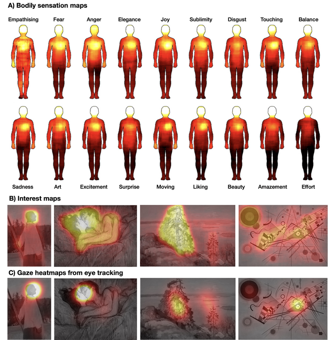
A new study reveals how viewing visual art affects our emotions. The research subjects viewed different kinds of artworks and described the feelings that the art stimulated in their bodies. The researchers recorded the subjects’ eye movement while they viewed the art. In addition, the subjects assessed what kind of emotions each piece of art evoked.

I find the image illustrating the research quite fascinating,

Caption: The image shows the bodily sensations evoked by art (A) as well as the most interesting areas in the paintings (B) and eye movements while viewing the art (C). Credit: Lauri Nummenmaa

A March 27, 2023 University of Turku (Finland) press release (also on EurekAlert), which originated the news item, explains the research,

“Viewing the art evoked many different kinds of feelings and emotions in people. Even though many of the pieces handled sad or scary topics, the emotions that the people experienced were mainly positive. The bodily sensations evoked by art also contributed to the emotions: the stronger the body’s reaction was to the artwork, the stronger were the emotions experienced by the subject,” says Professor Lauri Nummenmaa from the Turku PET Centre at the University of Turku, Finland.

“In the artworks, human figures were the most interesting subject and were looked at the most. People have a tendency to empathise with each other’s emotions and this is probably also the case when we view human figures in art. The human emotions presented in art pieces can be absorbed by the viewer unnoticed, through so-called mirroring,” says Academician Riitta Hari from Aalto University.

Altogether 1,186 people from different countries participated in the study and they assessed the emotions evoked by over 300 artworks. The research was conducted with online surveys and eye movement recordings in the laboratory.

“Our results suggest that our bodies have a significant role in the aesthetic experience. Bodily sensations can draw people to art: art evokes feelings in the body, and such stimulation of the body’s pleasure centres feels pleasant to the viewer. This is why the emotions and bodily sensations evoked by art can be used, for example, in mental health rehabilitation and care,” Professor Nummenmaa recounts. 

Here’s a link to and a citation for the paper,

Bodily feelings and aesthetic experience of art by Lauri Nummenmaa & Riitta Hari. Cognition and Emotion DOI: https://doi.org/10.1080/02699931.2023.2183180 Published online: 13 Mar 2023

This paper is open access.

It looks to me, based on what’s described in the introduction, WikiArt’s homepage (source of the digitized paintings used in the study) and the list of famous paintings, that they have focused heavily on European art, Note 1: Links have been removed; Note 2: Researchers have limited funds and may have to constrain their interests,

Emotion is central to art. Humans all around the world are drawn to creating and consuming art due to its capability to evoke emotions (Chatterjee & Vartanian, Citation2014; Zentner et al., Citation2008), and human emotions are also a central subject of numerous artworks ranging from The Scream by Edvard Munch to The Kiss by Gustav Klimt. Emotions coordinate physiological and behavioural activation patterns to promote survival and govern decision-making across contexts ranging from mate selection (Johnston, Citation2006) to feeding (Spence et al., Citation2016) and environmental preferences (Kaplan, Citation1987). …

Yet, humans may experience powerful emotions in the absence of survival challenges, notably when encountering art. …

The stimuli were digital photographs of 336 paintings and drawings spanning multiple genres and periods. Most of the stimuli were retrieved from the WikiArt Emotions database (Se ID:s in Supplementary Text 1) and were chosen based on their capacity to evoke emotions in the viewers (Mohammad & Kiritchenko, Citation2018). These artworks were complemented with 20 internationally famous paintings and 20 famous Finnish paintings presumably not widely known outside Finland (see Supplementary text 2); this was done to make sure the stimulus contained also well-known and well-liked as well as unfamiliar artworks. …

Suuplementary text 2 [sic?]
Famous Finnish and international paintings included in the study

Finnish: Gunnar Berndtson: Morsiamen laulu, Albert Edelfelt: Lapsen ruumissaatto, Albert Edelfelt: Leikkiviä poikia rannalla, Akseli Gallen-Kallela : Lemminkäisen äiti, Akseli Gallen-Kallela : Symposion, Pekka Halonen: Tienraivaajia Karjalassa, Werner Holmberg: Postitie Hämeessä,Edvard Isto: Hyökkäys, Tove Jansson: Juhlat kaupungissa, Eero Järnfetl: Kaski, Eero Järnfetl: Maisema Kolilta, Juho Rissanen: Kuppari, Juho Rissanen: Lapsuuden muisto, Juho Rissanen: Piipunsytyttäjät, Tyko Sallinen: Piruntanssi, Tyko Sallinen: Saunassa, Helene Schjerfbeck: Toipilas, Hugo Simberg: Haavoittunut Enkeli, Hugo Simberg: Vanhus ja lapsi, Ellen Thesleff: Kaiku. International: Hieronymus Bosch: The Garden of Earthly Delights, Sandro Botticelli: La Primavera, William-Adolphe Bouguereau: The Wave, Francisco de Goya: El Tres de Mayo, Grant Wood: American Gothic, Francisco de Goya: La maja desnuda, Hokusai: The Great Wave off Kanagawa, Edward Hopper: Nighthawks, Wassily Kandinsky: Composition 8, Gustav Klimt: Der Kuss, Édouard Manet: Olympia, Edvard Munch : Aske, Pablo Picasso: The Old Guitarist, Rembrandt van Rijn: Christ in the Storm on the Lake of Galilee, Auguste Renoir: Le Moulin de la Galette, Diego Riviera: The Flower Carrier, Henri Rousseau: The Sleeping Gypsy, Peter Paul Rubens: Massacre of the Innocents, Vincent van Gogh: Starry night, Johannes Vermeer: Meisje met de parel

It would be interesting to find out if there are differences attributable to a viewer’s unconscious assumptions about art, specifically paintings. Would we experience our emotions differently in front of prehistoric art, or ancient Egyptian art, or art uninfluenced by European art?

As it turns out, I have an August 23, 2016 posting titled, “Georgina Lohan, Bharti Kher, and Pablo Picasso: the beauty and the beastliness of art (in Vancouver).”

A new recipe for lignin nanoparticles

A flexible film that does not absorb a drop of water. Photo: Aalto University / Sahar Babaeipour

A November 8, 2022 news item on phys.org announces a new material made of nanocellulose (Note: Links have been removed),

The Bioproduct Chemistry team at Aalto University [Finland] have designed a sustainable method to produce strong and flexible cellulosic films that incredibly maintain their strength even when wet.

The material is made through an innovative combination of wood-based and biodegradable polymers without any chemical modification, harnessing the maximum benefit of each component. For the co-authors in this study, sustainability is a significant motivator in understanding the chemistry of how these materials could work together and developing materials of tomorrow with the functionality we expect today.

A November 7, 2022 Aalto University press release, which originated the news item, explains the interest in cellulose and provides more detail about the research,

Cellulosic materials, which come from the cell walls of plants, have emerged as attractive, sustainable replacements for traditional plastics. However, the moisture sensitivity of cellulose and its incompatibility with many soft hydrophobic polymers are challenges to their widespread application.

From a materials design perspective, gaining the benefit of both hydrophilic cellulose and hydrophobic polymers at the same time without any chemical treatment of raw materials is mystifying. But what if we could engineer their interface with a third component, having favorable interactions with both cellulose and soft polymers such as polycaprolactone (PCL)? To achieve this goal, the team demonstrated that lignin nanoparticles with their well-defined morphology and active surface sites can interact with both cellulose, in this case cellulose nanofibrils, and PCL and act as a compatibilizer between hydrophilic cellulose and hydrophobic PCL. Although it looks complex, the solution is simple.

First, PCL dissolved in an organic solvent is mixed with the lignin nanoparticles in water. The lignin particles assembles at the oil water interface and stabilize the emulsion. Emulsions stabilizes with solid particles are called Pickering emulsions. This emulsion is then mixed with aqueous CNF suspension prior to film formation.  This Pickering emulsion strategy creates an even dispersion of a polymer within the cellulose network, increasing the wet strength and water resistance of the composite, meanwhile retaining all the positive characteristics of the cellulose fibers or fibrils. The outcomes are excellent:  the developed composite has a higher strength than pure CNF nanopaper or pure polymer in both dry and wet conditions, even after fully immersing it in water for a day. ‘When the film was taken out of the water, it looked exactly the same as when it was put into the water,’ says Kimiaei. The reason for this is that the hydrophobic polymer, with the aid of the lignin nanoparticles is now covering the cellulose surface protecting it from the water.

The composite revealed wet strength up to 87 MPa, the highest obtained wet strength for cellulosic composites developed without any direct covalent surface modifications or synthetic additives. Furthermore, this strategy added additional functionality, such as UV shielding and antioxidant properties to the developed composites, making them interesting for packaging applications.

The team at Aalto University in Finland, a country that arguably has the world’s leading experts in the forestry industry, is focused on making the most of these natural and industrial resources. ‘Building the future with forests requires a commitment to sustainable forest management and creating additional value beyond the typical biorefinery and pulp and paper industry,’ says co-author Erfan Kimiaei, a doctoral candidate at Aalto University, School of Chemical Engineering. ‘Understanding the interfacial chemistry of wood components can be the key to getting the most out of this valuable resource in building the sustainable future,’ professor Monika Österberg adds.

For experts in the field, this approach opens new possibilities to eliminate the need for cellulose chemical modification to impart new functionalities, promoting the sustainable use of natural resources from the forest. Furthermore, this research offers a generic foundation for combining hydrophilic cellulose with varied hydrophobic soft polymers to design multifunctional cellulose-based composites using only biodegradable polymers and lignocellulosic materials, taking a big step toward fully sustainable use of natural resources. As a follow up, the researchers are now exploring a broad framework to identify the sustainability of this early-stage technology in environmental and economic aspects by integrating techno-economic and life cycle assessments.

Here’s a link to and a citation for the paper,

Lignin Nanoparticles as an Interfacial Modulator in Tough and Multi-Resistant Cellulose–Polycaprolactone Nanocomposites Based on a Pickering Emulsions Strategy by Erfan Kimiaei, Muhammad Farooq, Rafael Grande, Kristoffer Meinander, Monika Österberg. Advanced Materials Interfaces Volume 9, Issue 27 September 22, 2022 2200988 DOI: https://doi.org/10.1002/admi.202200988 First published online: 25 August 2022

This paper is open access.

Synthesizing a superfluorinated gold nanocluster with a core of 25 gold atoms,

A June 21, 2022 Politecnico di Milano press release (also on EurekAlert but published June 15, 2022) describes work that researchers believe could be instrumental in precision medicine and the production of ‘green’ hydrogen,

The SupraBioNano Lab (SBNLab) at the Politecnico di Milano’s Department of Chemistry, Materials and Chemical Engineering “Giulio Natta”, in partnership with the University of Bologna and the Aalto University of Helsinki (Finland) has, for the first time, synthesised a superfluorinated gold nanocluster, made up of a core of only 25 gold atoms, to which 18 branch-structured fluorinated molecules are linked.

The metal clusters are an innovative class of very complex nanomaterial, characterised by ultra-small dimensions (<2nm) and peculiar chemical-physical properties such as luminescence and catalytic activity, which encourage its application in various scientific fields of high importance in relation to modern global challenges. These include precision medicine, in which metal nanoclusters are used as innovative probes for diagnostic and therapeutic applications, and the energy transition, where they are applied as efficient catalysers for the production of green hydrogen.

The crystallisation of metal nanoclusters offers the possibility of obtaining high-purity samples, allowing their fine atomic structure to be determined; however, at present this remains a very difficult process to control. The methodologies developed in this study promoted the crystallisation of nanoclusters, allowing their atomic structure to be determined. The end result is the structural description of the most complex fluorinated nano-object ever reported.

The atomic structure has been determined by means of x-ray diffraction at the Sincrotrone Elettra in Trieste. It will soon be possible to study the structure of these advanced nanomaterials at the Politecnico di Milano, where – thanks also to the grant from the Region of Lombardy – Next-GAME (Next-Generation Advanced Materials), a laboratory dedicated to the use of state-of-the-art x-ray instruments to characterise crystals, nanoparticles and colloids, is being established.

Among the authors of the study were Prof. Pierangelo Metrangolo, Prof. Giancarlo Terraneo, Prof. Valentina Dichiarante, Prof. Francesca Baldelli Bombelli, Dr. Claudia Pigliacelli (SBNLab); professor Giulio Cerullo, from the Politecnico di Milano’s Department of Physics, also contributed to the study, looking at the nanocluster’s optical characteristics and demonstrating the fluorinated binders’ impact on the gold core’s optical activity.

Here’s a link to and a citation for the paper,

High-resolution crystal structure of a 20 kDa superfluorinated gold nanocluster by Claudia Pigliacelli, Angela Acocella, Isabel Díez, Luca Moretti, Valentina Dichiarante, Nicola Demitri, Hua Jiang, Margherita Maiuri, Robin H. A. Ras, Francesca Baldelli Bombelli, Giulio Cerullo, Francesco Zerbetto, Pierangelo Metrangolo & Giancarlo Terraneo. Nature Communications volume 13, Article number: 2607 (2022) DOI https://doi.org/10.1038/s41467-022-29966-2 Published11 May 2022 DOI https://doi.org/10.1038/s41467-022-29966-2

This paper is open access.

Radiation-free quantum technology with graphene

A July 8, 2021 news item on Nanowerk announces research from Finland and Switzerland that could have an impact on real world quantum technologies (Note: A link has been removed),

Rare-earth compounds have fascinated researchers for decades due to the unique quantum properties they display, which have so far remained totally out of reach of everyday compounds. One of the most remarkable and exotic properties of those materials is the emergence of exotic superconducting states, and particularly the superconducting states required to build future topological quantum computers.

While these specific rare-earth compounds, known as heavy fermion superconductors, have been known for decades, making usable quantum technologies out of them has remained a critically open challenge. This is because these materials contain critically radioactive compounds, such as uranium and plutonium, rendering them of limited use in real-world quantum technologies.

New research has now revealed an alternative pathway to engineer the fundamental phenomena of these rare-earth compounds solely with graphene, which has none of the safety problems of traditional rare-earth compounds.

The exciting result in the new paper shows how a quantum state known as a “heavy fermion” can be produced by combining three twisted graphene layers. A heavy fermion is a particle – in this case an electron – that behaves like it has a lot more mass than it actually does. The reason it behaves this way stems from unique quantum many-body effects that were mostly only observed in rare-earth compounds until now.

This heavy fermion behavior is known to be the driving force of the phenomena required to use these materials for topological quantum computing. This new result demonstrates a new, non-radioactive way of achieving this effect using only carbon, opening up a pathway for sustainably exploiting heavy fermion physics in quantum technologies.

A July 8, 2021 Aalto University press release (also on EurekAlert), which originated the news item, provides more details,

In the paper authored by Aline Ramires, (Paul Scherrer Institute, Switzerland) and Jose Lado (Aalto University), the researchers show how it is possible to create heavy fermions with cheap, non-radioactive materials. To do this, they used graphene, which is a one-atom thick layer of carbon. Despite being chemically identical to the material that is used in regular pencils, the sub-nanometre thickness of graphene means that it has unexpectedly unique electrical properties. By layering the thin sheets of carbon on top of one another in a specific pattern, where each sheet is rotated in relation to the other, the researchers can create the quantum properties effect that results in the electrons in the graphene behaving like heavy fermions.

“Until now, practical applications of heavy fermion superconductors for topological quantum computing has not been pursued much, partially because it required compounds containing uranium and plutonium, far from ideal for applications due to their radioactive nature”, says Professor Lado, “In this work we show that one can aim to realize the exactly very same physics just with graphene. While in this work we only show the emergence of heavy fermion behavior, addressing the emergence of topological superconductivity is a natural next step, which could potentially have a groundbreaking impact for topological quantum computing.”

Topological superconductivity is a topic of critical interest for quantum technologies, also tackled by alternative strategies in other papers from Aalto University Department of Applied Physics, including a previous paper by Professor Lado. “These results potentially provide a carbon-based platform for exploitation of heavy fermion phenomena in quantum technologies, without requiring rare-earth elements”, concludes Professor Lado.

Here’s a link to and a citation for the paper,

Emulating Heavy Fermions in Twisted Trilayer Graphene by Aline Ramires and Jose L. Lado. Phys. Rev. Lett. 127, 026401 DOI: https://doi.org/10.1103/PhysRevLett.127.026401 Published 7 July 2021 © 2021 American Physical Society

This paper is behind a paywall.

Graphene and its magnetism

I have two news bits about graphene and magnetism. If I understood what I was reading, one is more focused on applications and the other is focused on further establishing the field of valleytronics.

University of Cambridge and superconductivity

A February 8, 2021 news item on Nanowerk announces ‘magnetic work’ from the University of Cambridge (Note: A link has been removed),

The researchers, led by the University of Cambridge, were able to control the conductivity and magnetism of iron thiophosphate (FePS3), a two-dimensional material which undergoes a transition from an insulator to a metal when compressed. This class of magnetic materials offers new routes to understanding the physics of new magnetic states and superconductivity.

Using new high-pressure techniques, the researchers have shown what happens to magnetic graphene during the transition from insulator to conductor and into its unconventional metallic state, realised only under ultra-high pressure conditions. When the material becomes metallic, it remains magnetic, which is contrary to previous results and provides clues as to how the electrical conduction in the metallic phase works. The newly discovered high-pressure magnetic phase likely forms a precursor to superconductivity so understanding its mechanisms is vital.

Their results, published in the journal Physical Review X, also suggest a way that new materials could be engineered to have combined conduction and magnetic properties, which could be useful in the development of new technologies such as spintronics, which could transform the way in which computers process information.

A February 8, 2021 University of Cambridge press release (also on EurekAlert), which originated the news item, delves into the topic,

Properties of matter can alter dramatically with changing dimensionality. For example, graphene, carbon nanotubes, graphite and diamond are all made of carbon atoms, but have very different properties due to their different structure and dimensionality.

“But imagine if you were also able to change all of these properties by adding magnetism,” said first author Dr Matthew Coak, who is jointly based at Cambridge’s Cavendish Laboratory and the University of Warwick. “A material which could be mechanically flexible and form a new kind of circuit to store information and perform computation. This is why these materials are so interesting, and because they drastically change their properties when put under pressure so we can control their behaviour.”

In a previous study by Sebastian Haines of Cambridge’s Cavendish Laboratory and the Department of Earth Sciences, researchers established that the material becomes a metal at high pressure, and outlined how the crystal structure and arrangement of atoms in the layers of this 2D material change through the transition.

“The missing piece has remained however, the magnetism,” said Coak. “With no experimental techniques able to probe the signatures of magnetism in this material at pressures this high, our international team had to develop and test our own new techniques to make it possible.”

The researchers used new techniques to measure the magnetic structure up to record-breaking high pressures, using specially designed diamond anvils and neutrons to act as the probe of magnetism. They were then able to follow the evolution of the magnetism into the metallic state.

“To our surprise, we found that the magnetism survives and is in some ways strengthened,” co-author Dr Siddharth Saxena, group leader at the Cavendish Laboratory. “This is unexpected, as the newly-freely-roaming electrons in a newly conducting material can no longer be locked to their parent iron atoms, generating magnetic moments there – unless the conduction is coming from an unexpected source.”

In their previous paper, the researchers showed these electrons were ‘frozen’ in a sense. But when they made them flow or move, they started interacting more and more. The magnetism survives, but gets modified into new forms, giving rise to new quantum properties in a new type of magnetic metal.

How a material behaves, whether conductor or insulator, is mostly based on how the electrons, or charge, move around. However, the ‘spin’ of the electrons has been shown to be the source of magnetism. Spin makes electrons behave a bit like tiny bar magnets and point a certain way. Magnetism from the arrangement of electron spins is used in most memory devices: harnessing and controlling it is important for developing new technologies such as spintronics, which could transform the way in which computers process information.

“The combination of the two, the charge and the spin, is key to how this material behaves,” said co-author Dr David Jarvis from the Institut Laue-Langevin, France, who carried out this work as the basis of his PhD studies at the Cavendish Laboratory. “Finding this sort of quantum multi-functionality is another leap forward in the study of these materials.”

“We don’t know exactly what’s happening at the quantum level, but at the same time, we can manipulate it,” said Saxena. “It’s like those famous ‘unknown unknowns’: we’ve opened up a new door to properties of quantum information, but we don’t yet know what those properties might be.”

There are more potential chemical compounds to synthesise than could ever be fully explored and characterised. But by carefully selecting and tuning materials with special properties, it is possible to show the way towards the creation of compounds and systems, but without having to apply huge amounts of pressure.

Additionally, gaining fundamental understanding of phenomena such as low-dimensional magnetism and superconductivity allows researchers to make the next leaps in materials science and engineering, with particular potential in energy efficiency, generation and storage.

As for the case of magnetic graphene, the researchers next plan to continue the search for superconductivity within this unique material. “Now that we have some idea what happens to this material at high pressure, we can make some predictions about what might happen if we try to tune its properties through adding free electrons by compressing it further,” said Coak.

“The thing we’re chasing is superconductivity,” said Saxena. “If we can find a type of superconductivity that’s related to magnetism in a two-dimensional material, it could give us a shot at solving a problem that’s gone back decades.”

The citation and link to the paper are at the end of this blog posting.

Aalto University’s valleytronics

Further north in Finland, researchers at Aalto University make some advances applicable to the field of valleytronics, from a February 5, 2021 Aalto University press release (also on EurekAltert but published February 8, 2021),

Electrons in materials have a property known as ‘spin’, which is responsible for a variety of properties, the most well-known of which is magnetism. Permanent magnets, like the ones used for refrigerator doors, have all the spins in their electrons aligned in the same direction. Scientists refer to this behaviour as ferromagnetism, and the research field of trying to manipulate spin as spintronics.

Down in the quantum world, spins can arrange in more exotic ways, giving rise to frustrated states and entangled magnets. Interestingly, a property similar to spin, known as “the valley,” appears in graphene materials. This unique feature has given rise to the field of valleytronics, which aims to exploit the valley property for emergent physics and information processing, very much like spintronics relies on pure spin physics.

‘Valleytronics would potentially allow encoding information in the quantum valley degree of freedom, similar to how electronics do it with charge and spintronics with the spin.’ Explains Professor Jose Lado, from Aalto’s Department of applied physics, and one of the authors of the work. ‘What’s more, valleytronic devices would offer a dramatic increase in the processing speeds in comparison with electronics, and with much higher stability towards magnetic field noise in comparison with spintronic devices.’

Structures made of rotated, ultra-thin materials provide a rich solid-state platform for designing novel devices. In particular, slightly twisted graphene layers have recently been shown to have exciting unconventional properties, that can ultimately lead to a new family of materials for quantum technologies. These unconventional states which are already being explored depend on electrical charge or spin. The open question is if the valley can also lead to its own family of exciting states.

Making materials for valleytronics

For this goal, it turns out that conventional ferromagnets play a vital role, pushing graphene to the realms of valley physics. In a recent work, Ph.D. student Tobias Wolf, together with Profs. Oded Zilberberg and Gianni Blatter at ETH Zurich, and Prof. Jose Lado at Aalto University, showed a new direction for correlated physics in magnetic van der Waals materials.

The team showed that sandwiching two slightly rotated layers of graphene between a ferromagnetic insulator provides a unique setting for new electronic states. The combination of ferromagnets, graphene’s twist engineering, and relativistic effects force the “valley” property to dominate the electrons behaviour in the material. In particular, the researchers showed how these valley-only states can be tuned electrically, providing a materials platform in which valley-only states can be generated. Building on top of the recent breakthrough in spintronics and van der Waals materials, valley physics in magnetic twisted van der Waals multilayers opens the door to the new realm of correlated twisted valleytronics.

‘Demonstrating these states represents the starting point towards new exotic entangled valley states.’ Said Professor Lado, ‘Ultimately, engineering these valley states can allow realizing quantum entangled valley liquids and fractional quantum valley Hall states. These two exotic states of matter have not been found in nature yet, and would open exciting possibilities towards a potentially new graphene-based platform for topological quantum computing.’

Citations and links

Here’s a link to and a citation for the University of Cambridge research,

Emergent Magnetic Phases in Pressure-Tuned van der Waals Antiferromagnet FePS3 by Matthew J. Coak, David M. Jarvis, Hayrullo Hamidov, Andrew R. Wildes, Joseph A. M. Paddison, Cheng Liu, Charles R. S. Haines, Ngoc T. Dang, Sergey E. Kichanov, Boris N. Savenko, Sungmin Lee, Marie Kratochvílová, Stefan Klotz, Thomas C. Hansen, Denis P. Kozlenko, Je-Geun Park, and Siddharth S. Saxena. Phys. Rev. X 11, 011024 DOI: https://doi.org/10.1103/PhysRevX.11.011024 Published 5 February 2021

This article appears to be open access.

Here’s a link to and a citation for the Aalto University research,

Spontaneous Valley Spirals in Magnetically Encapsulated Twisted Bilayer Graphene by Tobias M. R. Wolf, Oded Zilberberg, Gianni Blatter, and Jose L. Lado. Phys. Rev. Lett. 126, 056803 DOI: https://doi.org/10.1103/PhysRevLett.126.056803 Published 4 February 2021

This paper is behind a paywall.

Carbon nanotubes (CNTs) in 466 colours

Caption: A color map illustrates the inherent colors of 466 types of carbon nanotubes with unique (n,m) designations based their chiral angle and diameter. Credit: Image courtesy of Kauppinen Group/Aalto University

This is, so to speak, a new angle on carbon nanotubes (CNTs). It’s also the first time I’ve seen two universities place identical news releases on EurekAlert under their individual names.

From the Dec. 14, 2020 Rice University (US) news release or the Dec. 14, 2020 Aalto University (Finland) press release on EurekAlert,

Nanomaterials researchers in Finland, the United States and China have created a color atlas for 466 unique varieties of single-walled carbon nanotubes.

The nanotube color atlas is detailed in a study in Advanced Materials about a new method to predict the specific colors of thin films made by combining any of the 466 varieties. The research was conducted by researchers from Aalto University in Finland, Rice University and Peking University in China.

“Carbon, which we see as black, can appear transparent or take on any color of the rainbow,” said Aalto physicist Esko Kauppinen, the corresponding author of the study. “The sheet appears black if light is completely absorbed by carbon nanotubes in the sheet. If less than about half of the light is absorbed in the nanotubes, the sheet looks transparent. When the atomic structure of the nanotubes causes only certain colors of light, or wavelengths, to be absorbed, the wavelengths that are not absorbed are reflected as visible colors.”

Carbon nanotubes are long, hollow carbon molecules, similar in shape to a garden hose but with sides just one atom thick and diameters about 50,000 times smaller than a human hair. The outer walls of nanotubes are made of rolled graphene. And the wrapping angle of the graphene can vary, much like the angle of a roll of holiday gift wrap paper. If the gift wrap is rolled carefully, at zero angle, the ends of the paper will align with each side of the gift wrap tube. If the paper is wound carelessly, at an angle, the paper will overhang on one end of the tube.

The atomic structure and electronic behavior of each carbon nanotube is dictated by its wrapping angle, or chirality, and its diameter. The two traits are represented in a “(n,m)” numbering system that catalogs 466 varieties of nanotubes, each with a characteristic combination of chirality and diameter. Each (n,m) type of nanotube has a characteristic color.

Kauppinen’s research group has studied carbon nanotubes and nanotube thin films for years, and it previously succeeded in mastering the fabrication of colored nanotube thin films that appeared green, brown and silver-grey.

In the new study, Kauppinen’s team examined the relationship between the spectrum of absorbed light and the visual color of various thicknesses of dry nanotube films and developed a quantitative model that can unambiguously identify the coloration mechanism for nanotube films and predict the specific colors of films that combine tubes with different inherent colors and (n,m) designations.

Rice engineer and physicist Junichiro Kono, whose lab solved the mystery of colorful armchair nanotubes in 2012, provided films made solely of (6,5) nanotubes that were used to calibrate and verify the Aalto model. Researchers from Aalto and Peking universities used the model to calculate the absorption of the Rice film and its visual color. Experiments showed that the measured color of the film corresponded quite closely to the color forecast by the model.

The Aalto model shows that the thickness of a nanotube film, as well as the color of nanotubes it contains, affects the film’s absorption of light. Aalto’s atlas of 466 colors of nanotube films comes from combining different tubes. The research showed that the thinnest and most colorful tubes affect visible light more than those with larger diameters and faded colors.

“Esko’s group did an excellent job in theoretically explaining the colors, quantitatively, which really differentiates this work from previous studies on nanotube fluorescence and coloration,” Kono said.

Since 2013, Kono’s lab has pioneered a method for making highly ordered 2D nanotube films. Kono said he had hoped to supply Kauppinen’s team with highly ordered 2D crystalline films of nanotubes of a single chirality.

“That was the original idea, but unfortunately, we did not have appropriate single-chirality aligned films at that time,” Kono said. “In the future, our collaboration plans to extend this work to study polarization-dependent colors in highly ordered 2D crystalline films.”

The experimental method the Aalto researchers used to grow nanotubes for their films was the same as in their previous studies: Nanotubes grow from carbon monoxide gas and iron catalysts in a reactor that is heated to more than 850 degrees Celsius. The growth of nanotubes with different colors and (n,m) designations is regulated with the help of carbon dioxide that is added to the reactor.

“Since the previous study, we have pondered how we might explain the emergence of the colors of the nanotubes,” said Nan Wei, an assistant research professor at Peking University who previously worked as a postdoctoral researcher at Aalto. “Of the allotropes of carbon, graphite and charcoal are black, and pure diamonds are colorless to the human eye. However, now we noticed that single-walled carbon nanotubes can take on any color: for example, red, blue, green or brown.”

Kauppinen said colored thin films of nanotubes are pliable and ductile and could be useful in colored electronics structures and in solar cells.

“The color of a screen could be modified with the help of a tactile sensor in mobile phones, other touch screens or on top of window glass, for example,” he said.

Kauppinen said the research can also provide a foundation for new kinds of environmentally friendly dyes.

Here’s a link to and a citation for the paper,

Colors of Single‐Wall Carbon Nanotubes by Nan Wei, Ying Tian, Yongping Liao, Natsumi Komatsu, Weilu Gao, Alina Lyuleeva‐Husemann, Qiang Zhang, Aqeel Hussain, Er‐Xiong Ding, Fengrui Yao, Janne Halme. Kaihui Liu, Junichiro Kono, Hua Jiang, Esko I. Kauppinen. Advanced Materials DOI: https://doi.org/10.1002/adma.202006395 First published: 14 December 2020

Thi8s paper is open access.

New capacitor for better wearable electronics?

Supercapacitors are a predictable source of scientific interest and excitement. The latest entry in the ‘supercapacitor stakes’ is from a Russian/Finnish/US team according to a June 11, 2020 Skoltech (Skolkovo Institute of Science and Technology) press release (also on EurekAlert),

Researchers from Skoltech [Russia], Aalto University [Finland] and Massachusetts Institute of Technology [MIT; US] have designed a high-performance, low-cost, environmentally friendly, and stretchable supercapacitor that can potentially be used in wearable electronics. The paper was published in the Journal of Energy Storage.

Supercapacitors, with their high power density, fast charge-discharge rates, long cycle life, and cost-effectiveness, are a promising power source for everything from mobile and wearable electronics to electric vehicles. However, combining high energy density, safety, and eco-friendliness in one supercapacitor suitable for small devices has been rather challenging.

“Usually, organic solvents are used to increase the energy density. These are hazardous, not environmentally friendly, and they reduce the power density compared to aqueous electrolytes with higher conductivity,” says Professor Tanja Kallio from Aalto University, a co-author of the paper.

The researchers proposed a new design for a “green” and simple-to-fabricate supercapacitor. It consists of a solid-state material based on nitrogen-doped graphene flake electrodes distributed in the NaCl-containing hydrogel electrolyte. This structure is sandwiched between two single-walled carbon nanotube film current collectors, which provides stretchability. Hydrogel in the supercapacitor design enables compact packing and high energy density and allows them to use the environmentally friendly electrolyte.

The scientists managed to improve the volumetric capacitive performance, high energy density and power density for the prototype over analogous supercapacitors described in previous research. “We fabricated a prototype with unchanged performance under the 50% strain after a thousand stretching cycles. To ensure lower cost and better environmental performance, we used a NaCl-based electrolyte. Still the fabrication cost can be lowered down by implementation of 3D printing or other advanced fabrication techniques,” concluded Skoltech professor Albert Nasibulin.

Here’s a link to and a citation for the paper,

Superior environmentally friendly stretchable supercapacitor based on nitrogen-doped graphene/hydrogel and single-walled carbon nanotubes by Evgeniia Gilshtein, Cristina Flox, Farhan S.M. Ali, Bahareh Mehrabimatin, Fedor S.Fedorov, Shaoting Lin, Xuanhe Zhao, Albert G. Nasibulin, Tanja Kallio. Journal of Energy Storage Volume 30, August 2020, 101505 DOI: https://doi.org/10.1016/j.est.2020.101505

This paper is behind a paywall.

I’m trying to remember if I’ve ever before seen a material that combines graphene and single-walled carbon nanotubes (SWCNTs). Anyway, here’s an image the researchers are using illustrate their work,

Caption: This is an outline of the new supercapacitor. Credit: Pavel Odinev / Skoltech

Colo(u)ring your carbon nanotubes

Finnish research is highlighted in an August 28, 2018 news item on phys.org,

A method developed at Aalto University, Finland, can produce large quantities of pristine single-walled carbon nanotubes in select shades of the rainbow. The secret is a fine-tuned fabrication process—and a small dose of carbon dioxide. The films could find applications in touch screen technologies or as coating agents for new types of solar cells.

An August 28, 2018 Aalto University press release (also on EurekAlert), which originated the news item, provides more detail,

Samples of the colourful carbon nanotube thin films, as produced in the fabrication reactor. Image: Aalto University.
 

Single-walled carbon nanotubes, or sheets of one atom-thick layers of graphene rolled up into different sizes and shapes, have found many uses in electronics and new touch screen devices. By nature, carbon nanotubes are typically black or a dark grey.

In their new study published in the Journal of the American Chemical Society (JACS), Aalto University researchers present a way to control the fabrication of carbon nanotube thin films so that they display a variety of different colours—for instance, green, brown, or a silvery grey.

The researchers believe this is the first time that coloured carbon nanotubes have been produced by direct synthesis. Using their invention, the colour is induced straight away in the fabrication process, not by employing a range of purifying techniques on finished, synthesized tubes.

With direct synthesis, large quantities of clean sample materials can be produced while also avoiding damage to the product in the purifying process—which makes it the most attractive approach for applications.

‘In theory, these coloured thin films could be used to make touch screens with many different colours, or solar cells that display completely new types of optical properties,’ says Esko Kauppinen, Professor at Aalto University.

To get carbon structures to display colours is a feat in itself. The underlying techniques needed to enable the colouration also imply finely detailed control of the structure of the nanotube structures. Kauppinen and his team’s unique method, which uses aerosols of metal and carbon, allows them to carefully manipulate and control the nanotube structure directly from the fabrication process.

‘Growing carbon nanotubes is, in a way, like planting trees: we need seeds, feeds, and solar heat. For us, aerosol nanoparticles of iron work as a catalyst or seed, carbon monoxide as the source for carbon, so feed, and a reactor gives heat at a temperature more than 850 degrees Celsius,’ says Dr. Hua Jiang, Senior Scientist at Aalto University.

Professor Kauppinen’s group has a long history of using these very resources in their singular production method. To add to their repertoire, they have recently experimented with administering small doses of carbon dioxide into the fabrication process.

‘Carbon dioxide acts as a kind of graft material that we can use to tune the growth of carbon nanotubes of various colors,’ explains Jiang.

With an advanced electron diffraction technique, the researchers were able to find out the precise atomic scale structure of their thin films. They found that they have very narrow chirality distributions, meaning that the orientation of the honeycomb-lattice of the tubes’ walls is almost uniform throughout the sample. The chirality more or less dictates the electrical properties carbon nanotubes can have, as well as their colour.

The method developed at Aalto University promises a simple and highly scalable way to fabricate carbon nanotube thin films in high yields.

‘Usually you have to choose between mass production or having good control over the structure of carbon nanotubes. With our breakthrough, we can do both,’ trusts Dr. Qiang Zhang, a postdoctoral researcher in the group.

Follow-up work is already underway.

‘We want to understand the science of how the addition of carbon dioxide tunes the structure of the nanotubes and creates colours. Our aim is to achieve full control of the growing process so that single-walled carbon nanotubes could be used as building blocks for the next generation of nanoelectronics devices,’ says professor Kauppinen.

Here’s a link to and a citation for the paper,

Direct Synthesis of Colorful Single-Walled Carbon Nanotube Thin Films by Yongping Liao, Hua Jiang, Nan Wei, Patrik Laiho, Qiang Zhang, Sabbir A. Khan, and Esko I. Kauppinen. J. Am. Chem. Soc., 2018, 140 (31), pp 9797–9800 DOI: 10.1021/jacs.8b05151 Publication Date (Web): July 26, 2018

Copyright © 2018 American Chemical Society

This paper appears to be open access.

For the curious, here’s a peek at the coloured carbon nanotube films,


Caption: Samples of the colorful carbon nanotube thin films, as produced in the fabrication reactor. Credit: Authors / Aalto University

Quantum entanglement in near-macroscopic objects

Researchers at Finland’s Aalto University seem excited in an April 25, 2018 news item on phys.org,

Perhaps the strangest prediction of quantum theory is entanglement, a phenomenon whereby two distant objects become intertwined in a manner that defies both classical physics and a common-sense understanding of reality. In 1935, Albert Einstein expressed his concern over this concept, referring to it as “spooky action at a distance.”

Today, entanglement is considered a cornerstone of quantum mechanics, and it is the key resource for a host of potentially transformative quantum technologies. Entanglement is, however, extremely fragile, and it has previously been observed only in microscopic systems such as light or atoms, and recently in superconducting electric circuits.

In work recently published in Nature, a team led by Prof. Mika Sillanpää at Aalto University in Finland has shown that entanglement of massive objects can be generated and detected.

The researchers managed to bring the motions of two individual vibrating drumheads—fabricated from metallic aluminium on a silicon chip—into an entangled quantum state. The macroscopic objects in the experiment are truly massive compared to the atomic scale—the circular drumheads have a diametre similar to the width of a thin human hair.

An April 20,2018 Aalto University press release (also on EurekAlert), which originated the news item, provides more detail,

‘The vibrating bodies are made to interact via a superconducting microwave circuit. The electromagnetic fields in the circuit carry away any thermal disturbances, leaving behind only the quantum mechanical vibrations’, says Professor Sillanpää, describing the experimental setup.

Eliminating all forms of external noise is crucial for the experiments, which is why they have to be conducted at extremely low temperatures near absolute zero, at –273 °C. Remarkably, the experimental approach allows the unusual state of entanglement to persist for long periods of time, in this case up to half an hour. In comparison, measurements on elementary particles have witnessed entanglement to last only tiny fractions of a second.

‘These measurements are challenging but extremely fascinating. In the future, we will attempt to teleport the mechanical vibrations. In quantum teleportation, properties of physical bodies can be transmitted across arbitrary distances using the channel of “spooky action at a distance”. We are still pretty far from Star Trek, though,’ says Dr. Caspar Ockeloen-Korppi, the lead author on the work, who also performed the measurements.

The results demonstrate that it is now possible to have control over the most delicate properties of objects whose size approaches the scale of our daily lives. The achievement opens doors for new kinds of quantum technologies, where the entangled drumheads could be used as routers or sensors. The finding also enables new studies of fundamental physics in, for example, the poorly understood interplay of gravity and quantum mechanics.

The team also included scientists from the University of New South Wales in Australia, the University of Chicago in the USA, and the University of Jyväskylä in Finland, whose theoretical innovations paved the way for the laboratory experiment.

An illustration has been made available,

An illustration of the 15-micrometre-wide drumheads prepared on silicon chips used in the experiment. The drumheads vibrate at a high ultrasound frequency, and the peculiar quantum state predicted by Einstein was created from the vibrations. Image: Aalto University / Petja Hyttinen & Olli Hanhirova, ARKH Architects.

Here’s a link to and a citation for the paper,

Stabilized entanglement of massive mechanical oscillators by C. F. Ockeloen-Korppi, E. Damskägg, J.-M. Pirkkalainen, M. Asjad, A. A. Clerk, F. Massel, M. J. Woolley & M. A. Sillanpää. Nature volume 556, pages478–482 (2018) doi:10.1038/s41586-018-0038-x Published online: 25 April 2018

This paper is behind a paywall.

New breed of memristors?

This new ‘breed’ of memristor (a component in brain-like/neuromorphic computing) is a kind of thin film. First, here’s an explanation of neuromorphic computing from the Finnish researchers looking into a new kind of memristor, from a January 10, 2018 news item on Nanowerk,

The internet of things [IOT] is coming, that much we know. But still it won’t; not until we have components and chips that can handle the explosion of data that comes with IoT. In 2020, there will already be 50 billion industrial internet sensors in place all around us. A single autonomous device – a smart watch, a cleaning robot, or a driverless car – can produce gigabytes of data each day, whereas an airbus may have over 10 000 sensors in one wing alone.

Two hurdles need to be overcome. First, current transistors in computer chips must be miniaturized to the size of only few nanometres; the problem is they won’t work anymore then. Second, analysing and storing unprecedented amounts of data will require equally huge amounts of energy. Sayani Majumdar, Academy Fellow at Aalto University, along with her colleagues, is designing technology to tackle both issues.

Majumdar has with her colleagues designed and fabricated the basic building blocks of future components in what are called “neuromorphic” computers inspired by the human brain. It’s a field of research on which the largest ICT companies in the world and also the EU are investing heavily. Still, no one has yet come up with a nano-scale hardware architecture that could be scaled to industrial manufacture and use.

An Aalto University January 10, 2018 press release, which originated the news item, provides more detail about the work,

“The technology and design of neuromorphic computing is advancing more rapidly than its rival revolution, quantum computing. There is already wide speculation both in academia and company R&D about ways to inscribe heavy computing capabilities in the hardware of smart phones, tablets and laptops. The key is to achieve the extreme energy-efficiency of a biological brain and mimic the way neural networks process information through electric impulses,” explains Majumdar.

Basic components for computers that work like the brain

In their recent article in Advanced Functional Materials, Majumdar and her team show how they have fabricated a new breed of “ferroelectric tunnel junctions”, that is, few-nanometre-thick ferroelectric thin films sandwiched between two electrodes. They have abilities beyond existing technologies and bode well for energy-efficient and stable neuromorphic computing.

The junctions work in low voltages of less than five volts and with a variety of electrode materials – including silicon used in chips in most of our electronics. They also can retain data for more than 10 years without power and be manufactured in normal conditions.

Tunnel junctions have up to this point mostly been made of metal oxides and require 700 degree Celsius temperatures and high vacuums to manufacture. Ferroelectric materials also contain lead which makes them – and all our computers – a serious environmental hazard.

“Our junctions are made out of organic hydro-carbon materials and they would reduce the amount of toxic heavy metal waste in electronics. We can also make thousands of junctions a day in room temperature without them suffering from the water or oxygen in the air”, explains Majumdar.

What makes ferroelectric thin film components great for neuromorphic computers is their ability to switch between not only binary states – 0 and 1 – but a large number of intermediate states as well. This allows them to ‘memorise’ information not unlike the brain: to store it for a long time with minute amounts of energy and to retain the information they have once received – even after being switched off and on again.

We are no longer talking of transistors, but ‘memristors’. They are ideal for computation similar to that in biological brains.  Take for example the Mars 2020 Rover about to go chart the composition of another planet. For the Rover to work and process data on its own using only a single solar panel as an energy source, the unsupervised algorithms in it will need to use an artificial brain in the hardware.

“What we are striving for now, is to integrate millions of our tunnel junction memristors into a network on a one square centimetre area. We can expect to pack so many in such a small space because we have now achieved a record-high difference in the current between on and off-states in the junctions and that provides functional stability. The memristors could then perform complex tasks like image and pattern recognition and make decisions autonomously,” says Majumdar.

The probe-station device (the full instrument, left, and a closer view of the device connection, right) which measures the electrical responses of the basic components for computers mimicking the human brain. The tunnel junctions are on a thin film on the substrate plate. Photo: Tapio Reinekoski

Here’s a link to and a citation for the paper,

Electrode Dependence of Tunneling Electroresistance and Switching Stability in Organic Ferroelectric P(VDF-TrFE)-Based Tunnel Junctions by Sayani Majumdar, Binbin Chen, Qi Hang Qin, Himadri S. Majumdar, and Sebastiaan van Dijken. Advanced Functional Materials Vol. 28 Issue 2 DOI: 10.1002/adfm.201703273 Version of Record online: 27 NOV 2017

© 2017 WILEY-VCH Verlag GmbH & Co. KGaA, Weinheim

This paper is behind a paywall.