If ‘chisel’ made you think of sculpting, you are correct. The researchers are alluding to the process of sculpting in their research.
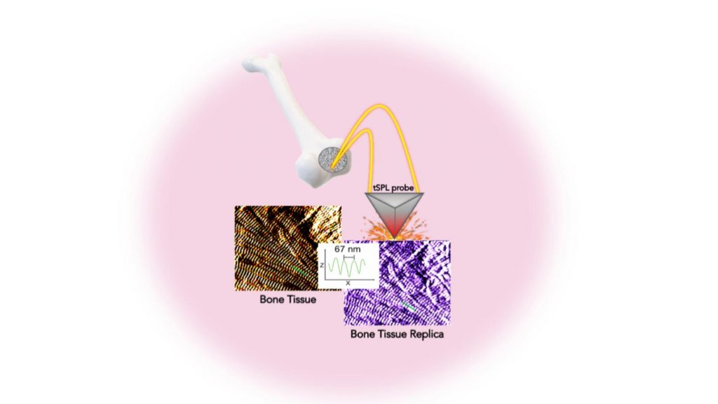
Researchers were able to replicate — with sub-15 nm resolution — bone tissue structure in a biocompatible material using thermal scanning probe lithography. This method opens up unprecedented possibilities for pioneering new stem cell studies and biomedical applications. Courtesy: New York University Tandon School of Engineering
A holy grail for orthopedic research is a method for not only creating artificial bone tissue that precisely matches the real thing, but does so in such microscopic detail that it includes tiny structures potentially important for stem cell differentiation, which is key to bone regeneration.
Researchers at the NYU [New York University] Tandon School of Engineering and New York Stem Cell Foundation Research Institute (NYSF) have taken a major step by creating the exact replica of a bone using a system that pairs biothermal imaging with a heated “nano-chisel.” In a study, “Cost and Time Effective Lithography of Reusable Millimeter Size Bone Tissue Replicas with Sub-15 nm Feature Size on a Biocompatible Polymer,” which appears in the journal Advanced Functional Materials, the investigators detail a system allowing them to sculpt, in a biocompatible material, the exact structure of the bone tissue, with features smaller than the size of a single protein—a billion times smaller than a meter. This platform, called, bio-thermal scanning probe lithography (bio-tSPL), takes a “photograph” of the bone tissue, and then uses the photograph to produce a bona-fide replica of it.
The team, led by Elisa Riedo, professor of chemical and biomolecular engineering at NYU Tandon, and Giuseppe Maria de Peppo, a Ralph Lauren Senior Principal Investigator at the NYSF, demonstrated that it is possible to scale up bio-tSPL to produce bone replicas on a size meaningful for biomedical studies and applications, at an affordable cost. These bone replicas support the growth of bone cells derived from a patient’s own stem cells, creating the possibility of pioneering new stem cell applications with broad research and therapeutic potential. This technology could revolutionize drug discovery and result in the development of better orthopedic implants and devices.
In the human body, cells live in specific environments that control their behavior and support tissue regeneration via provision of morphological and chemical signals at the molecular scale. In particular, bone stem cells are embedded in a matrix of fibers — aggregates of collagen molecules, bone proteins, and minerals. The bone hierarchical structure consists of an assembly of micro- and nano- structures, whose complexity has hindered their replication by standard fabrication methods so far.
“tSPL is a powerful nanofabrication method that my lab pioneered a few years ago, and it is at present implemented by using a commercially available instrument, the NanoFrazor,” said Riedo. “However, until today, limitations in terms of throughput and biocompatibility of the materials have prevented its use in biological research. We are very excited to have broken these barriers and to have led tSPL into the realm of biomedical applications.”
Its time- and cost-effectiveness, as well as the cell compatibility and reusability of the bone replicas, make bio-tSPL an affordable platform for the production of surfaces that perfectly reproduce any biological tissue with unprecedented precision.
“I am excited about the precision achieved using bio-tSPL. Bone-mimetic surfaces, such as the one reproduced in this study, create unique possibilities for understanding cell biology and modeling bone diseases, and for developing more advanced drug screening platforms,” said de Peppo. “As a tissue engineer, I am especially excited that this new platform could also help us create more effective orthopedic implants to treat skeletal and maxillofacial defects resulting from injury or disease.”
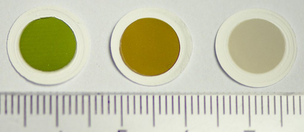
A method developed at Aalto University, Finland, can produce large quantities of pristine single-walled carbon nanotubes in select shades of the rainbow. The secret is a fine-tuned fabrication process—and a small dose of carbon dioxide. The films could find applications in touch screen technologies or as coating agents for new types of solar cells.
Samples of the colourful carbon nanotube thin films, as produced in the fabrication reactor. Image: Aalto University.
Single-walled carbon nanotubes, or sheets of one atom-thick layers of graphene rolled up into different sizes and shapes, have found many uses in electronics and new touch screen devices. By nature, carbon nanotubes are typically black or a dark grey.
In their new study published in the Journal of the American Chemical Society (JACS), Aalto University researchers present a way to control the fabrication of carbon nanotube thin films so that they display a variety of different colours—for instance, green, brown, or a silvery grey.
The researchers believe this is the first time that coloured carbon nanotubes have been produced by direct synthesis. Using their invention, the colour is induced straight away in the fabrication process, not by employing a range of purifying techniques on finished, synthesized tubes.
With direct synthesis, large quantities of clean sample materials can be produced while also avoiding damage to the product in the purifying process—which makes it the most attractive approach for applications.
‘In theory, these coloured thin films could be used to make touch screens with many different colours, or solar cells that display completely new types of optical properties,’ says Esko Kauppinen, Professor at Aalto University.
To get carbon structures to display colours is a feat in itself. The underlying techniques needed to enable the colouration also imply finely detailed control of the structure of the nanotube structures. Kauppinen and his team’s unique method, which uses aerosols of metal and carbon, allows them to carefully manipulate and control the nanotube structure directly from the fabrication process.
‘Growing carbon nanotubes is, in a way, like planting trees: we need seeds, feeds, and solar heat. For us, aerosol nanoparticles of iron work as a catalyst or seed, carbon monoxide as the source for carbon, so feed, and a reactor gives heat at a temperature more than 850 degrees Celsius,’ says Dr. Hua Jiang, Senior Scientist at Aalto University.
Professor Kauppinen’s group has a long history of using these very resources in their singular production method. To add to their repertoire, they have recently experimented with administering small doses of carbon dioxide into the fabrication process.
‘Carbon dioxide acts as a kind of graft material that we can use to tune the growth of carbon nanotubes of various colors,’ explains Jiang.
With an advanced electron diffraction technique, the researchers were able to find out the precise atomic scale structure of their thin films. They found that they have very narrow chirality distributions, meaning that the orientation of the honeycomb-lattice of the tubes’ walls is almost uniform throughout the sample. The chirality more or less dictates the electrical properties carbon nanotubes can have, as well as their colour.
The method developed at Aalto University promises a simple and highly scalable way to fabricate carbon nanotube thin films in high yields.
‘Usually you have to choose between mass production or having good control over the structure of carbon nanotubes. With our breakthrough, we can do both,’ trusts Dr. Qiang Zhang, a postdoctoral researcher in the group.
Follow-up work is already underway.
‘We want to understand the science of how the addition of carbon dioxide tunes the structure of the nanotubes and creates colours. Our aim is to achieve full control of the growing process so that single-walled carbon nanotubes could be used as building blocks for the next generation of nanoelectronics devices,’ says professor Kauppinen.
Here’s a link to and a citation for the paper,
Direct Synthesis of Colorful Single-Walled Carbon Nanotube Thin Films by Yongping Liao, Hua Jiang, Nan Wei, Patrik Laiho, Qiang Zhang, Sabbir A. Khan, and Esko I. Kauppinen. J. Am. Chem. Soc., 2018, 140 (31), pp 9797–9800 DOI: 10.1021/jacs.8b05151 Publication Date (Web): July 26, 2018
Base-pairing properties of DNA were used to construct tiny structures that accumulated a silica outer skeleton similar to shell-building organisms known as diatoms. Credit: Yan Lab. [downloaded from https://phys.org/news/2018-07-single-celled-architects-nanotechnology.html]
The gif below isn’t quite so pretty as the image above but it’s both an example of the kind of imagery (lots of grey), that scientists routinely work with and it shows the work in more detail,
3D cube made using DNA Origami Silicification (DOS), which deposits a fine layer of silica onto the DNA origami framework. Credit: Yan Lab [downloaded from https://phys.org/news/2018-07-single-celled-architects-nanotechnology.html]
Diatoms are tiny, unicellular creatures, inhabiting oceans, lakes, rivers, and soils. Through their respiration, they produce close to a quarter of the oxygen on earth, nearly as much as the world’s tropical forests. In addition to their ecological success across the planet, they have a number of remarkable properties. Diatoms live in glasslike homes of their own design, visible under magnification in an astonishing and aesthetically beautiful range of forms.
Researchers have found inspiration in these microscopic, jewel-like products of nature since their discovery in the late 18th century. In a new study, Arizona State University (ASU) scientists led by Professor Hao Yan, in collaboration with researchers from the Shanghai Institute of Applied Physics of the Chinese Academy of Sciences and Shanghai Jiaotong University led by Prof. Chunhai Fan, have designed a range of diatom-like nanostructures.
To achieve this, they borrow techniques used by naturally-occurring diatoms to deposit layers of silica—the primary constituent in glass—in order to grow their intricate shells. Using a technique known as DNA origami, the group designed nanoscale platforms of various shapes to which particles of silica, drawn by electrical charge, could stick.
The new research demonstrates that silica deposition can be effectively applied to synthetic, DNA-based architectures, improving their elasticity and durability. The work could ultimately have far-reaching applications in new optical systems, semiconductor nanolithography, nano-electronics, nano-robotics and medical applications, including drug delivery.
…
Researchers like Yan and Fan create sophisticated nanoarchitectures in 2- and 3-dimensions, using DNA as a building material. The method, known as DNA origami, relies on the base-pairing properties of DNA’s four nucleotides, whose names are abbreviated A,T,C and G.
The ladder-like structure of the DNA double-helix is formed when complementary strands of nucleotides bond with each other—the C nucleotides always pairing with Gs and the As always pairing with Ts. This predictable behavior can be exploited in order to produce a virtually limitless variety of engineered shapes, which can be designed in advance. The nanostructures then self-assemble in a test tube.
In the new study, researchers wanted to see if architectures designed with DNA, each measuring just billionths of a meter in diameter, could be used as structural frameworks on which diatom-like exoskeletons composed of silica could grow in a precise and controllable manner. Their successful results show the power of this hybrid marriage of nature and nanoengineering, which the authors call DNA Origami Silicification (DOS).
“Here, we demonstrated that the right chemistry can be developed to produce DNA-silica hybrid materials that faithfully replicate the complex geometric information of a wide range of different DNA origami scaffolds. Our findings established a general method for creating biomimetic silica nanostructures,” said Yan.
Among the geometric DNA frameworks designed and constructed in the experiments were 2D crosses, squares, triangles and DOS-diatom honeycomb shapes as well as 3D cubes, tetrahedrons, hemispheres, toroid and ellipsoid forms, occurring as single units or lattices.
Once the DNA frameworks were complete, clusters of silica particles carrying a positive charge were drawn electrostatically to the surfaces of the electrically negative DNA shapes, accreting over a period of several days, like fine paint applied to an eggshell. A series of transmission- and scanning electron micrographs were made of the resulting DOS forms, revealing accurate and efficient diatom-like silicification.
The method proved effective for silicification of framelike, curved and porous nanostructures ranging in size from 10-1000 nanometers, (the largest structures are roughly the size of bacteria). Precise control over silica shell thickness is achieved simply by regulating the duration of growth.
The hybrid DOS-diatom nanostructures were initially characterized using a pair of powerful tools capable of unveiling their tiny forms, Transmission Electron Microscopy (TEM) and Atomic Force Microscopy (AFM). The resulting images reveal much clearer outlines for the nanostructures after the deposition of silica.
The method of nanofabrication is so precise, researchers were able to produce triangles, squares and hexagons with uniform pores measuring less than 10 nm in diameter—by far the smallest achieved to date, using DNA origami lithography. Further, the technique outlined in the new study equips researchers with more accurate control over the construction of 3D nanostructures in arbitrary forms that are often challenging to produce through existing methods.
One property of natural diatoms of great interests to nanoengineers like Yan and Fan is the specific strength of their silica shells. Specific strength refers to a material’s resistance to breakage relative to its density. Scientists have found that the silica architectures of diatoms are not only inspiringly elegant but exceptionally tough. Indeed, the silica exoskeletons enveloping diatoms have the highest specific strength of any biologically produced material, including bone, antlers, and teeth.
In the current study, researchers used AFM to measure the resistance to breakage of their silica-augmented DNA nanostructures. Like their natural counterparts, these forms showed far greater strength and resilience, displaying a 10-fold increase in the forces they could withstand, compared with the unsilicated designs, while nevertheless retaining considerable flexibility.
The study also shows that the enhanced rigidity of DOS nanostructures increases with their growth time. As the authors note, these results are in agreement with the characteristic mechanical properties of biominerals produced by nature, coupling impressive durability with flexibility.
A final experiment involved the design of a new 3D tetrahedral nanostructure using gold nanorods as supportive struts for a DOS fabricated device. This novel structure was able to faithfully retain its shape compared with a similar structure lacking silication that deformed and collapsed.
The research opens a pathway for nature-inspired innovations in nanotechnology in which DNA architectures act as templates that may be coated with silica or perhaps other inorganic materials, including calcium phosphate, calcium carbonate, ferric oxide or other metal oxides, yielding unique properties.
“We are interested in developing methods to create higher order hybrid nanostructures. For example, multi-layered/multi-component hybrid materials may be achieved by a stepwise deposition of different materials to further expand the biomimetic diversity,” said Fan.
Such capabilities will open up new opportunities to engineer highly programmable solid-state nanopores with hierarchical features, new porous materials with designed structural periodicity, cavity and functionality, plasmonic and meta-materials. The bio-inspired and biomimetic approach demonstrated in this paper represents a general framework for use with inorganic device nanofabrication that has arbitrary 3D shapes and functions and offers diverse potential applications in fields such as nano-electronics, nano-photonics, and nano-robotics.
Here’s a link to and a citation for the paper,
Complex silica composite nanomaterials templated with DNA origami by Xiaoguo Liu, Fei Zhang, Xinxin Jing, Muchen Pan, Pi Liu, Wei Li, Bowen Zhu, Jiang Li, Hong Chen, Lihua Wang, Jianping Lin, Yan Liu, Dongyuan Zhao, Hao Yan, & Chunhai Fan. Nature (2018) DOI: https://doi.org/10.1038/s41586-018-0332-7 Published 16 July 2018
Libraries, archives, records management, oral history, etc. there are many institutions and names for how we manage collective and personal memory. You might call it a peculiarly human obsession stretching back into antiquity. For example, there’s the Library of Alexandria (Wikipedia entry) founded in the third, or possibly 2nd, century BCE (before the common era) and reputed to store all the knowledge in the world. It was destroyed although accounts differ as to when and how but its loss remains a potent reminder of memory’s fragility.
These days, the technology community is terribly concerned with storing ever more bits of data on materials that are reaching their limits for storage.I have news of a possible solution, an interview of sorts with the researchers working on this new technology, and some very recent research into policies for cryptocurrency mining and development. That bit about cryptocurrency makes more sense when you read what the response to one of the interview questions.
Memory
It seems University of Alberta researchers may have found a way to increase memory exponentially, from a July 23, 2018 news item on ScienceDaily,
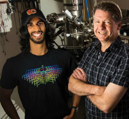
The most dense solid-state memory ever created could soon exceed the capabilities of current computer storage devices by 1,000 times, thanks to a new technique scientists at the University of Alberta have perfected.
“Essentially, you can take all 45 million songs on iTunes and store them on the surface of one quarter,” said Roshan Achal, PhD student in Department of Physics and lead author on the new research. “Five years ago, this wasn’t even something we thought possible.”
Previous discoveries were stable only at cryogenic conditions, meaning this new finding puts society light years closer to meeting the need for more storage for the current and continued deluge of data. One of the most exciting features of this memory is that it’s road-ready for real-world temperatures, as it can withstand normal use and transportation beyond the lab.
“What is often overlooked in the nanofabrication business is actual transportation to an end user, that simply was not possible until now given temperature restrictions,” continued Achal. “Our memory is stable well above room temperature and precise down to the atom.”
Achal explained that immediate applications will be data archival. Next steps will be increasing readout and writing speeds, meaning even more flexible applications.
“With this last piece of the puzzle now in-hand, atom-scale fabrication will become a commercial reality in the very near future,” said Wolkow. Wolkow’s Spin-off [sic] company, Quantum Silicon Inc., is hard at work on commercializing atom-scale fabrication for use in all areas of the technology sector.
To demonstrate the new discovery, Achal, Wolkow, and their fellow scientists not only fabricated the world’s smallest maple leaf, they also encoded the entire alphabet at a density of 138 terabytes, roughly equivalent to writing 350,000 letters across a grain of rice. For a playful twist, Achal also encoded music as an atom-sized song, the first 24 notes of which will make any video-game player of the 80s and 90s nostalgic for yesteryear but excited for the future of technology and society.
As noted in the news release, there is an atom-sized song, which is available in this video,
As for the nano-sized maple leaf, I highlighted that bit of whimsy in a June 30, 2017 posting.
Here’s a link to and a citation for the paper,
Lithography for robust and editable atomic-scale silicon devices and memories by Roshan Achal, Mohammad Rashidi, Jeremiah Croshaw, David Churchill, Marco Taucer, Taleana Huff, Martin Cloutier, Jason Pitters, & Robert A. Wolkow. Nature Communicationsvolume 9, Article number: 2778 (2018) DOI: https://doi.org/10.1038/s41467-018-05171-y Published 23 July 2018
This paper is open access.
For interested parties, you can find Quantum Silicon (QSI) here. My Edmonton geography is all but nonexistent, still, it seems to me the company address on Saskatchewan Drive is a University of Alberta address. It’s also the address for the National Research Council of Canada. Perhaps this is a university/government spin-off company?
The ‘interview’
I sent some questions to the researchers at the University of Alberta who very kindly provided me with the following answers. Roshan Achal passed on one of the questions to his colleague Taleana Huff for her response. Both Achal and Huff are associated with QSI.
Unfortunately I could not find any pictures of all three researchers (Achal, Huff, and Wolkow) together.
Roshan Achal (left) used nanotechnology perfected by his PhD supervisor, Robert Wolkow (right) to create atomic-scale computer memory that could exceed the capacity of today’s solid-state storage drives by 1,000 times. (Photo: Faculty of Science)
(1) SHRINKING THE MANUFACTURING PROCESS TO THE ATOMIC SCALE HAS
ATTRACTED A LOT OF ATTENTION OVER THE YEARS STARTING WITH SCIENCE
FICTION OR RICHARD FEYNMAN OR K. ERIC DREXLER, ETC. IN ANY EVENT, THE
ORIGINS ARE CONTESTED SO I WON’T PUT YOU ON THE SPOT BY ASKING WHO
STARTED IT ALL INSTEAD ASKING HOW DID YOU GET STARTED?
I got started in this field about 6 years ago, when I undertook a MSc
with Dr. Wolkow here at the University of Alberta. Before that point, I
had only ever heard of a scanning tunneling microscope from what was
taught in my classes. I was aware of the famous IBM logo made up from
just a handful of atoms using this machine, but I didn’t know what
else could be done. Here, Dr. Wolkow introduced me to his line of
research, and I saw the immense potential for growth in this area and
decided to pursue it further. I had the chance to interact with and
learn from nanofabrication experts and gain the skills necessary to
begin playing around with my own techniques and ideas during my PhD.
(2) AS I UNDERSTAND IT, THESE ARE THE PIECES YOU’VE BEEN
WORKING ON: (1) THE TUNGSTEN MICROSCOPE TIP, WHICH MAKE[s] (2) THE SMALLEST
QUANTUM DOTS (SINGLE ATOMS OF SILICON), (3) THE AUTOMATION OF THE
QUANTUM DOT PRODUCTION PROCESS, AND (4) THE “MOST DENSE SOLID-STATE
MEMORY EVER CREATED.” WHAT’S MISSING FROM THE LIST AND IS THAT WHAT
YOU’RE WORKING ON NOW?
One of the things missing from the list, that we are currently working
on, is the ability to easily communicate (electrically) from the
macroscale (our world) to the nanoscale, without the use of a scanning
tunneling microscope. With this, we would be able to then construct
devices using the other pieces we’ve developed up to this point, and
then integrate them with more conventional electronics. This would bring
us yet another step closer to the realization of atomic-scale
electronics.
(3) PERHAPS YOU COULD CLARIFY SOMETHING FOR ME. USUALLY WHEN SOLID STATE
MEMORY IS MENTIONED, THERE’S GREAT CONCERN ABOUT MOORE’S LAW. IS
THIS WORK GOING TO CREATE A NEW LAW? AND, WHAT IF ANYTHING DOES
;YOUR MEMORY DEVICE HAVE TO DO WITH QUANTUM COMPUTING?
That is an interesting question. With the density we’ve achieved,
there are not too many surfaces where atomic sites are more closely
spaced to allow for another factor of two improvement. In that sense, it
would be difficult to improve memory densities further using these
techniques alone. In order to continue Moore’s law, new techniques, or
storage methods would have to be developed to move beyond atomic-scale
storage.
The memory design itself does not have anything to do with quantum
computing, however, the lithographic techniques developed through our
work, may enable the development of certain quantum-dot-based quantum
computing schemes.
(4) THIS MAY BE A LITTLE OUT OF LEFT FIELD (OR FURTHER OUT THAN THE
OTHERS), COULD;YOUR MEMORY DEVICE HAVE AN IMPACT ON THE
DEVELOPMENT OF CRYPTOCURRENCY AND BLOCKCHAIN? IF SO, WHAT MIGHT THAT
IMPACT BE?
I am not very familiar with these topics, however, co-author Taleana
Huff has provided some thoughts:
Taleana Huff (downloaded from https://ca.linkedin.com/in/taleana-huff]
“The memory, as we’ve designed it, might not have too much of an
impact in and of itself. Cryptocurrencies fall into two categories.
Proof of Work and Proof of Stake. Proof of Work relies on raw
computational power to solve a difficult math problem. If you solve it,
you get rewarded with a small amount of that coin. The problem is that
it can take a lot of power and energy for your computer to crunch
through that problem. Faster access to memory alone could perhaps
streamline small parts of this slightly, but it would be very slight.
Proof of Stake is already quite power efficient and wouldn’t really
have a drastic advantage from better faster computers.
Now, atomic-scale circuitry built using these new lithographic
techniques that we’ve developed, which could perform computations at
significantly lower energy costs, would be huge for Proof of Work coins.
One of the things holding bitcoin back, for example, is that mining it
is now consuming power on the order of the annual energy consumption
required by small countries. A more efficient way to mine while still
taking the same amount of time to solve the problem would make bitcoin
much more attractive as a currency.”
Thank you to Roshan Achal and Taleana Huff for helping me to further explore the implications of their work with Dr. Wolkow.
Comments
As usual, after receiving the replies I have more questions but these people have other things to do so I’ll content myself with noting that there is something extraordinary in the fact that we can imagine a near future where atomic scale manufacturing is possible and where as Achal says, ” … storage methods would have to be developed to move beyond atomic-scale [emphasis mine] storage”. In decades past it was the stuff of science fiction or of theorists who didn’t have the tools to turn the idea into a reality. With Wolkow’s, Achal’s, Hauff’s, and their colleagues’ work, atomic scale manufacturing is attainable in the foreseeable future.
Hopefully we’ll be wiser than we have been in the past in how we deploy these new manufacturing techniques. Of course, before we need the wisdom, scientists, as Achal notes, need to find a new way to communicate between the macroscale and the nanoscale.
As for Huff’s comments about cryptocurrencies and cyptocurrency and blockchain technology, I stumbled across this very recent research, from a July 31, 2018 Elsevier press release (also on EurekAlert),
A study [behind a paywall] published in Energy Research & Social Science warns that failure to lower the energy use by Bitcoin and similar Blockchain designs may prevent nations from reaching their climate change mitigation obligations under the Paris Agreement.
The study, authored by Jon Truby, PhD, Assistant Professor, Director of the Centre for Law & Development, College of Law, Qatar University, Doha, Qatar, evaluates the financial and legal options available to lawmakers to moderate blockchain-related energy consumption and foster a sustainable and innovative technology sector. Based on this rigorous review and analysis of the technologies, ownership models, and jurisdictional case law and practices, the article recommends an approach that imposes new taxes, charges, or restrictions to reduce demand by users, miners, and miner manufacturers who employ polluting technologies, and offers incentives that encourage developers to create less energy-intensive/carbon-neutral Blockchain.
“Digital currency mining is the first major industry developed from Blockchain, because its transactions alone consume more electricity than entire nations,” said Dr. Truby. “It needs to be directed towards sustainability if it is to realize its potential advantages.
“Many developers have taken no account of the environmental impact of their designs, so we must encourage them to adopt consensus protocols that do not result in high emissions. Taking no action means we are subsidizing high energy-consuming technology and causing future Blockchain developers to follow the same harmful path. We need to de-socialize the environmental costs involved while continuing to encourage progress of this important technology to unlock its potential economic, environmental, and social benefits,” explained Dr. Truby.
As a digital ledger that is accessible to, and trusted by all participants, Blockchain technology decentralizes and transforms the exchange of assets through peer-to-peer verification and payments. Blockchain technology has been advocated as being capable of delivering environmental and social benefits under the UN’s Sustainable Development Goals. However, Bitcoin’s system has been built in a way that is reminiscent of physical mining of natural resources – costs and efforts rise as the system reaches the ultimate resource limit and the mining of new resources requires increasing hardware resources, which consume huge amounts of electricity.
Putting this into perspective, Dr. Truby said, “the processes involved in a single Bitcoin transaction could provide electricity to a British home for a month – with the environmental costs socialized for private benefit.
“Bitcoin is here to stay, and so, future models must be designed without reliance on energy consumption so disproportionate on their economic or social benefits.”
The study evaluates various Blockchain technologies by their carbon footprints and recommends how to tax or restrict Blockchain types at different phases of production and use to discourage polluting versions and encourage cleaner alternatives. It also analyzes the legal measures that can be introduced to encourage technology innovators to develop low-emissions Blockchain designs. The specific recommendations include imposing levies to prevent path-dependent inertia from constraining innovation:
Registration fees collected by brokers from digital coin buyers.
“Bitcoin Sin Tax” surcharge on digital currency ownership.
Green taxes and restrictions on machinery purchases/imports (e.g. Bitcoin mining machines).
Smart contract transaction charges.
According to Dr. Truby, these findings may lead to new taxes, charges or restrictions, but could also lead to financial rewards for innovators developing carbon-neutral Blockchain.
The press release doesn’t fully reflect Dr. Truby’s thoughtfulness or the incentives he has suggested. it’s not all surcharges, taxes, and fees constitute encouragement. Here’s a sample from the conclusion,
The possibilities of Blockchain are endless and incentivisation can help solve various climate change issues, such as through the development of digital currencies to fund climate finance programmes. This type of public-private finance initiative is envisioned in the Paris Agreement, and fiscal tools can incentivize innovators to design financially rewarding Blockchain technology that also achieves environmental goals. Bitcoin, for example, has various utilitarian intentions in its White Paper, which may or may not turn out to be as envisioned, but it would not have been such a success without investors seeking remarkable returns. Embracing such technology, and promoting a shift in behaviour with such fiscal tools, can turn the industry itself towards achieving innovative solutions for environmental goals.
I realize Wolkow, et. al, are not focused on cryptocurrency and blockchain technology per se but as Huff notes in her reply, “… new lithographic techniques that we’ve developed, which could perform computations at significantly lower energy costs, would be huge for Proof of Work coins.”
Whether or not there are implications for cryptocurrencies, energy needs, climate change, etc., it’s the kind of innovative work being done by scientists at the University of Alberta which may have implications in fields far beyond the researchers’ original intentions such as more efficient computation and data storage.
ETA Aug. 6, 2018: Dexter Johnson weighed in with an August 3, 2018 posting on his Nanoclast blog (on the IEEE [Institute of Electrical and Electronics Engineers] website),
Researchers at the University of Alberta in Canada have developed a new approach to rewritable data storage technology by using a scanning tunneling microscope (STM) to remove and replace hydrogen atoms from the surface of a silicon wafer. If this approach realizes its potential, it could lead to a data storage technology capable of storing 1,000 times more data than today’s hard drives, up to 138 terabytes per square inch.
As a bit of background, Gerd Binnig and Heinrich Rohrer developed the first STM in 1986 for which they later received the Nobel Prize in physics. In the over 30 years since an STM first imaged an atom by exploiting a phenomenon known as tunneling—which causes electrons to jump from the surface atoms of a material to the tip of an ultrasharp electrode suspended a few angstroms above—the technology has become the backbone of so-called nanotechnology.
In addition to imaging the world on the atomic scale for the last thirty years, STMs have been experimented with as a potential data storage device. Last year, we reported on how IBM (where Binnig and Rohrer first developed the STM) used an STM in combination with an iron atom to serve as an electron-spin resonance sensor to read the magnetic pole of holmium atoms. The north and south poles of the holmium atoms served as the 0 and 1 of digital logic.
The Canadian researchers have taken a somewhat different approach to making an STM into a data storage device by automating a known technique that uses the ultrasharp tip of the STM to apply a voltage pulse above an atom to remove individual hydrogen atoms from the surface of a silicon wafer. Once the atom has been removed, there is a vacancy on the surface. These vacancies can be patterned on the surface to create devices and memories.
If you have the time, I recommend reading Dexter’s posting as he provides clear explanations, additional insight into the work, and more historical detail.
… the path to greater benefits – whether economic, social, or environmental – from nanomanufactured goods and services is not yet clear. A recent review article in ACS Nano (“Nanomanufacturing: A Perspective”) by J. Alexander Liddle and Gregg M. Gallatin, takes silicon integrated circuit manufacturing as a baseline in order to consider the factors involved in matching processes with products, examining the characteristics and potential of top-down and bottom-up processes, and their combination.
The authors also discuss how a careful assessment of the way in which function can be made to follow form can enable high-volume manufacturing of nanoscale structures with the desired useful, and exciting, properties.
Although often used interchangeably, it makes sense to distinguish between nanofabrication and nanomanufacturing using the criterion of economic viability, suggested by the connotations of industrial scale and profitability associated with the word ‘manufacturing’.
Here’s a link to and a citation for the paper Berger is reviewing,
Nanomanufacturing: A Perspective by J. Alexander Liddle and Gregg M. Gallatin. ACS Nano, 2016, 10 (3), pp 2995–3014 DOI: 10.1021/acsnano.5b03299 Publication Date (Web): February 10, 2016
Copyright This article not subject to U.S. Copyright. Published 2016 by the American Chemical Society
This paper is behind a paywall.
Luckily for those who’d like a little more information before purchase, Berger’s review provides some insight into the study additional to what you’ll find in the abstract,
Nanomanufacturing, as the authors define it in their article, therefore, has the salient characteristic of being a source of money, while nanofabrication is often a sink.
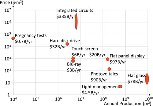
To supply some background and indicate the scale of the nanomanufacturing challenge, the figure below shows the selling price ($·m-2) versus the annual production (m2) for a variety of nanoenabled or potentially nanoenabled products. The overall global market sizes are also indicated. It is interesting to note that the selling price spans 5 orders of magnitude, the production six, and the market size three. Although there is no strong correlation between the variables,
market price and size nanoenabled product
Log-log plot of the approximate product selling price ($·m-2) versus global annual production (m2) for a variety of nanoenabled, or potentially nanoenabled products. Approximate market sizes (2014) are shown next to each point. (Reprinted with permission by American Chemical Society)
Log-log plot of the approximate product selling price ($·m-2) versus global annual production (m2) for a variety of nanoenabled, or potentially nanoenabled products. Approximate market sizes (2014) are shown next to each point. (Reprinted with permission by American Chemical Society)
I encourage anyone interested in nanomanufacturing to read Berger’s article in its entirety as there is more detail and there are more figures to illustrate the points being made. He ends his review with this,
“Perhaps the most exciting prospect is that of creating dynamical nanoscale systems that are capable of exhibiting much richer structures and functionality. Whether this is achieved by learning how to control and engineer biological systems directly, or by building systems based on the same principles, remains to be seen, but will undoubtedly be disruptive and quite probably revolutionary.”
I find the reference to biological systems quite interesting especially in light of the recent launch of DARPA’s (US Defense Advanced Research Projects Agency) Engineered Living Materials (ELM) program (see my Aug. 9, 2016 posting).
A Jan. 6, 2015 news item on Nanowerk features a proposal by US scientists for a Unified Microbiome Initiative (UMI),
In October [2015], an interdisciplinary group of scientists proposed forming a Unified Microbiome Initiative (UMI) to explore the world of microorganisms that are central to life on Earth and yet largely remain a mystery.
An article in the journal ACS Nano (“Tools for the Microbiome: Nano and Beyond”) describes the tools scientists will need to understand how microbes interact with each other and with us.
Microbes live just about everywhere: in the oceans, in the soil, in the atmosphere, in forests and in and on our bodies. Research has demonstrated that their influence ranges widely and profoundly, from affecting human health to the climate. But scientists don’t have the necessary tools to characterize communities of microbes, called microbiomes, and how they function. Rob Knight, Jeff F. Miller, Paul S. Weiss and colleagues detail what these technological needs are.
The researchers are seeking the development of advanced tools in bioinformatics, high-resolution imaging, and the sequencing of microbial macromolecules and metabolites. They say that such technology would enable scientists to gain a deeper understanding of microbiomes. Armed with new knowledge, they could then tackle related medical and other challenges with greater agility than what is possible today.
Here’s a link to and a citation for the paper,
Tools for the Microbiome: Nano and Beyond by Julie S. Biteen, Paul C. Blainey, Zoe G. Cardon, Miyoung Chun, George M. Church, Pieter C. Dorrestein, Scott E. Fraser, Jack A. Gilbert, Janet K. Jansson, Rob Knight, Jeff F. Miller, Aydogan Ozcan, Kimberly A. Prather, Stephen R. Quake, Edward G. Ruby, Pamela A. Silver, Sharif Taha, Ger van den Engh, Paul S. Weiss, Gerard C. L. Wong, Aaron T. Wright, and Thomas D. Young. ACS Nano, Article ASAP DOI: 10.1021/acsnano.5b07826 Publication Date (Web): December 22, 2015
I sped through very quickly and found a couple of references to ‘nano’,
Ocean Microbiomes and Nanobiomes
Life in the oceans is supported by a community of extremely small organisms that can be called a “nanobiome.” These nanoplankton particles, many of which measure less than 0.001× the volume of a white blood cell, harvest solar and chemical energy and channel essential elements into the food chain. A deep network of larger life forms (humans included) depends on these tiny microbes for its energy and chemical building blocks.
The importance of the oceanic nanobiome has only recently begun to be fully appreciated. Two dominant forms, Synechococcus and Prochlorococcus, were not discovered until the 1980s and 1990s.(32-34) Prochloroccus has now been demonstrated to be so abundant that it may account for as much as 10% of the world’s living organic carbon. The organism divides on a diel cycle while maintaining constant numbers, suggesting that about 5% of the world’s biomass flows through this species on a daily basis.(35-37)
Metagenomic studies show that many other less abundant life forms must exist but elude direct observation because they can neither be isolated nor grown in culture.
The small sizes of these organisms (and their genomes) indicate that they are highly specialized and optimized. Metagenome data indicate a large metabolic heterogeneity within the nanobiome. Rather than combining all life functions into a single organism, the nanobiome works as a network of specialists that can only exist as a community, therein explaining their resistance to being cultured. The detailed composition of the network is the result of interactions between the organisms themselves and the local physical and chemical environment. There is thus far little insight into how these networks are formed and how they maintain steady-state conditions in the turbulent natural ocean environment.
Rather than combining all life functions into a single organism, the nanobiome works as a network of specialists that can only exist as a community
The serendipitous discovery of Prochlorococcus happened by applying flow cytometry (developed as a medical technique for counting blood cells) to seawater.(34) With these medical instruments, the faint signals from nanoplankton can only be seen with great difficulty against noisy backgrounds. Currently, a small team is adapting flow cytometric technology to improve the capabilities for analyzing individual nanoplankton particles. The latest generation of flow cytometers enables researchers to count and to make quantitative observations of most of the small life forms (including some viruses) that comprise the nanobiome. To our knowledge, there are only two well-equipped mobile flow cytometry laboratories that are regularly taken to sea for real-time observations of the nanobiome. The laboratories include equipment for (meta)genome analysis and equipment to correlate the observations with the local physical parameters and (nutrient) chemistry in the ocean. Ultimately, integration of these measurements will be essential for understanding the complexity of the oceanic microbiome.
The ocean is tremendously undersampled. Ship time is costly and limited. Ultimately, inexpensive, automated, mobile biome observatories will require methods that integrate microbiome and nanobiome measurements, with (meta-) genomics analyses, with local geophysical and geochemical parameters.(38-42) To appreciate how the individual components of the ocean biome are related and work together, a more complete picture must be established.
The marine environment consists of stratified zones, each with a unique, characteristic biome.(43) The sunlit waters near the surface are mixed by wind action. Deeper waters may be mixed only occasionally by passing storms. The dark deepest layers are stabilized by temperature/salinity density gradients. Organic material from the photosynthetically active surface descends into the deep zone, where it decomposes into nutrients that are mixed with compounds that are released by volcanic and seismic action. These nutrients diffuse upward to replenish the depleted surface waters. The biome is stratified accordingly, sometimes with sudden transitions on small scales. Photo-autotrophs dominate near the surface. Chemo-heterotrophs populate the deep. The makeup of the microbial assemblages is dictated by the local nutrient and oxygen concentrations. The spatiotemporal interplay of these systems is highly relevant to such issues as the carbon budget of the planet but remains little understood.
And then, there was this,
Nanoscience and Nanotechnology Opportunities
The great advantage of nanoscience and nanotechnology in studying microbiomes is that the nanoscale is the scale of function in biology. It is this convergence of scales at which we can “see” and at which we can fabricate that heralds the contributions that can be made by developing new nanoscale analysis tools.(159-168) Microbiomes operate from the nanoscale up to much larger scales, even kilometers, so crossing these scales will pose significant challenges to the field, in terms of measurement, stimulation/response, informatics, and ultimately understanding.
Some progress has been made in creating model systems(143-145, 169-173) that can be used to develop tools and methods. In these cases, the tools can be brought to bear on more complex and real systems. Just as nanoscience began with the ability to image atoms and progressed to the ability to manipulate structures both directly and through guided interactions,(162, 163, 174-176) it has now become possible to control structure, materials, and chemical functionality from the submolecular to the centimeter scales simultaneously. Whereas substrates and surface functionalization have often been tailored to be resistant to bioadhesion, deliberate placement of chemical patterns can also be used for the growth and patterning of systems, such as biofilms, to be put into contact with nanoscale probes.(177-180) Such methods in combination with the tools of other fields (vide infra) will provide the means to probe and to understand microbiomes.
Key tools for the microbiome will need to be miniaturized and made parallel. These developments will leverage decades of work in nanotechnology in the areas of nanofabrication,(181) imaging systems,(182, 183) lab-on-a-chip systems,(184) control of biological interfaces,(185) and more. Commercialized and commoditized tools, such as smart phone cameras, can also be adapted for use (vide infra). By guiding the development and parallelization of these tools, increasingly complex microbiomes will be opened for study.(167)
Imaging and sensing, in general, have been enjoying a Renaissance over the past decades, and there are various powerful measurement techniques that are currently available, making the Microbiome Initiative timely and exciting from the broad perspective of advanced analysis techniques. Recent advances in various -omics technologies, electron microscopy, optical microscopy/nanoscopy and spectroscopy, cytometry, mass spectroscopy, atomic force microscopy, nuclear imaging, and other techniques, create unique opportunities for researchers to investigate a wide range of questions related to microbiome interactions, function, and diversity. We anticipate that some of these advanced imaging, spectroscopy, and sensing techniques, coupled with big data analytics, will be used to create multimodal and integrated smart systems that can shed light onto some of the most important needs in microbiome research, including (1) analyzing microbial interactions specifically and sensitively at the relevant spatial and temporal scales; (2) determining and analyzing the diversity covered by the microbial genome, transcriptome, proteome, and metabolome; (3) managing and manipulating microbiomes to probe their function, evaluating the impact of interventions and ultimately harnessing their activities; and (4) helping us identify and track microbial dark matter (referring to 99% of micro-organisms that cannot be cultured).
In this broad quest for creating next-generation imaging and sensing instrumentation to address the needs and challenges of microbiome-related research activities comprehensively, there are important issues that need to be considered, as discussed below.
The piece is extensive and quite interesting, if you have the time.
The US Air Force wants to merge classical and quantum physics for practical purposes according to a May 5, 2014 news item on Azonano,
The Air Force Office of Scientific Research has selected the Harvard School of Engineering and Applied Sciences (SEAS) to lead a multidisciplinary effort that will merge research in classical and quantum physics and accelerate the development of advanced optical technologies.
Federico Capasso, Robert L. Wallace Professor of Applied Physics and Vinton Hayes Senior Research Fellow in Electrical Engineering, will lead this Multidisciplinary University Research Initiative [MURI] with a world-class team of collaborators from Harvard, Columbia University, Purdue University, Stanford University, the University of Pennsylvania, Lund University, and the University of Southampton.
The grant is expected to advance physics and materials science in directions that could lead to very sophisticated lenses, communication technologies, quantum information devices, and imaging technologies.
“This is one of the world’s strongest possible teams,” said Capasso. “I am proud to lead this group of people, who are internationally renowned experts in their fields, and I believe we can really break new ground.”
The premise of nanophotonics is that light can interact with matter in unusual ways when the material incorporates tiny metallic or dielectric features that are separated by a distance shorter than the wavelength of the light. Metamaterials are engineered materials that exploit these phenomena, producing strange effects, enabling light to bend unnaturally, twist into a vortex, or disappear entirely. Yet the fabrication of thick, or bulk, metamaterials—that manipulate light as it passes through the material—has proven very challenging.
Recent research by Capasso and others in the field has demonstrated that with the right device structure, the critical manipulations can actually be confined to the very surface of the material—what they have dubbed a “metasurface.” These metasurfaces can impart an instantaneous shift in the phase, amplitude, and polarization of light, effectively controlling optical properties on demand. Importantly, they can be created in the lab using fairly common fabrication techniques.
At Harvard, the research has produced devices like an extremely thin, flat lens, and a material that absorbs 99.75% of infrared light. But, so far, such devices have been built to order—brilliantly suited to a single task, but not tunable.
This project, however,is focused on the future (Note: Links have been removed),
“Can we make a rapidly configurable metasurface so that we can change it in real time and quickly? That’s really a visionary frontier,” said Capasso. “We want to go all the way from the fundamental physics to the material building blocks and then the actual devices, to arrive at some sort of system demonstration.”
The proposed research also goes further. A key thrust of the project involves combining nanophotonics with research in quantum photonics. By exploiting the quantum effects of luminescent atomic impurities in diamond, for example, physicists and engineers have shown that light can be captured, stored, manipulated, and emitted as a controlled stream of single photons. These types of devices are essential building blocks for the realization of secure quantum communication systems and quantum computers. By coupling these quantum systems with metasurfaces—creating so-called quantum metasurfaces—the team believes it is possible to achieve an unprecedented level of control over the emission of photons.
“Just 20 years ago, the notion that photons could be manipulated at the subwavelength scale was thought to be some exotic thing, far fetched and of very limited use,” said Capasso. “But basic research opens up new avenues. In hindsight we know that new discoveries tend to lead to other technology developments in unexpected ways.”
The research team includes experts in theoretical physics, metamaterials, nanophotonic circuitry, quantum devices, plasmonics, nanofabrication, and computational modeling. Co-principal investigator Marko Lončar is the Tiantsai Lin Professor of Electrical Engineering at Harvard SEAS. Co-PI Nanfang Yu, Ph.D. ’09, developed expertise in metasurfaces as a student in Capasso’s Harvard laboratory; he is now an assistant professor of applied physics at Columbia. Additional co-PIs include Alexandra Boltasseva and Vladimir Shalaev at Purdue, Mark Brongersma at Stanford, and Nader Engheta at the University of Pennsylvania. Lars Samuelson (Lund University) and Nikolay Zheludev (University of Southampton) will also participate.
The bulk of the funding will support talented graduate students at the lead institutions.
The project, titled “Active Metasurfaces for Advanced Wavefront Engineering and Waveguiding,” is among 24 planned MURI awards selected from 361 white papers and 88 detailed proposals evaluated by a panel of experts; each award is subject to successful negotiation. The anticipated amount of the Harvard-led grant is up to $6.5 million for three to five years.
For anyone who’s not familiar (that includes me, anyway) with MURI awards, there’s this from Wikipedia (Note: links have been removed),
Multidisciplinary University Research Initiative (MURI) is a basic research program sponsored by the US Department of Defense (DoD). Currently each MURI award is about $1.5 million a year for five years.
I gather that in addition to the Air Force, the Army and the Navy also award MURI funds.
Another Chad Mirkin, Northwestern University (Chicago, Illinois, US), research breakthrough has been announced (this man, with regard to research, is as prolific as a bunny) in a July 19, 2013 news item on ScienceDaily,
A new low-cost, high-resolution tool is primed to revolutionize how nanotechnology is produced from the desktop, according to a new study by Northwestern University researchers.
Currently, most nanofabrication is done in multibillion-dollar centralized facilities called foundries. This is similar to printing documents in centralized printing shops. Consider, however, how the desktop printer revolutionized the transfer of information by allowing individuals to inexpensively print documents as needed. This paradigm shift is why there has been community-wide ambition in the field of nanoscience to create a desktop nanofabrication tool.
“With this breakthrough, we can construct very high-quality materials and devices, such as processing semiconductors over large areas, and we can do it with an instrument slightly larger than a printer,” said Chad A. Mirkin, senior author of the study.
The July 19, 2013 Northwestern University news release (on EurekAlert), which originated the news item, provides details,
The tool Mirkin’s team has created produces working devices and structures at the nanoscale level in a matter of hours, right at the point of use. It is the nanofabrication equivalent of a desktop printer.
Without requiring millions of dollars in instrumentation costs, the tool is poised to prototype a diverse range of functional structures, from gene chips to protein arrays to building patterns that control how stem cells differentiate to making electronic circuits.
“Instead of needing to have access to millions of dollars, in some cases billions of dollars of instrumentation, you can begin to build devices that normally require that type of instrumentation right at the point of use,” Mirkin said.
The paper details the advances Mirkin’s team has made in desktop nanofabrication based upon easily fabricated beam-pen lithography (BPL) pen arrays, structures that consist of an array of polymeric pyramids, each coated with an opaque layer with a 100 nanometer aperture at the tip. Using a digital micromirror device, the functional component of a projector, a single beam of light is broken up into thousands of individual beams, each channeled down the back of different pyramidal pens within the array and through the apertures at the tip of each pen.
The nanofabrication tool allows one to rapidly process substrates coated with photosensitive materials called resists and generate structures that span the macro-, micro- and nanoscales, all in one experiment.
Key advances made by Mirkin’s team include developing the hardware, writing the software to coordinate the direction of light onto the pen array and constructing a system to make all of the pieces of this instrument work together in synchrony. This approach allows each pen to write a unique pattern and for these patterns to be stitched together into functional devices.
“There is no need to create a mask or master plate every time you want to create a new structure,” Mirkin said. “You just assign the beams of light to go in different places and tell the pens what pattern you want generated.”
Because the materials used to make the desktop nanofabrication tool are easily accessible, commercialization may be as little as two years away, Mirkin said. In the meantime, his team is working on building more devices and prototypes.
In the paper, Mirkin explains how his lab produced a map of the world, with nanoscale resolution that is large enough to see with the naked eye, a feat never before achieved with a scanning probe instrument. Not only that, but closer inspection with a microscope reveals that this image is actually a mosaic of individual chemical formulae made up of nanoscale points. Making this pattern showcases the instrument’s capability of simultaneously writing centimeter-scale patterns with nanoscale resolution.
Here’s a link to and a citation for the published paper,
This paper is behind a paywall. As an alternative of sorts, you might like to check out this March 22, 2012 video of Mirkin’s presentation entitled, A Chemist’s Approach to Nanofabrication: Towards a “Desktop Fab” for the US Air Force Office of Scientific Research.
30 graduate students from across Canada came to the University of Toronto (U of T) this month (June 2011) to spend nine days learning how to make nano-sized devices. From the June 22, 2011 news item on Nanowerk,
The summer institute was conceived by Professor Stewart Aitchison of electrical and computer engineering, and was hosted by U of T’s ECTI (Emerging Communications Technology Institute), which provides open research facilities for micro- and nanofabrication. Funding was received from the University’s Connaught Fund to foster connections and collaborations among students, postdoctoral fellows and other scholars.
In six three-hour lab sessions, students learned how to operate equipment and perform the processes crucial to fabricating nano-scale devices. Aju Jugessur, a senior research associate with the ECTI, was part of the planning committee for the summer institute, and helped develop the training sessions.
…
The unique nature of the training is what attracted Rahul Lodha, a doctoral student in materials engineering from the University of British Columbia.
“I’m currently working with both micro- and nano-size particles, and what I’ve been doing is to add the nano-particles to micro-structures. What I’ve learned here is how to combine the two,” said Lodha. “What’s of great interest to me is how the properties of a material change when you get to the nano scale. Nano-titanium dioxide can be used for water purification, because when regular light hits it, ultra-violet rays are emitted in the range required to purify water. But regular sized titanium dioxide by itself doesn’t do this.”
It’s exciting when discoveries and innovations are coming fast and furious but it can be difficult to figure out exactly how to proceed. I just read about a new table-top technique for nanofabrication that doesn’t require ultra-violet light. This stands in contrast to the proposed new maskwriting facility for nanofrabrication at Simon Fraser University (SFU). The processes described in the SFU release and in the article about the table-top technique for lithographic patterning seem very similar except one uses ultra violet-light and the other does not. At this pace it seems as if the SFU facility is likely to beocme obsolete soon. Still, it’s a long way from experiments in a laboratory to industrial use as planned at SFU and I don’t imagine that it makes much sense to wait for the new process. After all by the time that’s ready for ‘prime time’ use, there’ll probably be another discovery.