Tag Archives: scanning tunneling microscope

More memory, less space and a walk down the cryptocurrency road

Libraries, archives, records management, oral history, etc. there are many institutions and names for how we manage collective and personal memory. You might call it a peculiarly human obsession stretching back into antiquity. For example, there’s the Library of Alexandria (Wikipedia entry) founded in the third, or possibly 2nd, century BCE (before the common era) and reputed to store all the knowledge in the world. It was destroyed although accounts differ as to when and how but its loss remains a potent reminder of memory’s fragility.

These days, the technology community is terribly concerned with storing ever more bits of data on materials that are reaching their limits for storage.I have news of a possible solution,  an interview of sorts with the researchers working on this new technology, and some very recent research into policies for cryptocurrency mining and development. That bit about cryptocurrency makes more sense when you read what the response to one of the interview questions.

Memory

It seems University of Alberta researchers may have found a way to increase memory exponentially, from a July 23, 2018 news item on ScienceDaily,

The most dense solid-state memory ever created could soon exceed the capabilities of current computer storage devices by 1,000 times, thanks to a new technique scientists at the University of Alberta have perfected.

“Essentially, you can take all 45 million songs on iTunes and store them on the surface of one quarter,” said Roshan Achal, PhD student in Department of Physics and lead author on the new research. “Five years ago, this wasn’t even something we thought possible.”

A July 23, 2018 University of Alberta news release (also on EurekAlert) by Jennifer-Anne Pascoe, which originated the news item, provides more information,

Previous discoveries were stable only at cryogenic conditions, meaning this new finding puts society light years closer to meeting the need for more storage for the current and continued deluge of data. One of the most exciting features of this memory is that it’s road-ready for real-world temperatures, as it can withstand normal use and transportation beyond the lab.

“What is often overlooked in the nanofabrication business is actual transportation to an end user, that simply was not possible until now given temperature restrictions,” continued Achal. “Our memory is stable well above room temperature and precise down to the atom.”

Achal explained that immediate applications will be data archival. Next steps will be increasing readout and writing speeds, meaning even more flexible applications.

More memory, less space

Achal works with University of Alberta physics professor Robert Wolkow, a pioneer in the field of atomic-scale physics. Wolkow perfected the art of the science behind nanotip technology, which, thanks to Wolkow and his team’s continued work, has now reached a tipping point, meaning scaling up atomic-scale manufacturing for commercialization.

“With this last piece of the puzzle now in-hand, atom-scale fabrication will become a commercial reality in the very near future,” said Wolkow. Wolkow’s Spin-off [sic] company, Quantum Silicon Inc., is hard at work on commercializing atom-scale fabrication for use in all areas of the technology sector.

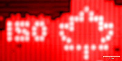
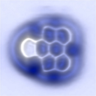
To demonstrate the new discovery, Achal, Wolkow, and their fellow scientists not only fabricated the world’s smallest maple leaf, they also encoded the entire alphabet at a density of 138 terabytes, roughly equivalent to writing 350,000 letters across a grain of rice. For a playful twist, Achal also encoded music as an atom-sized song, the first 24 notes of which will make any video-game player of the 80s and 90s nostalgic for yesteryear but excited for the future of technology and society.

As noted in the news release, there is an atom-sized song, which is available in this video,

As for the nano-sized maple leaf, I highlighted that bit of whimsy in a June 30, 2017 posting.

Here’s a link to and a citation for the paper,

Lithography for robust and editable atomic-scale silicon devices and memories by Roshan Achal, Mohammad Rashidi, Jeremiah Croshaw, David Churchill, Marco Taucer, Taleana Huff, Martin Cloutier, Jason Pitters, & Robert A. Wolkow. Nature Communicationsvolume 9, Article number: 2778 (2018) DOI: https://doi.org/10.1038/s41467-018-05171-y Published 23 July 2018

This paper is open access.

For interested parties, you can find Quantum Silicon (QSI) here. My Edmonton geography is all but nonexistent, still, it seems to me the company address on Saskatchewan Drive is a University of Alberta address. It’s also the address for the National Research Council of Canada. Perhaps this is a university/government spin-off company?

The ‘interview’

I sent some questions to the researchers at the University of Alberta who very kindly provided me with the following answers. Roshan Achal passed on one of the questions to his colleague Taleana Huff for her response. Both Achal and Huff are associated with QSI.

Unfortunately I could not find any pictures of all three researchers (Achal, Huff, and Wolkow) together.

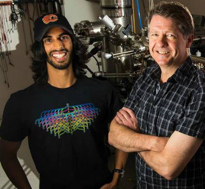
Roshan Achal (left) used nanotechnology perfected by his PhD supervisor, Robert Wolkow (right) to create atomic-scale computer memory that could exceed the capacity of today’s solid-state storage drives by 1,000 times. (Photo: Faculty of Science)

(1) SHRINKING THE MANUFACTURING PROCESS TO THE ATOMIC SCALE HAS
ATTRACTED A LOT OF ATTENTION OVER THE YEARS STARTING WITH SCIENCE
FICTION OR RICHARD FEYNMAN OR K. ERIC DREXLER, ETC. IN ANY EVENT, THE
ORIGINS ARE CONTESTED SO I WON’T PUT YOU ON THE SPOT BY ASKING WHO
STARTED IT ALL INSTEAD ASKING HOW DID YOU GET STARTED?

I got started in this field about 6 years ago, when I undertook a MSc
with Dr. Wolkow here at the University of Alberta. Before that point, I
had only ever heard of a scanning tunneling microscope from what was
taught in my classes. I was aware of the famous IBM logo made up from
just a handful of atoms using this machine, but I didn’t know what
else could be done. Here, Dr. Wolkow introduced me to his line of
research, and I saw the immense potential for growth in this area and
decided to pursue it further. I had the chance to interact with and
learn from nanofabrication experts and gain the skills necessary to
begin playing around with my own techniques and ideas during my PhD.

(2) AS I UNDERSTAND IT, THESE ARE THE PIECES YOU’VE BEEN
WORKING ON: (1) THE TUNGSTEN MICROSCOPE TIP, WHICH MAKE[s] (2) THE SMALLEST
QUANTUM DOTS (SINGLE ATOMS OF SILICON), (3) THE AUTOMATION OF THE
QUANTUM DOT PRODUCTION PROCESS, AND (4) THE “MOST DENSE SOLID-STATE
MEMORY EVER CREATED.” WHAT’S MISSING FROM THE LIST AND IS THAT WHAT
YOU’RE WORKING ON NOW?

One of the things missing from the list, that we are currently working
on, is the ability to easily communicate (electrically) from the
macroscale (our world) to the nanoscale, without the use of a scanning
tunneling microscope. With this, we would be able to then construct
devices using the other pieces we’ve developed up to this point, and
then integrate them with more conventional electronics. This would bring
us yet another step closer to the realization of atomic-scale
electronics.

(3) PERHAPS YOU COULD CLARIFY SOMETHING FOR ME. USUALLY WHEN SOLID STATE
MEMORY IS MENTIONED, THERE’S GREAT CONCERN ABOUT MOORE’S LAW. IS
THIS WORK GOING TO CREATE A NEW LAW? AND, WHAT IF ANYTHING DOES
;YOUR MEMORY DEVICE HAVE TO DO WITH QUANTUM COMPUTING?

That is an interesting question. With the density we’ve achieved,
there are not too many surfaces where atomic sites are more closely
spaced to allow for another factor of two improvement. In that sense, it
would be difficult to improve memory densities further using these
techniques alone. In order to continue Moore’s law, new techniques, or
storage methods would have to be developed to move beyond atomic-scale
storage.

The memory design itself does not have anything to do with quantum
computing, however, the lithographic techniques developed through our
work, may enable the development of certain quantum-dot-based quantum
computing schemes.

(4) THIS MAY BE A LITTLE OUT OF LEFT FIELD (OR FURTHER OUT THAN THE
OTHERS), COULD;YOUR MEMORY DEVICE HAVE AN IMPACT ON THE
DEVELOPMENT OF CRYPTOCURRENCY AND BLOCKCHAIN? IF SO, WHAT MIGHT THAT
IMPACT BE?

I am not very familiar with these topics, however, co-author Taleana
Huff has provided some thoughts:

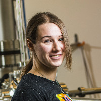
Taleana Huff (downloaded from https://ca.linkedin.com/in/taleana-huff]

“The memory, as we’ve designed it, might not have too much of an
impact in and of itself. Cryptocurrencies fall into two categories.
Proof of Work and Proof of Stake. Proof of Work relies on raw
computational power to solve a difficult math problem. If you solve it,
you get rewarded with a small amount of that coin. The problem is that
it can take a lot of power and energy for your computer to crunch
through that problem. Faster access to memory alone could perhaps
streamline small parts of this slightly, but it would be very slight.
Proof of Stake is already quite power efficient and wouldn’t really
have a drastic advantage from better faster computers.

Now, atomic-scale circuitry built using these new lithographic
techniques that we’ve developed, which could perform computations at
significantly lower energy costs, would be huge for Proof of Work coins.
One of the things holding bitcoin back, for example, is that mining it
is now consuming power on the order of the annual energy consumption
required by small countries. A more efficient way to mine while still
taking the same amount of time to solve the problem would make bitcoin
much more attractive as a currency.”

Thank you to Roshan Achal and Taleana Huff for helping me to further explore the implications of their work with Dr. Wolkow.

Comments

As usual, after receiving the replies I have more questions but these people have other things to do so I’ll content myself with noting that there is something extraordinary in the fact that we can imagine a near future where atomic scale manufacturing is possible and where as Achal says, ” … storage methods would have to be developed to move beyond atomic-scale [emphasis mine] storage”. In decades past it was the stuff of science fiction or of theorists who didn’t have the tools to turn the idea into a reality. With Wolkow’s, Achal’s, Hauff’s, and their colleagues’ work, atomic scale manufacturing is attainable in the foreseeable future.

Hopefully we’ll be wiser than we have been in the past in how we deploy these new manufacturing techniques. Of course, before we need the wisdom, scientists, as  Achal notes,  need to find a new way to communicate between the macroscale and the nanoscale.

As for Huff’s comments about cryptocurrencies and cyptocurrency and blockchain technology, I stumbled across this very recent research, from a July 31, 2018 Elsevier press release (also on EurekAlert),

A study [behind a paywall] published in Energy Research & Social Science warns that failure to lower the energy use by Bitcoin and similar Blockchain designs may prevent nations from reaching their climate change mitigation obligations under the Paris Agreement.

The study, authored by Jon Truby, PhD, Assistant Professor, Director of the Centre for Law & Development, College of Law, Qatar University, Doha, Qatar, evaluates the financial and legal options available to lawmakers to moderate blockchain-related energy consumption and foster a sustainable and innovative technology sector. Based on this rigorous review and analysis of the technologies, ownership models, and jurisdictional case law and practices, the article recommends an approach that imposes new taxes, charges, or restrictions to reduce demand by users, miners, and miner manufacturers who employ polluting technologies, and offers incentives that encourage developers to create less energy-intensive/carbon-neutral Blockchain.

“Digital currency mining is the first major industry developed from Blockchain, because its transactions alone consume more electricity than entire nations,” said Dr. Truby. “It needs to be directed towards sustainability if it is to realize its potential advantages.

“Many developers have taken no account of the environmental impact of their designs, so we must encourage them to adopt consensus protocols that do not result in high emissions. Taking no action means we are subsidizing high energy-consuming technology and causing future Blockchain developers to follow the same harmful path. We need to de-socialize the environmental costs involved while continuing to encourage progress of this important technology to unlock its potential economic, environmental, and social benefits,” explained Dr. Truby.

As a digital ledger that is accessible to, and trusted by all participants, Blockchain technology decentralizes and transforms the exchange of assets through peer-to-peer verification and payments. Blockchain technology has been advocated as being capable of delivering environmental and social benefits under the UN’s Sustainable Development Goals. However, Bitcoin’s system has been built in a way that is reminiscent of physical mining of natural resources – costs and efforts rise as the system reaches the ultimate resource limit and the mining of new resources requires increasing hardware resources, which consume huge amounts of electricity.

Putting this into perspective, Dr. Truby said, “the processes involved in a single Bitcoin transaction could provide electricity to a British home for a month – with the environmental costs socialized for private benefit.

“Bitcoin is here to stay, and so, future models must be designed without reliance on energy consumption so disproportionate on their economic or social benefits.”

The study evaluates various Blockchain technologies by their carbon footprints and recommends how to tax or restrict Blockchain types at different phases of production and use to discourage polluting versions and encourage cleaner alternatives. It also analyzes the legal measures that can be introduced to encourage technology innovators to develop low-emissions Blockchain designs. The specific recommendations include imposing levies to prevent path-dependent inertia from constraining innovation:

  • Registration fees collected by brokers from digital coin buyers.
  • “Bitcoin Sin Tax” surcharge on digital currency ownership.
  • Green taxes and restrictions on machinery purchases/imports (e.g. Bitcoin mining machines).
  • Smart contract transaction charges.

According to Dr. Truby, these findings may lead to new taxes, charges or restrictions, but could also lead to financial rewards for innovators developing carbon-neutral Blockchain.

The press release doesn’t fully reflect Dr. Truby’s thoughtfulness or the incentives he has suggested. it’s not all surcharges, taxes, and fees constitute encouragement.  Here’s a sample from the conclusion,

The possibilities of Blockchain are endless and incentivisation can help solve various climate change issues, such as through the development of digital currencies to fund climate finance programmes. This type of public-private finance initiative is envisioned in the Paris Agreement, and fiscal tools can incentivize innovators to design financially rewarding Blockchain technology that also achieves environmental goals. Bitcoin, for example, has various utilitarian intentions in its White Paper, which may or may not turn out to be as envisioned, but it would not have been such a success without investors seeking remarkable returns. Embracing such technology, and promoting a shift in behaviour with such fiscal tools, can turn the industry itself towards achieving innovative solutions for environmental goals.

I realize Wolkow, et. al, are not focused on cryptocurrency and blockchain technology per se but as Huff notes in her reply, “… new lithographic techniques that we’ve developed, which could perform computations at significantly lower energy costs, would be huge for Proof of Work coins.”

Whether or not there are implications for cryptocurrencies, energy needs, climate change, etc., it’s the kind of innovative work being done by scientists at the University of Alberta which may have implications in fields far beyond the researchers’ original intentions such as more efficient computation and data storage.

ETA Aug. 6, 2018: Dexter Johnson weighed in with an August 3, 2018 posting on his Nanoclast blog (on the IEEE [Institute of Electrical and Electronics Engineers] website),

Researchers at the University of Alberta in Canada have developed a new approach to rewritable data storage technology by using a scanning tunneling microscope (STM) to remove and replace hydrogen atoms from the surface of a silicon wafer. If this approach realizes its potential, it could lead to a data storage technology capable of storing 1,000 times more data than today’s hard drives, up to 138 terabytes per square inch.

As a bit of background, Gerd Binnig and Heinrich Rohrer developed the first STM in 1986 for which they later received the Nobel Prize in physics. In the over 30 years since an STM first imaged an atom by exploiting a phenomenon known as tunneling—which causes electrons to jump from the surface atoms of a material to the tip of an ultrasharp electrode suspended a few angstroms above—the technology has become the backbone of so-called nanotechnology.

In addition to imaging the world on the atomic scale for the last thirty years, STMs have been experimented with as a potential data storage device. Last year, we reported on how IBM (where Binnig and Rohrer first developed the STM) used an STM in combination with an iron atom to serve as an electron-spin resonance sensor to read the magnetic pole of holmium atoms. The north and south poles of the holmium atoms served as the 0 and 1 of digital logic.

The Canadian researchers have taken a somewhat different approach to making an STM into a data storage device by automating a known technique that uses the ultrasharp tip of the STM to apply a voltage pulse above an atom to remove individual hydrogen atoms from the surface of a silicon wafer. Once the atom has been removed, there is a vacancy on the surface. These vacancies can be patterned on the surface to create devices and memories.

If you have the time, I recommend reading Dexter’s posting as he provides clear explanations, additional insight into the work, and more historical detail.

Canada: Happy 150th anniversary!

There’s a bit of fun in the title for Jennifer Pascoe’s June 27, 2017 University of Alberta news release, (assuming you’re familiar with the opening words for Canada’s national anthem: “O Canada!”),

Nan-Oh-Canada

At just 32 atoms and visible only through a million-dollar scanning tunneling microscope, a tiny maple leaf created by UAlberta PhD student Roshan Achal illustrates the next wave of green technology, all while showing patriotic pride.

Invisible to the naked eye, the little leaf is pulling triple duty: celebrating Canada’s 150th birthday, attempting a world record, and—with critical implications for our technology-driven information society—providing critical steps towards the next generation of smaller and faster computers.

“It’s super cool and super Canadian and demonstrates our strength and skill in this niche of nanotechnology,” said Achal. “Almost no one else in the world can do it this well.”

Unlike other ultra-small atomic creations, this maple leaf retains its structure at room temperature.

A tiny act of patriotism

At ten nanometres in width, the leaf is roughly 100 times smaller than the world’s smallest national flag—created at the University of Waterloo in September 2016—10,000 times smaller than a human hair, and 53 million times smaller than the world’s largest maple leaf.

The leaf demonstrates the technique of building structures atom by atom (via something called scanning tunneling microscopy), which is being used to create and study circuitry to make smaller computational components while simultaneously speeding them up. In this particular niche of nanotechnology, Canada rates high on the international stage, with the University of Alberta leading the way.

“It’s hard to imagine, because it’s so small, but picture a surface almost like bubble wrap,” explained Achal of the silicon crystal wafer on which the leaf is patterned. “The bubbles are actually hydrogen atoms bonded to the surface, and we are able to pop those bubbles to create patterns.”

Nano pioneers

Achal is working on perfecting that patterning process to make atomic structures which will help revolutionize the next generation of computing by consuming less power. He’s using an ultra-sharp tool, a tip just one atom in width, which was perfected by his supervisor, UAlberta physics professor Robert Wolkow, whom Achal calls a “visionary.”

A pioneer in scanning tunneling microscopy technology, Wolkow already has a Guinness World Record for the nano-tip, the world’s sharpest man-made object, which provides unparalleled precision for patterning electronic circuits.

Achal explained the team wanted to do something to demonstrate their technological capabilities, but also something fun and meaningful to mark the occasion of Canada 150.

While they wait to hear back from Guinness World Records with an official nod to their small sculpture, the scientists continue to perfect their technique, with significant implications for next generation computing. This capability is now being put to commercial use by local spin-off Quantum Silicon Incorporated to make revolutionary ultra-fast and efficient silicon electronic devices.

It’s nice to see the enthusiasm although calling Wolkow ‘a visionary’ seems a little over the top especially with all of the other exuberance (super Canadian?). In any event, there are very few visionaries, maybe Wolkow could have been described as amazing, groundbreaking, and/or extraordinary?

Getting back to the point: Happy 150th Canada Day July 1, 2017!

h/t June 27, 2017 news item on Nanowerk.

Molecules (arynes) seen for first time in 113 years

Arynes were first theorized in 1902 and they’ve been used as building blocks to synthesize a variety of compounds but they’re existence hasn’t been confirmed until now.

AFM image of an aryne molecule imaged with a CO tip. Courtesy: IBM

AFM image of an aryne molecule imaged with a CO tip. Courtesy: IBM

A July 13, 2015 news item in Nanowerk makes the announcement (Note: A link has been removed),

chemistry teachers and students can breath a sigh of relief. After teaching and learning about a particular family of molecules for decades, scientists have finally proven that they do in fact exist.

In a new paper published online today in Nature Chemistry (“On-surface generation and imaging of arynes by atomic force microscopy”), scientists from IBM Research and CIQUS at the University of Santiago de Compostela, Spain, have confirmed the existence and characterized the structure of arynes, a family of highly-reactive short-lived molecules which was first suggested 113 years ago. The technique has broad applications for on-surface chemistry and electronics, including the preparation of graphene nanoribbons and novel single-molecule devices.

A July 13, 2015 IBM news release by Chris Sciacca, which originated the news item, describes arynes and the imaging process used to capture them for the first time (Note: Links have been removed),

“Arynes are discussed in almost every undergraduate course on organic chemistry around the world. Therefore, it’s kind of a relief to find the final confirmation that these molecules truly exist,” said Prof. Diego Peña, a chemist at the University of Santiago de Compostela.

“I look forward to seeing new chemical challenges solved by the combination of organic synthesis and atomic force microscopy.”

There are trillions of molecules in the universe and some of them are stable enough to be isolated and characterized, but many others are so short-lived that they can only be proposed indirectly, via chemical reactions or spectroscopic methods.

One such species are arynes, which were first suggested in 1902, and since then have been used as intermediates or building blocks in the synthesis of a variety of compounds for applications including medicine, organic electronics and molecular materials. The challenge with these particular molecules is that they only exist for several milliseconds making them extremely challenging to image, until now.

The imaging was accomplished by means of atomic force microscopy (AFM), a scanning technique that can accomplish nanometer-level resolution. After the preparation of the key aryne precursor by CIQUS, IBM scientists used the sharp tip of a scanning tunneling microscope (STM) to generate individual aryne molecules from precursor molecules by atomic manipulation. The experiments were performed on films of sodium chloride, at temperatures near absolute zero, to stabilize the aryne.

Once the molecules were isolated, the team used AFM to measure the tiny forces between the STM tip, which is terminated with a single carbon monoxide molecule, and the sample to image the aryne’s molecular structure. The resulting image was so clear that the scientists could study their chemical nature based on the minute differences between individual bonds.

“Our team has developed several state-of-the-art techniques since 2009, which made this achievement possible,” said Dr. Niko Pavliček, a physicist at IBM Research – Zurich and lead author of the paper. “For this study, it was absolutely essential to pick an insulating film on which the molecules were adsorbed and to deliberately choose the atomic tip-terminations to probe them. We hope this technique will have profound effects on the future of chemistry and electronics.”

Prof. Peña, added that “These findings on arynes can be compared with the long-standing search for the giant squid. For centuries, fishermen had found clues of the existence of this legendary animal. But it was only very recently that scientists managed to film a giant squid alive. In both cases, state-of-the-art technologies were crucial to observe these elusive species alive: a low-noise submarine for the giant squid; a low-temperature AFM for the aryne.”

This research is part of IBM’s five-year, $3 billion investment to push the limits of chip technology and semiconductor innovations needed to meet the emerging demands of cloud computing and Big Data systems.

This work is a result of the large European project called (Planar Atomic and Molecular Scale Devices). PAMS’ main objective is to develop and investigate novel electronic devices of nanometric-scale size. Part of this research is also funded by a European Research Council Advanced Grant awarded to IBM scientist Gerhard Meyer, who is also a co-author of the paper.

Here’s a link to and a citation for the paper,

On-surface generation and imaging of arynes by atomic force microscopy by Niko Pavliček, Bruno Schuler, Sara Collazos, Nikolaj Moll, Dolores Pérez, Enrique Guitián, Gerhard Meyer, Diego Peña, & Leo Gross. Nature Chemistry (2015) doi:10.1038/nchem.2300 Published online 13 July 2015

This paper is behind a paywall.

Alberta’s summer of 2014 nano funding and the US nano community’s talks with the House of Representatives

I have two items concerning nanotechnology and funding. The first item features Michelle Rempel, Canada’s Minister of State for Western Economic Diversification (WD) who made two funding announcements this summer (2014) affecting the Canadian nanotechnology sector and, more specifically, the province of Alberta.

A June 20, 2014 WD Canada news release announced a $1.1M award to the University of Alberta,

Today, the Honourable Michelle Rempel, Minister of State for Western Economic Diversification, announced $1.1 million to help advance leading-edge atomic computing technologies.

Federal funds will support the University of Alberta with the purchase of an ultra-high resolution scanning tunneling microscope, which will enable researchers and scientists in western Canada and abroad to analyze electron dynamics and nanostructures at an atomic level. The first of its kind in North America, the microscope has the potential to significantly transform the semiconductor industry, as research findings aid in the prototype development and technology commercialization of new ultra low-power and low-temperature computing devices and industrial applications.

This initiative is expected to further strengthen Canada’s competitive position throughout the electronics value chain, such as microelectronics, information and communications technology, and the aerospace and defence sectors. The project will also equip graduate students with a solid foundation of knowledge and hands-on experience to become highly qualified, skilled individuals in today’s workforce.

One month later, a July 21, 2014 WD news release (hosted on the Alberta Centre for Advanced Micro and Nano Products [ACAMP]) announces this award,

Today, the Honourable Michelle Rempel, Minister of State for Western Economic Diversification, announced an investment of $3.3 million toward the purchase and installation of specialized advanced manufacturing and product development equipment at the Alberta Centre for Advanced Micro Nano Technology Products (ACAMP), as well as training on the use of this new equipment for small- and medium-sized enterprises (SMEs).

This support, combined with an investment of $800,000 from Alberta Innovates Technology Futures, will enable ACAMP to expand their services and provide businesses with affordable access to prototype manufacturing that is currently unavailable in western Canada. By helping SMEs accelerate the development and commercialization of innovative products, this project will help strengthen the global competitiveness of western Canadian technology companies.

Approximately 80 Alberta SMEs will benefit from this initiative, which is expected to result in the development of new product prototypes, the creation of new jobs in the field, as well as connections between SMEs and multi-national companies. This equipment will also assist ACAMP’s outreach activities across the western Canadian provinces.

I’m not entirely clear as to whether or not the June 2014 $1.1M award is considered part of the $3.3M award or if these are two different announcements. I am still waiting for answers to a June 20, 2014 query sent to Emily Goucher, Director of Communications to the Hon. Michelle Rempel,

Hi Emily!

Thank you for both the news release and the information about the embargo … happily not an issue at this point …

I noticed Robert Wolkow’s name in the release (I last posted about his work in a March 3, 2011 piece about his and his team’s entry into the Guinness Book of Records for the world’s smallest electron microscope tip (http://www.frogheart.ca/?tag=robert-wolkow) [Note: Wolkow was included in a list of quotees not included here in this July 29, 2014 posting]

I am assuming that the new microscope at the University of Alberta is specific to a different type of work than the one at UVic, which has a subatomic microscope (http://www.frogheart.ca/?p=10426)

Do I understand correctly that an STM is being purchased or is this an announcement of the funds and their intended use with no details about the STM available yet? After reading the news release closely, it looks to me like they do have a specific STM in mind but perhaps they don’t feel ready to make a purchase announcement yet?

If there is information about the STM that will be purchased I would deeply appreciate receiving it.

Thank you for your time.

As I wait, there’s more news from  the US as members of that country’s nanotechnology community testify at a second hearing before the House of Representatives. The first (a May 20, 2014 ‘National Nanotechnology Initiative’ hearing held before the Science, Space, and Technology
Subcommittee on Research and Technology) was mentioned in an May 23, 2014 posting  where I speculated about the community’s response to a smaller budget allocation (down to $1.5B in 2015 from $1.7B in 2014).

This second hearing is being held before the Energy and Commerce Subcommittee on Commerce, Manufacturing and Trade and features an appearance by James Tour from Rice University according to a July 28, 2014 news item on Azonano,

At the hearing, titled “Nanotechnology: Understanding How Small Solutions Drive Big Innovation,” Tour will discuss and provide written testimony on the future of nanotechnology and its impact on U.S. manufacturing and jobs. Tour is one of the most cited chemists in the country, and his Tour Group is a leader in patenting and bringing to market nanotechnology-based methods and materials.

Who: James Tour, Rice’s T.T. and W.F. Chao Chair in Chemistry and professor of materials science and nanoengineering and of computer science.

What: Exploring breakthrough nanotechnology opportunities.

When: 10:15 a.m. EDT Tuesday, July 29.

Where: Room 2322, Rayburn House Office Building, Washington, D.C.

The hearing will explore the current state of nanotechnology and the direction it is headed so that members can gain a better understanding of the policy changes that may be necessary to keep up with advancements. Ultimately, the subcommittee hopes to better understand what issues will confront regulators and how to assess the challenges and opportunities of nanotechnology.

You can find a notice for this July 2014 hearing and a list of witnesses along with their statements here. As for what a second hearing might mean within the context of the US National Nanotechnology Initiative, I cannot say with any certainty. But, this is the first time in six years of writing this blog where there have been two hearings post-budget but as a passive collector of this kind of information this may be a reflection of my information collection strategies rather than a response to a smaller budget allocation. Still, it’s interesting.

R.I.P. Heinrich Rohrer, co-inventor of the scanning tunneling microscope, 1933-2013

Heinrich Rohrer died May 16, 2013 according to the May 22, 2013 news item on Nanowerk,

The co-inventor of the scanning tunneling microscope, Dr. Heinrich Rohrer, passed away on the evening of May 16, 2013. He was 79.

Heinrich Rohrer, IBM Fellow and Nobel Laureate, joined the IBM Research Laboratory in Zurich, Switzerland, in December of 1963, where he worked for 34 years.

After hiring a young scientist named Gerd Binnig in the late 1970s, the two started collaborating, brought closely together by their backgrounds in superconductivity and their fascination with atomic surfaces. The two scientists grew increasingly frustrated by the limits of the tools then available to study the distinct characteristics of atomic surfaces, so they decided to build their own, something that would be capable of seeing and manipulating atoms at the nanoscale level.

The May 2013 obituary on the IBM research website, which originated the news item, commemorates Rohrer’s Nobel winning accomplishment, the co-invention of the scanning tunneling microscope (STM),

Dr. Heinrich Rohrer, IBM Fellow, Nobel Laureate and co-inventor of the scanning tunneling microscope, passed away on the evening of May 16, 2013. He was 79. Dr. Rohrer joined IBM Research – Zurich in December of 1963, where he worked for 34 years.

“The invention of the scanning tunneling microscope was a seminal moment in the history of science and information technology,” said Dr. John E. Kelly III, IBM senior vice president and director of Research. “This invention gave scientists the ability to image, measure and manipulate atoms for the first time, and opened new avenues for information technology that we are still pursuing today.”

After hiring a young scientist named Gerd Binnig in the late 1970s, the two started collaborating, brought together by their backgrounds in superconductivity and their fascination with atomic surfaces. They grew increasingly frustrated by the limits of the tools then available, so they built their own, capable of seeing and manipulating atoms at the nanoscale level.

They began experimenting with tunneling, a quantum phenomenon in which electrons can escape the surface of a solid. When another surface approaches, the electron clouds can overlap and an electric current can flow.

Binnig and Rohrer found that when maneuvering a sharp metal conducting tip over the surface of a sample, the amount of electrical current flowing between the tip and the surface could be measured. Variations in the current provided information about the inner structure, and from this information,  they could build a three-dimensional atomic-scale map of the sample’s surface.

In January 1979, Binnig and Rohrer submitted their first patent disclosure on the scanning tunneling microscope (STM). Soon afterwards, with the help of fellow IBM researcher Christoph Gerber, they began to design and construct the microscope.

In awarding Binnig and Rohrer the Nobel Prize in Physics in 1986, just five years after the first STM had been built, the Nobel committee said the invention opened up “entirely new fields… for the study of the structure of matter.”

In 2011, in the presence of 600 guests from throughout the research community, IBM and ETH Zurich dedicated the Binnig and Rohrer Nanotechnology Center in Rüschlikon in honor of the scientists’ achievements.

“ For me, Heini was father figure, role model, emotional and spiritual teacher, and best friend – all rolled into one. An eminent person, with an incredible sense of humanity and kindness. ”

-Gerd Binnig

Heinrich Rohrer was as famous for his kindly personality as for his sharp wit and humor. During the opening ceremony of the Center he participated in a public discussion with Binnig and Dr. Ralph Eicher, then president of ETH Zurich. After Binnig attempted to explain their invention, Rohrer jokingly apologized to the audience saying, “If you didn’t quite understand what Gerd just told you, you are not alone.”

Here are a few biographical details from the obituary page on the IBM website,

Heinrich Rohrer was born on June 6, 1933, in Buchs, Switzerland. In 1949, the Rohrer family moved to Zurich and a few years later Heinrich enrolled at the Swiss Federal Institute of Technology in Zurich (ETH), where he studied Physics under Wolfgang Pauli.

In the summer of 1961, Heinrich married Rose-Marie Egger and their honeymoon in the United States led to a two-year project studying thermal conductivity of type-II superconductors and metals at Rutgers University. Shortly thereafter in 1963, he returned to Switzerland to join the Physics department at the newly founded IBM Research – Zurich Laboratory.

The rest, as they say, is history.

ETA May 23, 2013: Dexter Johnson wrote a touching tribute in his May 23, 2013 posting, Heinrich Rohrer: The Modest Pioneer of Nanotechnology.

MORPHONANO, an art/sci exhibit in California

This description of the event (MORPHONANO) which is being held at the Beall Center at the University of California (Irvine) comes from the Beall Center’s home page,

MORPHONANO explores a number of art works created by media artist Victoria Vesna and nanoscientist James Gimzewski. Their collaborative works create an intersection of space, time and embodiment by employing a very subtle and responsive energetic exchange. Participants interact with the works in mindful ways resulting in rich visual and sonic experiences within a meditative space. By reversing the scale of nanotechnology to the realm of human experience, the artist and scientist create a sublime reversal of space-time.

Here’s an image depicting one of the exhibits in the show,

ZERO@WAVEFUNCTION plays with the idea of scale and molecular manipulation from a distance with the participant changing the structures of the buckyballs with their shadows, a real time interactive metaphor of the scanning tunneling microscope (STM).

It looks to me that the idea is to ’embody’ the nanoscale as per the caption “the participants changing the structures of the buckyballs with their shadows, a real time interactive metaphor of the scanning tunneling microscope.” There’s a larger version of the image and information about this exhibit in the Feb. 14, 2012 news item on Nanowerk,

BLUE MORPH is an interactive installation that uses nanoscale images combined with sounds derived from the microscopic undulations of a chrysalis during the period of its metamorphosis into a butterfly recorded using nanotechnology. The work is designed to be responsive to minute, subtle, mindful movements of the participant creating a rich visual and sonic experience of morphing. Most is revealed in complete stillness.

NANOMANDALA is a video projected onto a disk of sand, 8 feet in diameter. Visitors can touch the sand as images are projected in evolving scale from the molecular structure of a single grain of sand – achieved my means of photography, optical and scanning electron microscopy (SEM) – to the recognizable image of the complete mandala, and then back again. The original Chakrasamvara mandala was created by monks of the Ghaden Lhopa Khangsten monastery. Patience will allow experiencing the whole.

ZERO@WAVEFUNCTION plays with the idea of scale and molecular manipulation from a distance with the participant changing the structures of the buckyballs with their shadows, a real time interactive metaphor of the scanning tunneling microscope (STM). Slow motion makes change happen.

BRAIN STORMING: SOUNDS OF THINKING a premier of a work of self organization in progress focusing on scale invariant and the brain using biometric data. A number of brain storming sessions with cutting neuroscientists, nanotechnologists, philosophers and monks will take place throughout the exhibition. In many ways the works in this exhibition reverse the scale of nanotechnology to a visible realm and time in nano scale creating a sublime reversal of space-time.

The show opened Feb. 2 and closes May 6, 2012. The address is

Beall Center for Art + Technology
University of California, Irvine
Claire Trevor School of the Arts
712 Arts Plaza
Irvine, CA 92697-2775
www.beallcenter.uci.edu

Here are some details about the art/sci collaborators, Victoria Vesna and James Gimzewski, from the undated Beall Center news release,

Victoria Vesna is a media artist and Professor at the Department of Design | Media Arts at the UCLA School of the Arts and director of the UCLA Art|Sci center. Currently she is Visiting Professor at Art, Media + Technology, Parsons the New School for Design in New York and a senior researcher at IMéRA – Institut Méditerranéen de Recherches Avancées in Marseille, France. Her work can be defined as experimental creative research that resides between disciplines and technologies. She explores how communication technologies affect collective behavior and how perceptions of identity shift in relation to scientific innovation. Her most recent experiential installations — Blue Morph, Water Bowls, Hox Zodiac, all aim to raise consciousness around environmental issues natural and human-animal relations. …

James Gimzewski FRS is a distinguished Professor in the Dept. of Chemistry and Biochemistry at UCLA. He is director of Pico and Nano core laboratory at the California NanoSynstems Institute (CNSI). He is also scientific director of the Art | Sci center and a senior fellow of IMéRA. He is a satellite co-director and PI of materials nanoarchitectonics at the National Institute of Material Science in Tsukuba, Japan. Until February 2001, he was a group leader at the IBM Zurich Labs, where he was involved in Nanoscale science since 1983. He pioneered research on electrical contact with single atoms and molecules, light emission and molecular imaging using STM. His accomplishments include the first STM-manipulation of molecules at room temperature, the realization of molecular abacus using buckyballs, the discovery of single molecule rotors and the development of nanomechanical sensors based on nanotechnology, which explore the ultimate limits of sensitivity and measurement. …

I have mentioned Gimzewski previously in a post (Oct. 17, 2011) about a three-part nanotechnology series on Canadian television.

Canada’s National Science and Technology Week 2011

October 14 – 23, 2011 has been designated as Canada’s National Science and Technology ‘week‘. From the October 7, 2011 newsletter from the Canada Science and Technology Museums Corporation,

We are proud to provide national coordination for Canada’s National Science and Technology Week (NSTW). Launch ceremony will coincide with the opening of CBC ]Canadian Broadcasting Corporation]-Radio Canada exhibition. Locally, our museums will mark the week with lots of lectures, events, demonstrations and exhibitions.

Here’s a video of Dr. Rashmi Venkateswaran from the University of Ottawa promoting National Science and Technology Week and talking about why she believes understanding science is so important for everyone,

There’s a listing of this year’s events across the country, here. I notice that in the province of British Columbia (where I’m located), there are a total of 11 listed, most of them in Vancouver or Victoria. Here are a few that caught my attention,

Girl Guides

Name of Event: All about Science
Location: Chilliwack, BC
Date of Event: Oct 18 2011
Event Details: We are going to do some science experiments, talk about Canadian inventors, and do activities from the Activity Book 3.

British Columbia Innovation Council [BCIC]

Name of Event: BCIC’s Innovation Exploration
Location: Victoria, BC
Date: October 24th and 25th 2011
Event Details: Closed event: Established in 1990, BCIC’s Innovation Exploration program recognizes British Columbia and the Yukon’s leading secondary students who represent their regions at the Canada-Wide Science Fair. The program provides top students with an opportunity to explore post-secondary education and career opportunities available to them in science and technology in BC. This year, for the first time ever, BCIC is hosting the Innovation Exploration program in Victoria, and will welcome 66 accomplished students for two days of activities and meetings with members of Victoria’s tech community including the Victoria Advanced Technology Council (VIATeC), Vancouver Island Technology Park (VITP), Centre of the Universe (Astronomy Interpretive Centre), the University of Victoria (UVic), and the Institute for Ocean Sciences (IOS). The event will culminate at the Opening Dinner held at Royal BC Museum with members of government, industry and academia in attendance and a keynote presentation delivered by Astronomer Dr. Doug Johnstone.

TRIUMF

Name of Event: TRIUMF Saturday Morning Lectures
Location: TRIUMF Auditorium [University of British Columbia]
Date of Event: October 15, 2011
Event Details: TRIUMF, UBC, and SFU present a series of lectures on the frontiers of modern physics at a level suitable for high school students or the general public. This lecture will cover “The Future of Nuclear Medicine” by TRIUMF scientist Dr. Paul Schaffer, and “Scanning Tunnelling Microscopy: In Touch with Atoms” by Dr. Yan Pennec of UBC.

Vancouver Women’s Club and SCWIST – Society for Canadian Women in Science and Technology

Name of Event: Climbing the Ladder
Location: Hycroft University Women’s Club of Vancouver 1489 McRae Avenue, Vancouver, BC
Date of Event: October 20, 2011
Event Details: Networking event hosted by the Vancouver Women’s Club and SCWIST – Society for Canadian Women in Science and Technology- promoting women in science, technology and management positions. Panel discussion with the following renowned individuals:
Anne Naser — Chief Information Officer (CIO)
Pamela Cohen — Vice President — Human Resources & Facilities
Joo Choon — Manager — Systems Development & Support
Andrea Goddard — Manager — HR Operations & IT Specialist
Izabella Wieckowski — Manager — IT Solutions
Zorana (Ana) Ostojic – Senior Engineer

$20 – non members free – SCWIST members (become a member today!)

Richmond Public Library

Name of Event: 5th Annual Brighouse Science Celebration
Location: Main branch of the Richmond Public Library
Date of Event: Friday, October 21st, 2011
Event Details: Join us October 21st (10:00 – 4:00) in celebrating the diverse sciences used in the classroom and workplace here in B.C. Building upon the huge success of previous years we hope to make this Pro-D event the biggest of them all by hosting the largest number of government and non-government groups. Bring your children for some hands-on science fun!

The Canada Science and Technology Museums Corporation lists these events for their celebration of Canada’s National Science and Technology Week. Unfortunately, I could not find any additional information about the CBC-Radio Canada 75th Anniversary exhibition on the museum website.

Scientific research, failure, and the scanning tunneling microscope

“99% of all you do is failure and that’s maybe the most difficult part of basic research,” said Gerd Binnig in a snippet I’ve culled from an interview with Dexter Johnson (Nanoclast blog on the IEEE [Institute of Electrical and Electronics Engineers] website) posted May 23, 2011 where Binnig discussed why he continued with a project that had failed time and time again. (The snippet is from the 2nd audio file from the top of the posting)

Binnig along with Heinrich Rohrer is a Nobel Laureate. Both men won their award for work on the scanning tunneling microscope (STM), which was the project that had failed countless times and that went on to play an important part in the nanotechnology narrative. Earlier this month, both men were honoured when IBM and ETH Zurich opened the Binnig and Rohrer Nanotechnology Center in Zurich. From the May 17, 2011 news item on Nanowerk,

IBM and ETH Zurich, a premiere European science and engineering university, hosted more than 600 guests from industry, academia and government, to open the Binnig and Rohrer Nanotechnology Center located on the campus of IBM Research – Zurich. The facility is the centerpiece of a 10-year strategic partnership in nanoscience between IBM and ETH Zurich where scientists will research novel nanoscale structures and devices to advance energy and information technologies.

The new Center is named for Gerd Binnig and Heinrich Rohrer, the two IBM scientists and Nobel Laureates who invented the scanning tunneling microscope at the Zurich Research Lab in 1981, thus enabling researchers to see atoms on a surface for the first time. The two scientists attended today’s opening ceremony, at which the new lab was unveiled to the public.

Here’s an excerpt from Dexter’s posting where he gives some context for the audio files,

As promised last week, I would like to share some audio recordings I made of Gerd Binnig and Heinrich Rohrer taking questions from the press during the opening of the new IBM and ETH Zurich nanotechnology laboratory named in their honor.

This first audio file features both Binnig’s and Rohrer’s response to my question of why they were interested in looking at inhomogenities on surfaces in the first place, which led them eventually to creating an instrument for doing it. A more complete history of the STM’s genesis can be found in their joint Nobel lecture here.

The sound quality isn’t the best but these snippets are definitely worth listening to if you find the process of scientific inquiry interesting.

For anyone who’s not familiar with the scanning tunneling microscope, I found this description in the book, Soft Machines; Nanotechnology and Life, by Richard Jones.

Scanning probe microscopes rely on an entirely different principle to both light microscopes and electron microscopes, or indeed our own eyes. Rather than detecting waves that have been scattered from the object we are looking at, on feels the surface of that object with a physical probe. This probe is moved across the surface with high precision. As it tracks the contours of the surface, it s moved up or down in a way that is controlled by some interaction between the tip of the probe and the surface. This interaction could be the flow of electrical current, in the case of a scanning tunneling microscope, or simple the force between the tip and the surface in the case of an atomic force microscope. pp. 17-18