Tag Archives: DARPA

Bringing memristors to the masses and cutting down on energy use

One of my earliest posts featuring memristors (May 9, 2008) focused on their potential for energy savings but since then most of my postings feature research into their application in the field of neuromorphic (brainlike) computing. (For a description and abbreviated history of the memristor go to this page on my Nanotech Mysteries Wiki.)

In a sense this July 30, 2018 news item on Nanowerk is a return to the beginning,

A new way of arranging advanced computer components called memristors on a chip could enable them to be used for general computing, which could cut energy consumption by a factor of 100.

This would improve performance in low power environments such as smartphones or make for more efficient supercomputers, says a University of Michigan researcher.

“Historically, the semiconductor industry has improved performance by making devices faster. But although the processors and memories are very fast, they can’t be efficient because they have to wait for data to come in and out,” said Wei Lu, U-M professor of electrical and computer engineering and co-founder of memristor startup Crossbar Inc.

Memristors might be the answer. Named as a portmanteau of memory and resistor, they can be programmed to have different resistance states–meaning they store information as resistance levels. These circuit elements enable memory and processing in the same device, cutting out the data transfer bottleneck experienced by conventional computers in which the memory is separate from the processor.

A July 30, 2018 University of Michigan news release (also on EurekAlert), which originated the news item, expands on the theme,

… unlike ordinary bits, which are 1 or 0, memristors can have resistances that are on a continuum. Some applications, such as computing that mimics the brain (neuromorphic), take advantage of the analog nature of memristors. But for ordinary computing, trying to differentiate among small variations in the current passing through a memristor device is not precise enough for numerical calculations.

Lu and his colleagues got around this problem by digitizing the current outputs—defining current ranges as specific bit values (i.e., 0 or 1). The team was also able to map large mathematical problems into smaller blocks within the array, improving the efficiency and flexibility of the system.

Computers with these new blocks, which the researchers call “memory-processing units,” could be particularly useful for implementing machine learning and artificial intelligence algorithms. They are also well suited to tasks that are based on matrix operations, such as simulations used for weather prediction. The simplest mathematical matrices, akin to tables with rows and columns of numbers, can map directly onto the grid of memristors.

The memristor array situated on a circuit board.

The memristor array situated on a circuit board. Credit: Mohammed Zidan, Nanoelectronics group, University of Michigan.

Once the memristors are set to represent the numbers, operations that multiply and sum the rows and columns can be taken care of simultaneously, with a set of voltage pulses along the rows. The current measured at the end of each column contains the answers. A typical processor, in contrast, would have to read the value from each cell of the matrix, perform multiplication, and then sum up each column in series.

“We get the multiplication and addition in one step. It’s taken care of through physical laws. We don’t need to manually multiply and sum in a processor,” Lu said.

His team chose to solve partial differential equations as a test for a 32×32 memristor array—which Lu imagines as just one block of a future system. These equations, including those behind weather forecasting, underpin many problems science and engineering but are very challenging to solve. The difficulty comes from the complicated forms and multiple variables needed to model physical phenomena.

When solving partial differential equations exactly is impossible, solving them approximately can require supercomputers. These problems often involve very large matrices of data, so the memory-processor communication bottleneck is neatly solved with a memristor array. The equations Lu’s team used in their demonstration simulated a plasma reactor, such as those used for integrated circuit fabrication.

This work is described in a study, “A general memristor-based partial differential equation solver,” published in the journal Nature Electronics.

It was supported by the Defense Advanced Research Projects Agency (DARPA) (grant no. HR0011-17-2-0018) and by the National Science Foundation (NSF) (grant no. CCF-1617315).

Here’s a link and a citation for the paper,

A general memristor-based partial differential equation solver by Mohammed A. Zidan, YeonJoo Jeong, Jihang Lee, Bing Chen, Shuo Huang, Mark J. Kushner & Wei D. Lu. Nature Electronicsvolume 1, pages411–420 (2018) DOI: https://doi.org/10.1038/s41928-018-0100-6 Published: 13 July 2018

This paper is behind a paywall.

For the curious, Dr. Lu’s startup company, Crossbar can be found here.

7nm (nanometre) chip shakeup

From time to time I check out the latest on attempts to shrink computer chips. In my July 11, 2014 posting I noted IBM’s announcement about developing a 7nm computer chip and later in my July 15, 2015 posting I noted IBM’s announcement of a working 7nm chip (from a July 9, 2015 IBM news release , “The breakthrough, accomplished in partnership with GLOBALFOUNDRIES and Samsung at SUNY Polytechnic Institute’s Colleges of Nanoscale Science and Engineering (SUNY Poly CNSE), could result in the ability to place more than 20 billion tiny switches — transistors — on the fingernail-sized chips that power everything from smartphones to spacecraft.”

I’m not sure what happened to the IBM/Global Foundries/Samsung partnership but Global Foundries recently announced that it will no longer be working on 7nm chips. From an August 27, 2018 Global Foundries news release,

GLOBALFOUNDRIES [GF] today announced an important step in its transformation, continuing the trajectory launched with the appointment of Tom Caulfield as CEO earlier this year. In line with the strategic direction Caulfield has articulated, GF is reshaping its technology portfolio to intensify its focus on delivering truly differentiated offerings for clients in high-growth markets.

GF is realigning its leading-edge FinFET roadmap to serve the next wave of clients that will adopt the technology in the coming years. The company will shift development resources to make its 14/12nm FinFET platform more relevant to these clients, delivering a range of innovative IP and features including RF, embedded memory, low power and more. To support this transition, GF is putting its 7nm FinFET program on hold indefinitely [emphasis mine] and restructuring its research and development teams to support its enhanced portfolio initiatives. This will require a workforce reduction, however a significant number of top technologists will be redeployed on 14/12nm FinFET derivatives and other differentiated offerings.

I tried to find a definition for FinFet but the reference to a MOSFET and in-gate transistors was too much incomprehensible information packed into a tight space, see the FinFET Wikipedia entry for more, if you dare.

Getting back to the 7nm chip issue, Samuel K. Moore (I don’t think he’s related to the Moore of Moore’s law) wrote an Aug. 28, 2018 posting on the Nanoclast blog (on the IEEE [Institute of Electronics and Electrical Engineers] website) which provides some insight (Note: Links have been removed),

In a major shift in strategy, GlobalFoundries is halting its development of next-generation chipmaking processes. It had planned to move to the so-called 7-nm node, then begin to use extreme-ultraviolet lithography (EUV) to make that process cheaper. From there, it planned to develop even more advanced lithography that would allow for 5- and 3-nanometer nodes. Despite having installed at least one EUV machine at its Fab 8 facility in Malta, N.Y., all those plans are now on indefinite hold, the company announced Monday.

The move leaves only three companies reaching for the highest rungs of the Moore’s Law ladder: Intel, Samsung, and TSMC.

It’s a huge turnabout for GlobalFoundries. …

GlobalFoundries rationale for the move is that there are not enough customers that need bleeding-edge 7-nm processes to make it profitable. “While the leading edge gets most of the headlines, fewer customers can afford the transition to 7 nm and finer geometries,” said Samuel Wang, research vice president at Gartner, in a GlobalFoundries press release.

“The vast majority of today’s fabless [emphasis mine] customers are looking to get more value out of each technology generation to leverage the substantial investments required to design into each technology node,” explained GlobalFoundries CEO Tom Caulfield in a press release. “Essentially, these nodes are transitioning to design platforms serving multiple waves of applications, giving each node greater longevity. This industry dynamic has resulted in fewer fabless clients designing into the outer limits of Moore’s Law. We are shifting our resources and focus by doubling down on our investments in differentiated technologies across our entire portfolio that are most relevant to our clients in growing market segments.”

(The dynamic Caulfield describes is something the U.S. Defense Advanced Research Agency is working to disrupt with its $1.5-billion Electronics Resurgence Initiative. Darpa’s [DARPA] partners are trying to collapse the cost of design and allow older process nodes to keep improving by using 3D technology.)

Fabless manufacturing is where the fabrication is outsourced and the manufacturing company of record is focused on other matters according to the Fabless manufacturing Wikipedia entry.

Roland Moore-Colyer (I don’t think he’s related to Moore of Moore’s law either) has written August 28, 2018 article for theinquirer.net which also explores this latest news from Global Foundries (Note: Links have been removed),

EVER PREPPED A SPREAD for a party to then have less than half the people you were expecting show up? That’s probably how GlobalFoundries [sic] feels at the moment.

The chip manufacturer, which was once part of AMD, had a fabrication process geared up for 7-nanometre chips which its customers – including AMD and Qualcomm – were expected to adopt.

But AMD has confirmed that it’s decided to move its 7nm GPU production to TSMC, and Intel is still stuck trying to make chips based on 10nm fabrication.

Arguably, this could mark a stymieing of innovation and cutting-edge designs for chips in the near future. But with processors like AMD’s Threadripper 2990WX overclocked to run at 6GHz across all its 32 cores, in the real-world PC fans have no need to worry about consumer chips running out of puff anytime soon. µ

That’s all folks.

Maybe that’s not all

Steve Blank in a Sept. 10, 2018 posting on the Nanoclast blog (on the IEEE [Institute of Electrical and Electronics Engineers] website) provides some provocative commentary on the Global Foundries announcement (Note: A link has been removed),

For most of our lives, the idea that computers and technology would get better, faster, and cheaper every year was as assured as the sun rising every morning. The story “GlobalFoundries Halts 7-nm Chip Development”  doesn’t sound like the end of that era, but for you and anyone who uses an electronic device, it most certainly is.

Technology innovation is going to take a different direction.

This story just goes on and on

There was a new development according to a Sept. 12, 2018 posting on the Nanoclast blog by, again, Samuel K. Moore (Note Links have been removed),

At an event today [sept. 12, 2018], Apple executives said that the new iPhone Xs and Xs Max will contain the first smartphone processor to be made using 7 nm manufacturing technology, the most advanced process node. Huawei made the same claim, to less fanfare, late last month and it’s unclear who really deserves the accolades. If anybody does, it’s TSMC, which manufactures both chips.

TSMC went into volume production with 7-nm tech in April, and rival Samsung is moving toward commercial 7-nm production later this year or in early 2019. GlobalFoundries recently abandoned its attempts to develop a 7 nm process, reasoning that the multibillion-dollar investment would never pay for itself. And Intel announced delays in its move to its next manufacturing technology, which it calls a 10-nm node but which may be equivalent to others’ 7-nm technology.

There’s a certain ‘soap opera’ quality to this with all the twists and turns.

Body-on-a-chip (10 organs)

Also known as human-on-a-chip, the 10-organ body-on-a-chip was being discussed at the 9th World Congress on Alternatives to Animal Testing in the Life Sciences in 2014 in Prague, Czech Republic (see this July 1, 2015 posting for more). At the time, scientists were predicting success at achieving their goal of 10 organs on-a-chip in 2017 (the best at the time was four organs). Only a few months past that deadline, scientists from the Massachusetts Institute of Technology (MIT) seem to have announced a ’10 organ chip’ in a March 14, 2018 news item on ScienceDaily,

MIT engineers have developed new technology that could be used to evaluate new drugs and detect possible side effects before the drugs are tested in humans. Using a microfluidic platform that connects engineered tissues from up to 10 organs, the researchers can accurately replicate human organ interactions for weeks at a time, allowing them to measure the effects of drugs on different parts of the body.

Such a system could reveal, for example, whether a drug that is intended to treat one organ will have adverse effects on another.

A March 14, 2018 MIT news release (also on EurekAlert), which originated the news item, expands on the theme,

“Some of these effects are really hard to predict from animal models because the situations that lead to them are idiosyncratic,” says Linda Griffith, the School of Engineering Professor of Teaching Innovation, a professor of biological engineering and mechanical engineering, and one of the senior authors of the study. “With our chip, you can distribute a drug and then look for the effects on other tissues, and measure the exposure and how it is metabolized.”

These chips could also be used to evaluate antibody drugs and other immunotherapies, which are difficult to test thoroughly in animals because they are designed to interact with the human immune system.

David Trumper, an MIT professor of mechanical engineering, and Murat Cirit, a research scientist in the Department of Biological Engineering, are also senior authors of the paper, which appears in the journal Scientific Reports. The paper’s lead authors are former MIT postdocs Collin Edington and Wen Li Kelly Chen.

Modeling organs

When developing a new drug, researchers identify drug targets based on what they know about the biology of the disease, and then create compounds that affect those targets. Preclinical testing in animals can offer information about a drug’s safety and effectiveness before human testing begins, but those tests may not reveal potential side effects, Griffith says. Furthermore, drugs that work in animals often fail in human trials.

“Animals do not represent people in all the facets that you need to develop drugs and understand disease,” Griffith says. “That is becoming more and more apparent as we look across all kinds of drugs.”

Complications can also arise due to variability among individual patients, including their genetic background, environmental influences, lifestyles, and other drugs they may be taking. “A lot of the time you don’t see problems with a drug, particularly something that might be widely prescribed, until it goes on the market,” Griffith says.

As part of a project spearheaded by the Defense Advanced Research Projects Agency (DARPA), Griffith and her colleagues decided to pursue a technology that they call a “physiome on a chip,” which they believe could offer a way to model potential drug effects more accurately and rapidly. To achieve this, the researchers needed new equipment — a platform that would allow tissues to grow and interact with each other — as well as engineered tissue that would accurately mimic the functions of human organs.

Before this project was launched, no one had succeeded in connecting more than a few different tissue types on a platform. Furthermore, most researchers working on this kind of chip were working with closed microfluidic systems, which allow fluid to flow in and out but do not offer an easy way to manipulate what is happening inside the chip. These systems also require external pumps.

The MIT team decided to create an open system, which essentially removes the lid and makes it easier to manipulate the system and remove samples for analysis. Their system, adapted from technology they previously developed and commercialized through U.K.-based CN BioInnovations, also incorporates several on-board pumps that can control the flow of liquid between the “organs,” replicating the circulation of blood, immune cells, and proteins through the human body. The pumps also allow larger engineered tissues, for example tumors within an organ, to be evaluated.

Complex interactions

The researchers created several versions of their chip, linking up to 10 organ types: liver, lung, gut, endometrium, brain, heart, pancreas, kidney, skin, and skeletal muscle. Each “organ” consists of clusters of 1 million to 2 million cells. These tissues don’t replicate the entire organ, but they do perform many of its important functions. Significantly, most of the tissues come directly from patient samples rather than from cell lines that have been developed for lab use. These so-called “primary cells” are more difficult to work with but offer a more representative model of organ function, Griffith says.

Using this system, the researchers showed that they could deliver a drug to the gastrointestinal tissue, mimicking oral ingestion of a drug, and then observe as the drug was transported to other tissues and metabolized. They could measure where the drugs went, the effects of the drugs on different tissues, and how the drugs were broken down. In a related publication, the researchers modeled how drugs can cause unexpected stress on the liver by making the gastrointestinal tract “leaky,” allowing bacteria to enter the bloodstream and produce inflammation in the liver.

Kevin Healy, a professor of bioengineering and materials science and engineering at the University of California at Berkeley, says that this kind of system holds great potential for accurate prediction of complex adverse drug reactions.

“While microphysiological systems (MPS) featuring single organs can be of great use for both pharmaceutical testing and basic organ-level studies, the huge potential of MPS technology is revealed by connecting multiple organ chips in an integrated system for in vitro pharmacology. This study beautifully illustrates that multi-MPS “physiome-on-a-chip” approaches, which combine the genetic background of human cells with physiologically relevant tissue-to-media volumes, allow accurate prediction of drug pharmacokinetics and drug absorption, distribution, metabolism, and excretion,” says Healy, who was not involved in the research.

Griffith believes that the most immediate applications for this technology involve modeling two to four organs. Her lab is now developing a model system for Parkinson’s disease that includes brain, liver, and gastrointestinal tissue, which she plans to use to investigate the hypothesis that bacteria found in the gut can influence the development of Parkinson’s disease.

Other applications include modeling tumors that metastasize to other parts of the body, she says.

“An advantage of our platform is that we can scale it up or down and accommodate a lot of different configurations,” Griffith says. “I think the field is going to go through a transition where we start to get more information out of a three-organ or four-organ system, and it will start to become cost-competitive because the information you’re getting is so much more valuable.”

The research was funded by the U.S. Army Research Office and DARPA.

Caption: MIT engineers have developed new technology that could be used to evaluate new drugs and detect possible side effects before the drugs are tested in humans. Using a microfluidic platform that connects engineered tissues from up to 10 organs, the researchers can accurately replicate human organ interactions for weeks at a time, allowing them to measure the effects of drugs on different parts of the body. Credit: Felice Frankel

Here’s a link to and a citation for the paper,

Interconnected Microphysiological Systems for Quantitative Biology and Pharmacology Studies by Collin D. Edington, Wen Li Kelly Chen, Emily Geishecker, Timothy Kassis, Luis R. Soenksen, Brij M. Bhushan, Duncan Freake, Jared Kirschner, Christian Maass, Nikolaos Tsamandouras, Jorge Valdez, Christi D. Cook, Tom Parent, Stephen Snyder, Jiajie Yu, Emily Suter, Michael Shockley, Jason Velazquez, Jeremy J. Velazquez, Linda Stockdale, Julia P. Papps, Iris Lee, Nicholas Vann, Mario Gamboa, Matthew E. LaBarge, Zhe Zhong, Xin Wang, Laurie A. Boyer, Douglas A. Lauffenburger, Rebecca L. Carrier, Catherine Communal, Steven R. Tannenbaum, Cynthia L. Stokes, David J. Hughes, Gaurav Rohatgi, David L. Trumper, Murat Cirit, Linda G. Griffith. Scientific Reports, 2018; 8 (1) DOI: 10.1038/s41598-018-22749-0 Published online:

This paper which describes testing for four-, seven-, and ten-organs-on-a-chip, is open access. From the paper’s Discussion,

In summary, we have demonstrated a generalizable approach to linking MPSs [microphysiological systems] within a fluidic platform to create a physiome-on-a-chip approach capable of generating complex molecular distribution profiles for advanced drug discovery applications. This adaptable, reusable system has unique and complementary advantages to existing microfluidic and PDMS-based approaches, especially for applications involving high logD substances (drugs and hormones), those requiring precise and flexible control over inter-MPS flow partitioning and drug distribution, and those requiring long-term (weeks) culture with reliable fluidic and sampling operation. We anticipate this platform can be applied to a wide range of problems in disease modeling and pre-clinical drug development, especially for tractable lower-order (2–4) interactions.

Congratulations to the researchers!

How to prevent your scanning tunneling microscope probe’s ‘tip crashes’

The microscopes used for nanoscale research were invented roughly 35 years ago and as fabulous as they’ve been, there is a problem (from a February 12, 2018 news item on Nanowerk),

A University of Texas at Dallas graduate student, his advisor and industry collaborators believe they have addressed a long-standing problem troubling scientists and engineers for more than 35 years: How to prevent the tip of a scanning tunneling microscope from crashing into the surface of a material during imaging or lithography.

The researchers have prepared this video describing their work,

For those who like text, there’s more in this February 12, 2018 University of Texas at Dallas news release,

Scanning tunneling microscopes (STMs) operate in an ultra-high vacuum, bringing a fine-tipped probe with a single atom at its apex very close to the surface of a sample. When voltage is applied to the surface, electrons can jump or tunnel across the gap between the tip and sample.

“Think of it as a needle that is very sharp, atomically sharp,” said Farid Tajaddodianfar, a mechanical engineering graduate student in the Erik Jonsson School of Engineering and Computer Science. “The microscope is like a robotic arm, able to reach atoms on the sample surface and manipulate them.”

The problem is, sometimes the tungsten tip crashes into the sample. If it physically touches the sample surface, it may inadvertently rearrange the atoms or create a “crater,” which could damage the sample. Such a “tip crash” often forces operators to replace the tip many times, forfeiting valuable time.

Dr. John Randall is an adjunct professor at UT Dallas and president of Zyvex Labs, a Richardson, Texas-based nanotechnology company specializing in developing tools and products that fabricate structures atom by atom. Zyvex reached out to Dr. Reza Moheimani, a professor of mechanical engineering, to help address STMs’ tip crash problem. Moheimani’s endowed chair was a gift from Zyvex founder James Von Ehr MS’81, who was honored as a distinguished UTD alumnus in 2004.

“What they’re trying to do is help bring atomically precise manufacturing into reality,” said Randall, who co-authored the article with Tajaddodianfar, Moheimani and Zyvex Labs’ James Owen. “This is considered the future of nanotechnology, and it is extremely important work.”

Randall said such precise manufacturing will lead to a host of innovations.

“By building structures atom by atom, you’re able to create new, extraordinary materials,” said Randall, who is co-chair of the Jonsson School’s Industry Engagement Committee. “We can remove impurities and make materials stronger and more heat resistant. We can build quantum computers. It could radically lower costs and expand capabilities in medicine and other areas. For example, if we can better understand DNA at an atomic and molecular level, that will help us fine-tune and tailor health care according to patients’ needs. The possibilities are endless.”

In addition, Moheimani, a control engineer and expert in nanotechnology, said scientists are attempting to build transistors and quantum computers from a single atom using this technology.

“There’s an international race to build machines, devices and 3-D equipment from the atom up,” said Moheimani, the James Von Ehr Distinguished Chair in Science and Technology.

‘It’s a Big, Big Problem’

Randall said Zyvex Labs has spent a lot of time and money trying to understand what happens to the tips when they crash.

“It’s a big, big problem,” Randall said. “If you can’t protect the tip, you’re not going to build anything. You’re wasting your time.”

Tajaddodianfar and Moheimani said the issue is the controller.

“There’s a feedback controller in the STM that measures the current and moves the needle up and down,” Moheimani said. “You’re moving from one atom to another, across an uneven surface. It is not flat. Because of that, the distance between the sample and tip changes, as does the current between them. While the controller tries to move the tip up and down to maintain the current, it does not always respond well, nor does it regulate the tip correctly. The resulting movement of the tip is often unstable.”

It’s the feedback controller that fails to protect the tip from crashing into the surface, Tajaddodianfar said.

“When the electronic properties are variable across the sample surface, the tip is more prone to crash under conventional control systems,” he said. “It’s meant to be really, really sharp. But when the tip crashes into the sample, it breaks, curls backward and flattens.

“Once the tip crashes into the surface, forget it. Everything changes.”

The Solution

According to Randall, Tajaddodianfar took logical steps for creating the solution.

“The brilliance of Tajaddodianfar is that he looked at the problem and understood the physics of the tunneling between the tip and the surface, that there is a small electronic barrier that controls the rate of tunneling,” Randall said. “He figured out a way of measuring that local barrier height and adjusting the gain on the control system that demonstrably keeps the tip out of trouble. Without it, the tip just bumps along, crashing into the surface. Now, it adjusts to the control parameters on the fly.”

Moheimani said the group hopes to change their trajectory when it comes to building new devices.

“That’s the next thing for us. We set out to find the source of this problem, and we did that. And, we’ve come up with a solution. It’s like everything else in science: Time will tell how impactful our work will be,” Moheimani said. “But I think we have solved the big problem.”

Randall said Tajaddodianfar’s algorithm has been integrated with its system’s software but is not yet available to customers. The research was made possible by funding from the Army Research Office and the Defense Advanced Research Projects Agency.

Here’s a link to and a citation for the paper,

On the effect of local barrier height in scanning tunneling microscopy: Measurement methods and control implications by Farid Tajaddodianfar, S. O. Reza Moheimani, James Owen, and John N. Randall. Review of Scientific Instruments 89, 013701 (2018); https://doi.org/10.1063/1.5003851 Published Online: January 2018

This paper is behind a paywall.

Brain-like computing and memory with magnetoresistance

This is an approach to brain-like computing that’s new (to me, anyway). From a January 9, 2018 news item on Nanowerk (Note: A link has been removed),

From various magnetic tapes, floppy disks and computer hard disk drives, magnetic materials have been storing our electronic information along with our valuable knowledge and memories for well over half of a century.

In more recent years, the new types [sic] phenomena known as magnetoresistance, which is the tendency of a material to change its electrical resistance when an externally-applied magnetic field or its own magnetization is changed, has found its success in hard disk drive read heads, magnetic field sensors and the rising star in the memory technologies, the magnetoresistive random access memory.

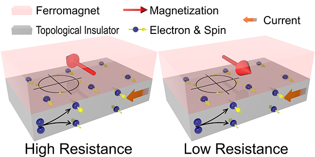
A new discovery, led by researchers at the University of Minnesota, demonstrates the existence of a new kind of magnetoresistance involving topological insulators that could result in improvements in future computing and computer storage. The details of their research are published in the most recent issue of the scientific journal Nature Communications (“Unidirectional spin-Hall and Rashba-Edelstein magnetoresistance in topological insulator-ferromagnet layer heterostructures”).

This image illustrates the work,

The schematic figure illustrates the concept and behavior of magnetoresistance. The spins are generated in topological insulators. Those at the interface between ferromagnet and topological insulators interact with the ferromagnet and result in either high or low resistance of the device, depending on the relative directions of magnetization and spins. Credit: University of Minnesota

A January 9, 2018 University of Minnesota College of Science and Engineering news release, which originated the news item, expands on the theme,

“Our discovery is one missing piece of the puzzle to improve the future of low-power computing and memory for the semiconductor industry, including brain-like computing and chips for robots and 3D magnetic memory,” said University of Minnesota Robert F. Hartmann Professor of Electrical and Computer Engineering Jian-Ping Wang, director of the Center for Spintronic Materials, Interfaces, and Novel Structures (C-SPIN) based at the University of Minnesota and co-author of the study.

Emerging technology using topological insulators

While magnetic recording still dominates data storage applications, the magnetoresistive random access memory is gradually finding its place in the field of computing memory. From the outside, they are unlike the hard disk drives which have mechanically spinning disks and swinging heads—they are more like any other type of memory. They are chips (solid state) which you’d find being soldered on circuit boards in a computer or mobile device.

Recently, a group of materials called topological insulators has been found to further improve the writing energy efficiency of magnetoresistive random access memory cells in electronics. However, the new device geometry demands a new magnetoresistance phenomenon to accomplish the read function of the memory cell in 3D system and network.

Following the recent discovery of the unidirectional spin Hall magnetoresistance in a conventional metal bilayer material systems, researchers at the University of Minnesota collaborated with colleagues at Pennsylvania State University and demonstrated for the first time the existence of such magnetoresistance in the topological insulator-ferromagnet bilayers.

The study confirms the existence of such unidirectional magnetoresistance and reveals that the adoption of topological insulators, compared to heavy metals, doubles the magnetoresistance performance at 150 Kelvin (-123.15 Celsius). From an application perspective, this work provides the missing piece of the puzzle to create a proposed 3D and cross-bar type computing and memory device involving topological insulators by adding the previously missing or very inconvenient read functionality.

In addition to Wang, researchers involved in this study include Yang Lv, Delin Zhang and Mahdi Jamali from the University of Minnesota Department of Electrical and Computer Engineering and James Kally, Joon Sue Lee and Nitin Samarth from Pennsylvania State University Department of Physics.

This research was funded by the Center for Spintronic Materials, Interfaces and Novel Architectures (C-SPIN) at the University of Minnesota, a Semiconductor Research Corporation program sponsored by the Microelectronics Advanced Research Corp. (MARCO) and the Defense Advanced Research Projects Agency (DARPA).

Here’s a link to and a citation for the paper,

Unidirectional spin-Hall and Rashba−Edelstein magnetoresistance in topological insulator-ferromagnet layer heterostructures by Yang Lv, James Kally, Delin Zhang, Joon Sue Lee, Mahdi Jamali, Nitin Samarth, & Jian-Ping Wang. Nature Communications 9, Article number: 111 (2018) doi:10.1038/s41467-017-02491-3 Published online: 09 January 2018

This is an open access paper.

Entanglement and biological systems

I think it was about five years ago thatI wrote a paper on something I called ‘cognitive entanglement’ (mentioned in my July 20,2012 posting) so the latest from Northwestern University (Chicago, Illinois, US) reignited my interest in entanglement. A December 5, 2017 news item on ScienceDaily describes the latest ‘entanglement’ research,

Nearly 75 years ago, Nobel Prize-winning physicist Erwin Schrödinger wondered if the mysterious world of quantum mechanics played a role in biology. A recent finding by Northwestern University’s Prem Kumar adds further evidence that the answer might be yes.

Kumar and his team have, for the first time, created quantum entanglement from a biological system. This finding could advance scientists’ fundamental understanding of biology and potentially open doors to exploit biological tools to enable new functions by harnessing quantum mechanics.

A December 5, 2017 Northwestern University news release (also on EurekAlert), which originated the news item, provides more detail,

“Can we apply quantum tools to learn about biology?” said Kumar, professor of electrical engineering and computer science in Northwestern’s McCormick School of Engineering and of physics and astronomy in the Weinberg College of Arts and Sciences. “People have asked this question for many, many years — dating back to the dawn of quantum mechanics. The reason we are interested in these new quantum states is because they allow applications that are otherwise impossible.”

Partially supported by the [US] Defense Advanced Research Projects Agency [DARPA], the research was published Dec. 5 [2017] in Nature Communications.

Quantum entanglement is one of quantum mechanics’ most mystifying phenomena. When two particles — such as atoms, photons, or electrons — are entangled, they experience an inexplicable link that is maintained even if the particles are on opposite sides of the universe. While entangled, the particles’ behavior is tied one another. If one particle is found spinning in one direction, for example, then the other particle instantaneously changes its spin in a corresponding manner dictated by the entanglement. Researchers, including Kumar, have been interested in harnessing quantum entanglement for several applications, including quantum communications. Because the particles can communicate without wires or cables, they could be used to send secure messages or help build an extremely fast “quantum Internet.”

“Researchers have been trying to entangle a larger and larger set of atoms or photons to develop substrates on which to design and build a quantum machine,” Kumar said. “My laboratory is asking if we can build these machines on a biological substrate.”

In the study, Kumar’s team used green fluorescent proteins, which are responsible for bioluminescence and commonly used in biomedical research. The team attempted to entangle the photons generated from the fluorescing molecules within the algae’s barrel-shaped protein structure by exposing them to spontaneous four-wave mixing, a process in which multiple wavelengths interact with one another to produce new wavelengths.

Through a series of these experiments, Kumar and his team successfully demonstrated a type of entanglement, called polarization entanglement, between photon pairs. The same feature used to make glasses for viewing 3D movies, polarization is the orientation of oscillations in light waves. A wave can oscillate vertically, horizontally, or at different angles. In Kumar’s entangled pairs, the photons’ polarizations are entangled, meaning that the oscillation directions of light waves are linked. Kumar also noticed that the barrel-shaped structure surrounding the fluorescing molecules protected the entanglement from being disrupted.

“When I measured the vertical polarization of one particle, we knew it would be the same in the other,” he said. “If we measured the horizontal polarization of one particle, we could predict the horizontal polarization in the other particle. We created an entangled state that correlated in all possibilities simultaneously.”

Now that they have demonstrated that it’s possible to create quantum entanglement from biological particles, next Kumar and his team plan to make a biological substrate of entangled particles, which could be used to build a quantum machine. Then, they will seek to understand if a biological substrate works more efficiently than a synthetic one.

Here’s an image accompanying the news release,

Featured in the cuvette on the left, green fluorescent proteins responsible for bioluninescence in jellyfish. Courtesy: Northwestern University

Here’s a link to and a citation for the paper,

Generation of photonic entanglement in green fluorescent proteins by Siyuan Shi, Prem Kumar & Kim Fook Lee. Nature Communications 8, Article number: 1934 (2017) doi:10.1038/s41467-017-02027-9 Published online: 05 December 2017

This paper is open access.

Leftover 2017 memristor news bits

i have two bits of news, one from this October 2017 about using light to control a memristor’s learning properties and one from December 2017 about memristors and neural networks.

Shining a light on the memristor

Michael Berger wrote an October 30, 2017 Nanowerk Sportlight article about some of the latest work concerning memristors and light,

Memristors – or resistive memory – are nanoelectronic devices that are very promising components for next generation memory and computing devices. They are two-terminal electric elements similar to a conventional resistor – however, the electric resistance in a memristor is dependent on the charge passing through it; which means that its conductance can be precisely modulated by charge or flux through it. Its special property is that its resistance can be programmed (resistor function) and subsequently remains stored (memory function).

In this sense, a memristor is similar to a synapse in the human brain because it exhibits the same switching characteristics, i.e. it is able, with a high level of plasticity, to modify the efficiency of signal transfer between neurons under the influence of the transfer itself. That’s why researchers are hopeful to use memristors for the fabrication of electronic synapses for neuromorphic (i.e. brain-like) computing that mimics some of the aspects of learning and computation in human brains.

Human brains may be slow at pure number crunching but they are excellent at handling fast dynamic sensory information such as image and voice recognition. Walking is something that we take for granted but this is quite challenging for robots, especially over uneven terrain.

“Memristors present an opportunity to make new types of computers that are different from existing von Neumann architectures, which traditional computers are based upon,” Dr Neil T. Kemp, a Lecturer in Physics at the University of Hull [UK], tells Nanowerk. “Our team at the University of Hull is focussed on making memristor devices dynamically reconfigurable and adaptive – we believe this is the route to making a new generation of artificial intelligence systems that are smarter and can exhibit complex behavior. Such systems would also have the advantage of memristors, high density integration and lower power usage, so these systems would be more lightweight, portable and not need re-charging so often – which is something really needed for robots etc.”

In their new paper in Nanoscale (“Reversible Optical Switching Memristors with Tunable STDP Synaptic Plasticity: A Route to Hierarchical Control in Artificial Intelligent Systems”), Kemp and his team demonstrate the ability to reversibly control the learning properties of memristors via optical means.

The reversibility is achieved by changing the polarization of light. The researchers have used this effect to demonstrate tuneable learning in a memristor. One way this is achieved is through something called Spike Timing Dependent Plasticity (STDP), which is an effect known to occur in human brains and is linked with sensory perception, spatial reasoning, language and conscious thought in the neocortex.

STDP learning is based upon differences in the arrival time of signals from two adjacent neurons. The University of Hull team has shown that they can modulate the synaptic plasticity via optical means which enables the devices to have tuneable learning.

“Our research findings are important because it demonstrates that light can be used to control the learning properties of a memristor,” Kemp points out. “We have shown that light can be used in a reversible manner to change the connection strength (or conductivity) of artificial memristor synapses and as well control their ability to forget i.e. we can dynamically change device to have short-term or long-term memory.”

According to the team, there are many potential applications, such as adaptive electronic circuits controllable via light, or in more complex systems, such as neuromorphic computing, the development of optically reconfigurable neural networks.

Having optically controllable memristors can also facilitate the implementation of hierarchical control in larger artificial-brain like systems, whereby some of the key processes that are carried out by biological molecules in human brains can be emulated in solid-state devices through patterning with light.

Some of these processes include synaptic pruning, conversion of short term memory to long term memory, erasing of certain memories that are no longer needed or changing the sensitivity of synapses to be more adept at learning new information.

“The ability to control this dynamically, both spatially and temporally, is particularly interesting since it would allow neural networks to be reconfigurable on the fly through either spatial patterning or by adjusting the intensity of the light source,” notes Kemp.

In their new paper in Nanoscale Currently, the devices are more suited to neuromorphic computing applications, which do not need to be as fast. Optical control of memristors opens the route to dynamically tuneable and reprogrammable synaptic circuits as well the ability (via optical patterning) to have hierarchical control in larger and more complex artificial intelligent systems.

“Artificial Intelligence is really starting to come on strong in many areas, especially in the areas of voice/image recognition and autonomous systems – we could even say that this is the next revolution, similarly to what the industrial revolution was to farming and production processes,” concludes Kemp. “There are many challenges to overcome though. …

That excerpt should give you the gist of Berger’s article and, for those who need more information, there’s Berger’s article and, also, a link to and a citation for the paper,

Reversible optical switching memristors with tunable STDP synaptic plasticity: a route to hierarchical control in artificial intelligent systems by Ayoub H. Jaafar, Robert J. Gray, Emanuele Verrelli, Mary O’Neill, Stephen. M. Kelly, and Neil T. Kemp. Nanoscale, 2017,9, 17091-17098 DOI: 10.1039/C7NR06138B First published on 24 Oct 2017

This paper is behind a paywall.

The memristor and the neural network

It would seem machine learning could experience a significant upgrade if the work in Wei Lu’s University of Michigan laboratory can be scaled for general use. From a December 22, 2017 news item on ScienceDaily,

A new type of neural network made with memristors can dramatically improve the efficiency of teaching machines to think like humans.

The network, called a reservoir computing system, could predict words before they are said during conversation, and help predict future outcomes based on the present.

The research team that created the reservoir computing system, led by Wei Lu, professor of electrical engineering and computer science at the University of Michigan, recently published their work in Nature Communications.

A December 19, 2017 University of Michigan news release (also on EurekAlert) by Dan Newman, which originated the news item, expands on the theme,

Reservoir computing systems, which improve on a typical neural network’s capacity and reduce the required training time, have been created in the past with larger optical components. However, the U-M group created their system using memristors, which require less space and can be integrated more easily into existing silicon-based electronics.

Memristors are a special type of resistive device that can both perform logic and store data. This contrasts with typical computer systems, where processors perform logic separate from memory modules. In this study, Lu’s team used a special memristor that memorizes events only in the near history.

Inspired by brains, neural networks are composed of neurons, or nodes, and synapses, the connections between nodes.

To train a neural network for a task, a neural network takes in a large set of questions and the answers to those questions. In this process of what’s called supervised learning, the connections between nodes are weighted more heavily or lightly to minimize the amount of error in achieving the correct answer.

Once trained, a neural network can then be tested without knowing the answer. For example, a system can process a new photo and correctly identify a human face, because it has learned the features of human faces from other photos in its training set.

“A lot of times, it takes days or months to train a network,” says Lu. “It is very expensive.”

Image recognition is also a relatively simple problem, as it doesn’t require any information apart from a static image. More complex tasks, such as speech recognition, can depend highly on context and require neural networks to have knowledge of what has just occurred, or what has just been said.

“When transcribing speech to text or translating languages, a word’s meaning and even pronunciation will differ depending on the previous syllables,” says Lu.

This requires a recurrent neural network, which incorporates loops within the network that give the network a memory effect. However, training these recurrent neural networks is especially expensive, Lu says.

Reservoir computing systems built with memristors, however, can skip most of the expensive training process and still provide the network the capability to remember. This is because the most critical component of the system – the reservoir – does not require training.

When a set of data is inputted into the reservoir, the reservoir identifies important time-related features of the data, and hands it off in a simpler format to a second network. This second network then only needs training like simpler neural networks, changing weights of the features and outputs that the first network passed on until it achieves an acceptable level of error.

Enlargereservoir computing system

IMAGE:  Schematic of a reservoir computing system, showing the reservoir with internal dynamics and the simpler output. Only the simpler output needs to be trained, allowing for quicker and lower-cost training. Courtesy Wei Lu.


“The beauty of reservoir computing is that while we design it, we don’t have to train it,” says Lu.

The team proved the reservoir computing concept using a test of handwriting recognition, a common benchmark among neural networks. Numerals were broken up into rows of pixels, and fed into the computer with voltages like Morse code, with zero volts for a dark pixel and a little over one volt for a white pixel.

Using only 88 memristors as nodes to identify handwritten versions of numerals, compared to a conventional network that would require thousands of nodes for the task, the reservoir achieved 91% accuracy.

Reservoir computing systems are especially adept at handling data that varies with time, like a stream of data or words, or a function depending on past results.

To demonstrate this, the team tested a complex function that depended on multiple past results, which is common in engineering fields. The reservoir computing system was able to model the complex function with minimal error.

Lu plans on exploring two future paths with this research: speech recognition and predictive analysis.

“We can make predictions on natural spoken language, so you don’t even have to say the full word,” explains Lu.

“We could actually predict what you plan to say next.”

In predictive analysis, Lu hopes to use the system to take in signals with noise, like static from far-off radio stations, and produce a cleaner stream of data. “It could also predict and generate an output signal even if the input stopped,” he says.

EnlargeWei Lu

IMAGE:  Wei Lu, Professor of Electrical Engineering & Computer Science at the University of Michigan holds a memristor he created. Photo: Marcin Szczepanski.


The work was published in Nature Communications in the article, “Reservoir computing using dynamic memristors for temporal information processing”, with authors Chao Du, Fuxi Cai, Mohammed Zidan, Wen Ma, Seung Hwan Lee, and Prof. Wei Lu.

The research is part of a $6.9 million DARPA [US Defense Advanced Research Projects Agency] project, called “Sparse Adaptive Local Learning for Sensing and Analytics [also known as SALLSA],” that aims to build a computer chip based on self-organizing, adaptive neural networks. The memristor networks are fabricated at Michigan’s Lurie Nanofabrication Facility.

Lu and his team previously used memristors in implementing “sparse coding,” which used a 32-by-32 array of memristors to efficiently analyze and recreate images.

Here’s a link to and a citation for the paper,

Reservoir computing using dynamic memristors for temporal information processing by Chao Du, Fuxi Cai, Mohammed A. Zidan, Wen Ma, Seung Hwan Lee & Wei D. Lu. Nature Communications 8, Article number: 2204 (2017) doi:10.1038/s41467-017-02337-y Published online: 19 December 2017

This is an open access paper.

Congratulate China on the world’s first quantum communication network

China has some exciting news about the world’s first quantum network; it’s due to open in late August 2017 so you may want to have your congratulations in order for later this month.

An Aug. 4, 2017 news item on phys.org makes the announcement,

As malicious hackers find ever more sophisticated ways to launch attacks, China is about to launch the Jinan Project, the world’s first unhackable computer network, and a major milestone in the development of quantum technology.

Named after the eastern Chinese city where the technology was developed, the network is planned to be fully operational by the end of August 2017. Jinan is the hub of the Beijing-Shanghai quantum network due to its strategic location between the two principal Chinese metropolises.

“We plan to use the network for national defence, finance and other fields, and hope to spread it out as a pilot that if successful can be used across China and the whole world,” commented Zhou Fei, assistant director of the Jinan Institute of Quantum Technology, who was speaking to Britain’s Financial Times.

An Aug. 3, 2017 CORDIS (Community Research and Development Research Information Service [for the European Commission]) press release, which originated the news item, provides more detail about the technology,

By launching the network, China will become the first country worldwide to implement quantum technology for a real life, commercial end. It also highlights that China is a key global player in the rush to develop technologies based on quantum principles, with the EU and the United States also vying for world leadership in the field.

The network, known as a Quantum Key Distribution (QKD) network, is more secure than widely used electronic communication equivalents. Unlike a conventional telephone or internet cable, which can be tapped without the sender or recipient being aware, a QKD network alerts both users to any tampering with the system as soon as it occurs. This is because tampering immediately alters the information being relayed, with the disturbance being instantly recognisable. Once fully implemented, it will make it almost impossible for other governments to listen in on Chinese communications.

In the Jinan network, some 200 users from China’s military, government, finance and electricity sectors will be able to send messages safe in the knowledge that only they are reading them. It will be the world’s longest land-based quantum communications network, stretching over 2 000 km.

Also speaking to the ‘Financial Times’, quantum physicist Tim Byrnes, based at New York University’s (NYU) Shanghai campus commented: ‘China has achieved staggering things with quantum research… It’s amazing how quickly China has gotten on with quantum research projects that would be too expensive to do elsewhere… quantum communication has been taken up by the commercial sector much more in China compared to other countries, which means it is likely to pull ahead of Europe and US in the field of quantum communication.’

However, Europe is also determined to also be at the forefront of the ‘quantum revolution’ which promises to be one of the major defining technological phenomena of the twenty-first century. The EU has invested EUR 550 million into quantum technologies and has provided policy support to researchers through the 2016 Quantum Manifesto.

Moreover, with China’s latest achievement (and a previous one already notched up from July 2017 when its quantum satellite – the world’s first – sent a message to Earth on a quantum communication channel), it looks like the race to be crowned the world’s foremost quantum power is well and truly underway…

Prior to this latest announcement, Chinese scientists had published work about quantum satellite communications, a development that makes their imminent terrestrial quantum network possible. Gabriel Popkin wrote about the quantum satellite in a June 15, 2017 article Science magazine,

Quantum entanglement—physics at its strangest—has moved out of this world and into space. In a study that shows China’s growing mastery of both the quantum world and space science, a team of physicists reports that it sent eerily intertwined quantum particles from a satellite to ground stations separated by 1200 kilometers, smashing the previous world record. The result is a stepping stone to ultrasecure communication networks and, eventually, a space-based quantum internet.

“It’s a huge, major achievement,” says Thomas Jennewein, a physicist at the University of Waterloo in Canada. “They started with this bold idea and managed to do it.”

Entanglement involves putting objects in the peculiar limbo of quantum superposition, in which an object’s quantum properties occupy multiple states at once: like Schrödinger’s cat, dead and alive at the same time. Then those quantum states are shared among multiple objects. Physicists have entangled particles such as electrons and photons, as well as larger objects such as superconducting electric circuits.

Theoretically, even if entangled objects are separated, their precarious quantum states should remain linked until one of them is measured or disturbed. That measurement instantly determines the state of the other object, no matter how far away. The idea is so counterintuitive that Albert Einstein mocked it as “spooky action at a distance.”

Starting in the 1970s, however, physicists began testing the effect over increasing distances. In 2015, the most sophisticated of these tests, which involved measuring entangled electrons 1.3 kilometers apart, showed once again that spooky action is real.

Beyond the fundamental result, such experiments also point to the possibility of hack-proof communications. Long strings of entangled photons, shared between distant locations, can be “quantum keys” that secure communications. Anyone trying to eavesdrop on a quantum-encrypted message would disrupt the shared key, alerting everyone to a compromised channel.

But entangled photons degrade rapidly as they pass through the air or optical fibers. So far, the farthest anyone has sent a quantum key is a few hundred kilometers. “Quantum repeaters” that rebroadcast quantum information could extend a network’s reach, but they aren’t yet mature. Many physicists have dreamed instead of using satellites to send quantum information through the near-vacuum of space. “Once you have satellites distributing your quantum signals throughout the globe, you’ve done it,” says Verónica Fernández Mármol, a physicist at the Spanish National Research Council in Madrid. …

Popkin goes on to detail the process for making the discovery in easily accessible (for the most part) writing and in a video and a graphic.

Russell Brandom writing for The Verge in a June 15, 2017 article about the Chinese quantum satellite adds detail about previous work and teams in other countries also working on the challenge (Note: Links have been removed),

Quantum networking has already shown promise in terrestrial fiber networks, where specialized routing equipment can perform the same trick over conventional fiber-optic cable. The first such network was a DARPA-funded connection established in 2003 between Harvard, Boston University, and a private lab. In the years since, a number of companies have tried to build more ambitious connections. The Swiss company ID Quantique has mapped out a quantum network that would connect many of North America’s largest data centers; in China, a separate team is working on a 2,000-kilometer quantum link between Beijing and Shanghai, which would rely on fiber to span an even greater distance than the satellite link. Still, the nature of fiber places strict limits on how far a single photon can travel.

According to ID Quantique, a reliable satellite link could connect the existing fiber networks into a single globe-spanning quantum network. “This proves the feasibility of quantum communications from space,” ID Quantique CEO Gregoire Ribordy tells The Verge. “The vision is that you have regional quantum key distribution networks over fiber, which can connect to each other through the satellite link.”

China isn’t the only country working on bringing quantum networks to space. A collaboration between the UK’s University of Strathclyde and the National University of Singapore is hoping to produce the same entanglement in cheap, readymade satellites called Cubesats. A Canadian team is also developing a method of producing entangled photons on the ground before sending them into space.

I wonder if there’s going to be an invitational event for scientists around the world to celebrate the launch.

3-D integration of nanotechnologies on a single computer chip

By integrating nanomaterials , a new technique for a 3D computer chip capable of handling today’s huge amount of data has been developed. Weirdly, the first two paragraphs of a July 5, 2017 news item on Nanowerk do not convey the main point (Note: A link has been removed),

As embedded intelligence is finding its way into ever more areas of our lives, fields ranging from autonomous driving to personalized medicine are generating huge amounts of data. But just as the flood of data is reaching massive proportions, the ability of computer chips to process it into useful information is stalling.

Now, researchers at Stanford University and MIT have built a new chip to overcome this hurdle. The results are published today in the journal Nature (“Three-dimensional integration of nanotechnologies for computing and data storage on a single chip”), by lead author Max Shulaker, an assistant professor of electrical engineering and computer science at MIT. Shulaker began the work as a PhD student alongside H.-S. Philip Wong and his advisor Subhasish Mitra, professors of electrical engineering and computer science at Stanford. The team also included professors Roger Howe and Krishna Saraswat, also from Stanford.

This image helps to convey the main points,

Instead of relying on silicon-based devices, a new chip uses carbon nanotubes and resistive random-access memory (RRAM) cells. The two are built vertically over one another, making a new, dense 3-D computer architecture with interleaving layers of logic and memory. Courtesy MIT

As I hove been quite impressed with their science writing, it was a bit surprising to find that the Massachusetts Institute of Technology (MIT) had issued this news release (news item) as it didn’t follow the ‘rules’, i.e., cover as many of the journalistic questions (Who, What, Where, When, Why, and, sometimes, How) as possible in the first sentence/paragraph. This is written more in the style of a magazine article and so the details take a while to emerge, from a July 5, 2017 MIT news release, which originated the news item,

Computers today comprise different chips cobbled together. There is a chip for computing and a separate chip for data storage, and the connections between the two are limited. As applications analyze increasingly massive volumes of data, the limited rate at which data can be moved between different chips is creating a critical communication “bottleneck.” And with limited real estate on the chip, there is not enough room to place them side-by-side, even as they have been miniaturized (a phenomenon known as Moore’s Law).

To make matters worse, the underlying devices, transistors made from silicon, are no longer improving at the historic rate that they have for decades.

The new prototype chip is a radical change from today’s chips. It uses multiple nanotechnologies, together with a new computer architecture, to reverse both of these trends.

Instead of relying on silicon-based devices, the chip uses carbon nanotubes, which are sheets of 2-D graphene formed into nanocylinders, and resistive random-access memory (RRAM) cells, a type of nonvolatile memory that operates by changing the resistance of a solid dielectric material. The researchers integrated over 1 million RRAM cells and 2 million carbon nanotube field-effect transistors, making the most complex nanoelectronic system ever made with emerging nanotechnologies.

The RRAM and carbon nanotubes are built vertically over one another, making a new, dense 3-D computer architecture with interleaving layers of logic and memory. By inserting ultradense wires between these layers, this 3-D architecture promises to address the communication bottleneck.

However, such an architecture is not possible with existing silicon-based technology, according to the paper’s lead author, Max Shulaker, who is a core member of MIT’s Microsystems Technology Laboratories. “Circuits today are 2-D, since building conventional silicon transistors involves extremely high temperatures of over 1,000 degrees Celsius,” says Shulaker. “If you then build a second layer of silicon circuits on top, that high temperature will damage the bottom layer of circuits.”

The key in this work is that carbon nanotube circuits and RRAM memory can be fabricated at much lower temperatures, below 200 C. “This means they can be built up in layers without harming the circuits beneath,” Shulaker says.

This provides several simultaneous benefits for future computing systems. “The devices are better: Logic made from carbon nanotubes can be an order of magnitude more energy-efficient compared to today’s logic made from silicon, and similarly, RRAM can be denser, faster, and more energy-efficient compared to DRAM,” Wong says, referring to a conventional memory known as dynamic random-access memory.

“In addition to improved devices, 3-D integration can address another key consideration in systems: the interconnects within and between chips,” Saraswat adds.

“The new 3-D computer architecture provides dense and fine-grained integration of computating and data storage, drastically overcoming the bottleneck from moving data between chips,” Mitra says. “As a result, the chip is able to store massive amounts of data and perform on-chip processing to transform a data deluge into useful information.”

To demonstrate the potential of the technology, the researchers took advantage of the ability of carbon nanotubes to also act as sensors. On the top layer of the chip they placed over 1 million carbon nanotube-based sensors, which they used to detect and classify ambient gases.

Due to the layering of sensing, data storage, and computing, the chip was able to measure each of the sensors in parallel, and then write directly into its memory, generating huge bandwidth, Shulaker says.

Three-dimensional integration is the most promising approach to continue the technology scaling path set forth by Moore’s laws, allowing an increasing number of devices to be integrated per unit volume, according to Jan Rabaey, a professor of electrical engineering and computer science at the University of California at Berkeley, who was not involved in the research.

“It leads to a fundamentally different perspective on computing architectures, enabling an intimate interweaving of memory and logic,” Rabaey says. “These structures may be particularly suited for alternative learning-based computational paradigms such as brain-inspired systems and deep neural nets, and the approach presented by the authors is definitely a great first step in that direction.”

“One big advantage of our demonstration is that it is compatible with today’s silicon infrastructure, both in terms of fabrication and design,” says Howe.

“The fact that this strategy is both CMOS [complementary metal-oxide-semiconductor] compatible and viable for a variety of applications suggests that it is a significant step in the continued advancement of Moore’s Law,” says Ken Hansen, president and CEO of the Semiconductor Research Corporation, which supported the research. “To sustain the promise of Moore’s Law economics, innovative heterogeneous approaches are required as dimensional scaling is no longer sufficient. This pioneering work embodies that philosophy.”

The team is working to improve the underlying nanotechnologies, while exploring the new 3-D computer architecture. For Shulaker, the next step is working with Massachusetts-based semiconductor company Analog Devices to develop new versions of the system that take advantage of its ability to carry out sensing and data processing on the same chip.

So, for example, the devices could be used to detect signs of disease by sensing particular compounds in a patient’s breath, says Shulaker.

“The technology could not only improve traditional computing, but it also opens up a whole new range of applications that we can target,” he says. “My students are now investigating how we can produce chips that do more than just computing.”

“This demonstration of the 3-D integration of sensors, memory, and logic is an exceptionally innovative development that leverages current CMOS technology with the new capabilities of carbon nanotube field–effect transistors,” says Sam Fuller, CTO emeritus of Analog Devices, who was not involved in the research. “This has the potential to be the platform for many revolutionary applications in the future.”

This work was funded by the Defense Advanced Research Projects Agency [DARPA], the National Science Foundation, Semiconductor Research Corporation, STARnet SONIC, and member companies of the Stanford SystemX Alliance.

Here’s a link to and a citation for the paper,

Three-dimensional integration of nanotechnologies for computing and data storage on a single chip by Max M. Shulaker, Gage Hills, Rebecca S. Park, Roger T. Howe, Krishna Saraswat, H.-S. Philip Wong, & Subhasish Mitra. Nature 547, 74–78 (06 July 2017) doi:10.1038/nature22994 Published online 05 July 2017

This paper is behind a paywall.

IBM to build brain-inspired AI supercomputing system equal to 64 million neurons for US Air Force

This is the second IBM computer announcement I’ve stumbled onto within the last 4 weeks or so,  which seems like a veritable deluge given the last time I wrote about IBM’s computing efforts was in an Oct. 8, 2015 posting about carbon nanotubes,. I believe that up until now that was my  most recent posting about IBM and computers.

Moving onto the news, here’s more from a June 23, 3017 news item on Nanotechnology Now,

IBM (NYSE: IBM) and the U.S. Air Force Research Laboratory (AFRL) today [June 23, 2017] announced they are collaborating on a first-of-a-kind brain-inspired supercomputing system powered by a 64-chip array of the IBM TrueNorth Neurosynaptic System. The scalable platform IBM is building for AFRL will feature an end-to-end software ecosystem designed to enable deep neural-network learning and information discovery. The system’s advanced pattern recognition and sensory processing power will be the equivalent of 64 million neurons and 16 billion synapses, while the processor component will consume the energy equivalent of a dim light bulb – a mere 10 watts to power.

A June 23, 2017 IBM news release, which originated the news item, describes the proposed collaboration, which is based on IBM’s TrueNorth brain-inspired chip architecture (see my Aug. 8, 2014 posting for more about TrueNorth),

IBM researchers believe the brain-inspired, neural network design of TrueNorth will be far more efficient for pattern recognition and integrated sensory processing than systems powered by conventional chips. AFRL is investigating applications of the system in embedded, mobile, autonomous settings where, today, size, weight and power (SWaP) are key limiting factors.

The IBM TrueNorth Neurosynaptic System can efficiently convert data (such as images, video, audio and text) from multiple, distributed sensors into symbols in real time. AFRL will combine this “right-brain” perception capability of the system with the “left-brain” symbol processing capabilities of conventional computer systems. The large scale of the system will enable both “data parallelism” where multiple data sources can be run in parallel against the same neural network and “model parallelism” where independent neural networks form an ensemble that can be run in parallel on the same data.

“AFRL was the earliest adopter of TrueNorth for converting data into decisions,” said Daniel S. Goddard, director, information directorate, U.S. Air Force Research Lab. “The new neurosynaptic system will be used to enable new computing capabilities important to AFRL’s mission to explore, prototype and demonstrate high-impact, game-changing technologies that enable the Air Force and the nation to maintain its superior technical advantage.”

“The evolution of the IBM TrueNorth Neurosynaptic System is a solid proof point in our quest to lead the industry in AI hardware innovation,” said Dharmendra S. Modha, IBM Fellow, chief scientist, brain-inspired computing, IBM Research – Almaden. “Over the last six years, IBM has expanded the number of neurons per system from 256 to more than 64 million – an 800 percent annual increase over six years.’’

The system fits in a 4U-high (7”) space in a standard server rack and eight such systems will enable the unprecedented scale of 512 million neurons per rack. A single processor in the system consists of 5.4 billion transistors organized into 4,096 neural cores creating an array of 1 million digital neurons that communicate with one another via 256 million electrical synapses.    For CIFAR-100 dataset, TrueNorth achieves near state-of-the-art accuracy, while running at >1,500 frames/s and using 200 mW (effectively >7,000 frames/s per Watt) – orders of magnitude lower speed and energy than a conventional computer running inference on the same neural network.

The IBM TrueNorth Neurosynaptic System was originally developed under the auspices of Defense Advanced Research Projects Agency’s (DARPA) Systems of Neuromorphic Adaptive Plastic Scalable Electronics (SyNAPSE) program in collaboration with Cornell University. In 2016, the TrueNorth Team received the inaugural Misha Mahowald Prize for Neuromorphic Engineering and TrueNorth was accepted into the Computer History Museum.  Research with TrueNorth is currently being performed by more than 40 universities, government labs, and industrial partners on five continents.

There is an IBM video accompanying this news release, which seems more promotional than informational,

The IBM scientist featured in the video has a Dec. 19, 2016 posting on an IBM research blog which provides context for this collaboration with AFRL,

2016 was a big year for brain-inspired computing. My team and I proved in our paper “Convolutional networks for fast, energy-efficient neuromorphic computing” that the value of this breakthrough is that it can perform neural network inference at unprecedented ultra-low energy consumption. Simply stated, our TrueNorth chip’s non-von Neumann architecture mimics the brain’s neural architecture — giving it unprecedented efficiency and scalability over today’s computers.

The brain-inspired TrueNorth processor [is] a 70mW reconfigurable silicon chip with 1 million neurons, 256 million synapses, and 4096 parallel and distributed neural cores. For systems, we present a scale-out system loosely coupling 16 single-chip boards and a scale-up system tightly integrating 16 chips in a 4´4 configuration by exploiting TrueNorth’s native tiling.

For the scale-up systems we summarize our approach to physical placement of neural network, to reduce intra- and inter-chip network traffic. The ecosystem is in use at over 30 universities and government / corporate labs. Our platform is a substrate for a spectrum of applications from mobile and embedded computing to cloud and supercomputers.
TrueNorth Ecosystem for Brain-Inspired Computing: Scalable Systems, Software, and Applications

TrueNorth, once loaded with a neural network model, can be used in real-time as a sensory streaming inference engine, performing rapid and accurate classifications while using minimal energy. TrueNorth’s 1 million neurons consume only 70 mW, which is like having a neurosynaptic supercomputer the size of a postage stamp that can run on a smartphone battery for a week.

Recently, in collaboration with Lawrence Livermore National Laboratory, U.S. Air Force Research Laboratory, and U.S. Army Research Laboratory, we published our fifth paper at IEEE’s prestigious Supercomputing 2016 conference that summarizes the results of the team’s 12.5-year journey (see the associated graphic) to unlock this value proposition. [keep scrolling for the graphic]

Applying the mind of a chip

Three of our partners, U.S. Army Research Lab, U.S. Air Force Research Lab and Lawrence Livermore National Lab, contributed sections to the Supercomputing paper each showcasing a different TrueNorth system, as summarized by my colleagues Jun Sawada, Brian Taba, Pallab Datta, and Ben Shaw:

U.S. Army Research Lab (ARL) prototyped a computational offloading scheme to illustrate how TrueNorth’s low power profile enables computation at the point of data collection. Using the single-chip NS1e board and an Android tablet, ARL researchers created a demonstration system that allows visitors to their lab to hand write arithmetic expressions on the tablet, with handwriting streamed to the NS1e for character recognition, and recognized characters sent back to the tablet for arithmetic calculation.

Of course, the point here is not to make a handwriting calculator, it is to show how TrueNorth’s low power and real time pattern recognition might be deployed at the point of data collection to reduce latency, complexity and transmission bandwidth, as well as back-end data storage requirements in distributed systems.

U.S. Air Force Research Lab (AFRL) contributed another prototype application utilizing a TrueNorth scale-out system to perform a data-parallel text extraction and recognition task. In this application, an image of a document is segmented into individual characters that are streamed to AFRL’s NS1e16 TrueNorth system for parallel character recognition. Classification results are then sent to an inference-based natural language model to reconstruct words and sentences. This system can process 16,000 characters per second! AFRL plans to implement the word and sentence inference algorithms on TrueNorth, as well.

Lawrence Livermore National Lab (LLNL) has a 16-chip NS16e scale-up system to explore the potential of post-von Neumann computation through larger neural models and more complex algorithms, enabled by the native tiling characteristics of the TrueNorth chip. For the Supercomputing paper, they contributed a single-chip application performing in-situ process monitoring in an additive manufacturing process. LLNL trained a TrueNorth network to recognize seven classes related to track weld quality in welds produced by a selective laser melting machine. Real-time weld quality determination allows for closed-loop process improvement and immediate rejection of defective parts. This is one of several applications LLNL is developing to showcase TrueNorth as a scalable platform for low-power, real-time inference.

[downloaded from https://www.ibm.com/blogs/research/2016/12/the-brains-architecture-efficiency-on-a-chip/] Courtesy: IBM

I gather this 2017 announcement is the latest milestone on the TrueNorth journey.