Tag Archives: Samsung

Synaptic transistors for brainlike computers based on (more environmentally friendly) graphene

An August 9, 2022 news item on ScienceDaily describes research investigating materials other than silicon for neuromorphic (brainlike) computing purposes,

Computers that think more like human brains are inching closer to mainstream adoption. But many unanswered questions remain. Among the most pressing, what types of materials can serve as the best building blocks to unlock the potential of this new style of computing.

For most traditional computing devices, silicon remains the gold standard. However, there is a movement to use more flexible, efficient and environmentally friendly materials for these brain-like devices.

In a new paper, researchers from The University of Texas at Austin developed synaptic transistors for brain-like computers using the thin, flexible material graphene. These transistors are similar to synapses in the brain, that connect neurons to each other.

An August 8, 2022 University of Texas at Austin news release (also on EurekAlert but published August 9, 2022), which originated the news item, provides more detail about the research,

“Computers that think like brains can do so much more than today’s devices,” said Jean Anne Incorvia, an assistant professor in the Cockrell School of Engineering’s Department of Electrical and Computer Engineer and the lead author on the paper published today in Nature Communications. “And by mimicking synapses, we can teach these devices to learn on the fly, without requiring huge training methods that take up so much power.”

The Research: A combination of graphene and nafion, a polymer membrane material, make up the backbone of the synaptic transistor. Together, these materials demonstrate key synaptic-like behaviors — most importantly, the ability for the pathways to strengthen over time as they are used more often, a type of neural muscle memory. In computing, this means that devices will be able to get better at tasks like recognizing and interpreting images over time and do it faster.

Another important finding is that these transistors are biocompatible, which means they can interact with living cells and tissue. That is key for potential applications in medical devices that come into contact with the human body. Most materials used for these early brain-like devices are toxic, so they would not be able to contact living cells in any way.

Why It Matters: With new high-tech concepts like self-driving cars, drones and robots, we are reaching the limits of what silicon chips can efficiently do in terms of data processing and storage. For these next-generation technologies, a new computing paradigm is needed. Neuromorphic devices mimic processing capabilities of the brain, a powerful computer for immersive tasks.

“Biocompatibility, flexibility, and softness of our artificial synapses is essential,” said Dmitry Kireev, a post-doctoral researcher who co-led the project. “In the future, we envision their direct integration with the human brain, paving the way for futuristic brain prosthesis.”

Will It Really Happen: Neuromorphic platforms are starting to become more common. Leading chipmakers such as Intel and Samsung have either produced neuromorphic chips already or are in the process of developing them. However, current chip materials place limitations on what neuromorphic devices can do, so academic researchers are working hard to find the perfect materials for soft brain-like computers.

“It’s still a big open space when it comes to materials; it hasn’t been narrowed down to the next big solution to try,” Incorvia said. “And it might not be narrowed down to just one solution, with different materials making more sense for different applications.”

The Team: The research was led by Incorvia and Deji Akinwande, professor in the Department of Electrical and Computer Engineering. The two have collaborated many times together in the past, and Akinwande is a leading expert in graphene, using it in multiple research breakthroughs, most recently as part of a wearable electronic tattoo for blood pressure monitoring.

The idea for the project was conceived by Samuel Liu, a Ph.D. student and first author on the paper, in a class taught by Akinwande. Kireev then suggested the specific project. Harrison Jin, an undergraduate electrical and computer engineering student, measured the devices and analyzed data.

The team collaborated with T. Patrick Xiao and Christopher Bennett of Sandia National Laboratories, who ran neural network simulations and analyzed the resulting data.

Here’s a link to and a citation for the ‘graphene transistor’ paper,

Metaplastic and energy-efficient biocompatible graphene artificial synaptic transistors for enhanced accuracy neuromorphic computing by Dmitry Kireev, Samuel Liu, Harrison Jin, T. Patrick Xiao, Christopher H. Bennett, Deji Akinwande & Jean Anne C. Incorvia. Nature Communications volume 13, Article number: 4386 (2022) DOI: https://doi.org/10.1038/s41467-022-32078-6 Published: 28 July 2022

This paper is open access.

Art and 5G at museums in Turin (Italy)

Caption: In the framework of EU-funded project 5GTours, R1 humanoid robot tested at GAM (Turin) its ability to navigate and interact with visitors at the 20th-century collections, accompanying them to explore a selection of the museum’s most representative works, such as Andy Warhol’s “Orange car crash”. The robot has been designed and developed by IIT, while the 5G connection was set up by TIM using Ericsson technology.. Credit: IIT-Istituto Italiano di Tecnologia/GAM

This May 27, 2022 Istituto Italiano di Tecnologia (IIT) press release on EurekAlert offers an intriguing view into the potential for robots in art galleries,

Robotics, 5G and art: during the month of May visitors to the Turin’s art museums, Turin Civic Gallery of Modern and Contemporary Art (GAM) and Turin City Museum of Ancient Art (Palazzo Madama), had the opportunity to be part of various experiments based on 5G-network technology. Interactive technologies and robots were the focus of an innovative enjoyment of the art collections, with a great appreciation from the public.

Visitors to the GAM and to Palazzo Madama were provided with a number of engaging interactive experiences made possible through a significant collaboration between public and private organisations, which have been working together for more than three years to experiment the potential of new 5G technology in the framework of the EU-funded project 5GTours (https://5gtours.eu/).

The demonstrations set up in Turin led to the creation of innovative applications in the tourism and culture sectors that can easily be replicated in any artistic or museum context.

In both venues, visitors had the opportunity to meet R1, the humanoid robot designed by the IIT-Istituto Italiano di Tecnologia (Italian Institute of Technology) in Genova and created to operate in domestic and professional environments, whose autonomous and remote navigation system is well integrated with the bandwidth and latency offered by a 5G connection. R1, the robot – 1 metre 25 cm in height, weighing 50 kg, made 50% from plastic and 50% from carbon fibre and metal – is able to describe the works and answer questions regarding the artist or the period in history to which the work belongs. 5G connectivity is required in order to transmit the considerable quantity of data generated by the robot’s sensors and the algorithms that handle environmental perception, autonomous navigation and dialogue to external processing systems with extremely rapid response times.

At Palazzo Madama R1 humanoid robot led a guided tour of the Ceramics Room, while at GAM it was available to visitors of the twentieth-century collections, accompanying them to explore a selection of the museum’s most representative works. R1 robot explained and responded to questions about six relevant paintings: Felice Casorati’s “Daphne a Pavarolo”, Osvaldo Lucini’s “Uccello 2”, Marc Chagall’s “Dans mon pays”, Alberto Burri’s “Sacco”, Andy Warhol’s “Orange car crash” and Mario Merz’s “Che Fare?”.

Moreover, visitors – with the use of Meta Quest visors also connected to the 5G network – were required to solve a puzzle, putting the paintings in the Guards’ Room back into their frames. With these devices, the works in the hall, which in reality cannot be touched, can be handled and moved virtually. Lastly, the visitors involved had the opportunity to visit the underground spaces of Palazzo Madama with the mini-robot Double 3, which uses the 5G network to move reactively and precisely within the narrow spaces.

At GAM a class of students from a local school were able to remotely connect and manoeuvre the mini-robot Double 3 located in the rooms of the twentieth-century collections at the GAM directly from their classroom. A treasure hunt held in the museum with the participants never leaving the school.

In the Educational Area, a group of youngsters had the opportunity of collaborating in the painting of a virtual work of art on a large technological wall, drawing inspiration from works by Nicola De Maria.

The 5G network solutions created at the GAM and at Palazzo Madama by TIM [Telecom Italia] with Ericsson technology in collaboration with the City of Turin and the Turin Museum Foundation, guarantee constant high-speed transmission and extremely low latency. These solutions, which comply with 3GPP standard, are extremely flexible in terms of setting up and use. In the case of Palazzo Madama, a UNESCO World Heritage Site, tailor-made installations were designed, using apparatus and solutions that perfectly integrate with the museum spaces, while at the same time guaranteeing extremely high performance. At the GAM, the Radio Dot System has been implemented, a new 5G solution from Ericsson that is small enough to be held in the palm of a hand, and that provides network coverage and performance required for busy indoor areas. Thanks to these activities, Turin is ever increasingly playing a role as an open-air laboratory for urban innovation; since 2021 it has been the location of the “House of Emerging Technology – CTE NEXT”, a veritable centre for technology transfer via 5G and for emerging technologies coordinated by the Municipality of Turin and financed by the Ministry for Economic Development.

Through these solutions, Palazzo Madama and the GAM are now unique examples of technology in Italy and a rare example on a European level of museum buildings with full 5G coverage.

The experience was the result of the project financed by the European Union, 5G-TOURS 5G smarT mObility, media and e-health for toURists and citizenS”, the city of Turin – Department and Directorate of Innovation, in collaboration with the Department of Culture – Ericsson, TIM [Telecom Italia], the Turin Museum Foundation and the IIT-Istituto Italiano di Tecnologia (Italian Institute of Technology) of Genova, with the contribution of the international partners Atos and Samsung. The 5G coverage within the two museums was set up by TIM using Ericsson technology, solutions that perfectly integrated with the areas within the two museums structures.

Just in case you missed the link in the press release, you can find more information about this European Union Horizon 2020-funded 5G project, here at 5G TOURS (SmarT mObility, media and e-health for toURists and citizenS). You can find out more about the grant, e.g., this project sunset in July 2022, here.

New design directions to increase variety, efficiency, selectivity and reliability for memristive devices

A May 11, 2020 news item on ScienceDaily provides a description of the current ‘memristor scene’ along with an announcement about a piece of recent research,

Scientists around the world are intensively working on memristive devices, which are capable in extremely low power operation and behave similarly to neurons in the brain. Researchers from the Jülich Aachen Research Alliance (JARA) and the German technology group Heraeus have now discovered how to systematically control the functional behaviour of these elements. The smallest differences in material composition are found crucial: differences so small that until now experts had failed to notice them. The researchers’ design directions could help to increase variety, efficiency, selectivity and reliability for memristive technology-based applications, for example for energy-efficient, non-volatile storage devices or neuro-inspired computers.

Memristors are considered a highly promising alternative to conventional nanoelectronic elements in computer Chips [sic]. Because of the advantageous functionalities, their development is being eagerly pursued by many companies and research institutions around the world. The Japanese corporation NEC installed already the first prototypes in space satellites back in 2017. Many other leading companies such as Hewlett Packard, Intel, IBM, and Samsung are working to bring innovative types of computer and storage devices based on memristive elements to market.

Fundamentally, memristors are simply “resistors with memory,” in which high resistance can be switched to low resistance and back again. This means in principle that the devices are adaptive, similar to a synapse in a biological nervous system. “Memristive elements are considered ideal candidates for neuro-inspired computers modelled on the brain, which are attracting a great deal of interest in connection with deep learning and artificial intelligence,” says Dr. Ilia Valov of the Peter Grünberg Institute (PGI-7) at Forschungszentrum Jülich.

In the latest issue of the open access journal Science Advances, he and his team describe how the switching and neuromorphic behaviour of memristive elements can be selectively controlled. According to their findings, the crucial factor is the purity of the switching oxide layer. “Depending on whether you use a material that is 99.999999 % pure, and whether you introduce one foreign atom into ten million atoms of pure material or into one hundred atoms, the properties of the memristive elements vary substantially” says Valov.

A May 11, 2020 Forschungszentrum Juelich press release (also on EurekAlert), which originated the news item, delves into the theme of increasing control over memristive systems,

This effect had so far been overlooked by experts. It can be used very specifically for designing memristive systems, in a similar way to doping semiconductors in information technology. “The introduction of foreign atoms allows us to control the solubility and transport properties of the thin oxide layers,” explains Dr. Christian Neumann of the technology group Heraeus. He has been contributing his materials expertise to the project ever since the initial idea was conceived in 2015.

“In recent years there has been remarkable progress in the development and use of memristive devices, however that progress has often been achieved on a purely empirical basis,” according to Valov. Using the insights that his team has gained, manufacturers could now methodically develop memristive elements selecting the functions they need. The higher the doping concentration, the slower the resistance of the elements changes as the number of incoming voltage pulses increases and decreases, and the more stable the resistance remains. “This means that we have found a way for designing types of artificial synapses with differing excitability,” explains Valov.

Design specification for artificial synapses

The brain’s ability to learn and retain information can largely be attributed to the fact that the connections between neurons are strengthened when they are frequently used. Memristive devices, of which there are different types such as electrochemical metallization cells (ECMs) or valence change memory cells (VCMs), behave similarly. When these components are used, the conductivity increases as the number of incoming voltage pulses increases. The changes can also be reversed by applying voltage pulses of the opposite polarity.

The JARA researchers conducted their systematic experiments on ECMs, which consist of a copper electrode, a platinum electrode, and a layer of silicon dioxide between them. Thanks to the cooperation with Heraeus researchers, the JARA scientists had access to different types of silicon dioxide: one with a purity of 99.999999 % – also called 8N silicon dioxide – and others containing 100 to 10,000 ppm (parts per million) of foreign atoms. The precisely doped glass used in their experiments was specially developed and manufactured by quartz glass specialist Heraeus Conamic, which also holds the patent for the procedure. Copper and protons acted as mobile doping agents, while aluminium and gallium were used as non-volatile doping.

Synapses, the connections between neurons, have the ability to transmit signals with varying degrees of strength when they are excited by a quick succession of electrical impulses. One effect of this repeated activity is to increase the concentration of calcium ions, with the result that more neurotransmitters are emitted. Depending on the activity, other effects cause long-term structural changes, which impact the strength of the transmission for several hours, or potentially even for the rest of the person’s life. Memristive elements allow the strength of the electrical transmission to be changed in a similar way to synaptic connections, by applying a voltage. In electrochemical metallization cells (ECMs), a metallic filament develops between the two metal electrodes, thus increasing conductivity. Applying voltage pulses with reversed polarity causes the filament to shrink again until the cell reaches its initial high resistance state. Copyright: Forschungszentrum Jülich / Tobias Schlößer

Record switching time confirms theory

Based on their series of experiments, the researchers were able to show that the ECMs’ switching times change as the amount of doping atoms changes. If the switching layer is made of 8N silicon dioxide, the memristive component switches in only 1.4 nanoseconds. To date, the fastest value ever measured for ECMs had been around 10 nanoseconds. By doping the oxide layer of the components with up to 10,000 ppm of foreign atoms, the switching time was prolonged into the range of milliseconds. “We can also theoretically explain our results. This is helping us to understand the physico-chemical processes on the nanoscale and apply this knowledge in the practice” says Valov. Based on generally applicable theoretical considerations, supported by experimental results, some also documented in the literature, he is convinced that the doping/impurity effect occurs and can be employed in all types memristive elements.

Top: In memristive elements (ECMs) with an undoped, high-purity switching layer of silicon oxide (SiO2), copper ions can move very fast. A filament of copper atoms forms correspondingly fast on the platinum electrode. This increases the total device conductivity respectively the capacity. Due to the high mobility of the ions, however, this filament is unstable at low forming voltages. Center: Gallium ions (Ga3+), which are introduced into the cell (non-volatile doping), bind copper ions (Cu2+) in the switching layer. The movement of the ions slows down, leading to lower switching times, but the filament, once formed remains longer stable. Bottom: Doping with aluminium ions (Al3+) slows down the process even more, since aluminium ions bind copper ions even stronger than gallium ions. Filament growth is even slower, while at the same time the stability of the filament is further increased. Depending on the chemical properties of the introduced doping elements, memristive cells – the artificial synapses – can be created with tailor-made switching and neuromorphic properties. Copyright: Forschungszentrum Jülich / Tobias Schloesser

Here’s a link to and a citation for the paper,

Design of defect-chemical properties and device performance in memristive systems by M. Lübben, F. Cüppers, J. Mohr, M. von Witzleben, U. Breuer, R. Waser, C. Neumann, and I. Valov. Science Advances 08 May 2020: Vol. 6, no. 19, eaaz9079 DOI: 10.1126/sciadv.aaz9079

This paper is open access.

For anyone curious about the German technology group, Heraeus, there’s a fascinating history in its Wikipedia entry. The technology company was formally founded in 1851 but it can be traced back to the 17th century and the founding family’s apothecary.

7nm (nanometre) chip shakeup

From time to time I check out the latest on attempts to shrink computer chips. In my July 11, 2014 posting I noted IBM’s announcement about developing a 7nm computer chip and later in my July 15, 2015 posting I noted IBM’s announcement of a working 7nm chip (from a July 9, 2015 IBM news release , “The breakthrough, accomplished in partnership with GLOBALFOUNDRIES and Samsung at SUNY Polytechnic Institute’s Colleges of Nanoscale Science and Engineering (SUNY Poly CNSE), could result in the ability to place more than 20 billion tiny switches — transistors — on the fingernail-sized chips that power everything from smartphones to spacecraft.”

I’m not sure what happened to the IBM/Global Foundries/Samsung partnership but Global Foundries recently announced that it will no longer be working on 7nm chips. From an August 27, 2018 Global Foundries news release,

GLOBALFOUNDRIES [GF] today announced an important step in its transformation, continuing the trajectory launched with the appointment of Tom Caulfield as CEO earlier this year. In line with the strategic direction Caulfield has articulated, GF is reshaping its technology portfolio to intensify its focus on delivering truly differentiated offerings for clients in high-growth markets.

GF is realigning its leading-edge FinFET roadmap to serve the next wave of clients that will adopt the technology in the coming years. The company will shift development resources to make its 14/12nm FinFET platform more relevant to these clients, delivering a range of innovative IP and features including RF, embedded memory, low power and more. To support this transition, GF is putting its 7nm FinFET program on hold indefinitely [emphasis mine] and restructuring its research and development teams to support its enhanced portfolio initiatives. This will require a workforce reduction, however a significant number of top technologists will be redeployed on 14/12nm FinFET derivatives and other differentiated offerings.

I tried to find a definition for FinFet but the reference to a MOSFET and in-gate transistors was too much incomprehensible information packed into a tight space, see the FinFET Wikipedia entry for more, if you dare.

Getting back to the 7nm chip issue, Samuel K. Moore (I don’t think he’s related to the Moore of Moore’s law) wrote an Aug. 28, 2018 posting on the Nanoclast blog (on the IEEE [Institute of Electronics and Electrical Engineers] website) which provides some insight (Note: Links have been removed),

In a major shift in strategy, GlobalFoundries is halting its development of next-generation chipmaking processes. It had planned to move to the so-called 7-nm node, then begin to use extreme-ultraviolet lithography (EUV) to make that process cheaper. From there, it planned to develop even more advanced lithography that would allow for 5- and 3-nanometer nodes. Despite having installed at least one EUV machine at its Fab 8 facility in Malta, N.Y., all those plans are now on indefinite hold, the company announced Monday.

The move leaves only three companies reaching for the highest rungs of the Moore’s Law ladder: Intel, Samsung, and TSMC.

It’s a huge turnabout for GlobalFoundries. …

GlobalFoundries rationale for the move is that there are not enough customers that need bleeding-edge 7-nm processes to make it profitable. “While the leading edge gets most of the headlines, fewer customers can afford the transition to 7 nm and finer geometries,” said Samuel Wang, research vice president at Gartner, in a GlobalFoundries press release.

“The vast majority of today’s fabless [emphasis mine] customers are looking to get more value out of each technology generation to leverage the substantial investments required to design into each technology node,” explained GlobalFoundries CEO Tom Caulfield in a press release. “Essentially, these nodes are transitioning to design platforms serving multiple waves of applications, giving each node greater longevity. This industry dynamic has resulted in fewer fabless clients designing into the outer limits of Moore’s Law. We are shifting our resources and focus by doubling down on our investments in differentiated technologies across our entire portfolio that are most relevant to our clients in growing market segments.”

(The dynamic Caulfield describes is something the U.S. Defense Advanced Research Agency is working to disrupt with its $1.5-billion Electronics Resurgence Initiative. Darpa’s [DARPA] partners are trying to collapse the cost of design and allow older process nodes to keep improving by using 3D technology.)

Fabless manufacturing is where the fabrication is outsourced and the manufacturing company of record is focused on other matters according to the Fabless manufacturing Wikipedia entry.

Roland Moore-Colyer (I don’t think he’s related to Moore of Moore’s law either) has written August 28, 2018 article for theinquirer.net which also explores this latest news from Global Foundries (Note: Links have been removed),

EVER PREPPED A SPREAD for a party to then have less than half the people you were expecting show up? That’s probably how GlobalFoundries [sic] feels at the moment.

The chip manufacturer, which was once part of AMD, had a fabrication process geared up for 7-nanometre chips which its customers – including AMD and Qualcomm – were expected to adopt.

But AMD has confirmed that it’s decided to move its 7nm GPU production to TSMC, and Intel is still stuck trying to make chips based on 10nm fabrication.

Arguably, this could mark a stymieing of innovation and cutting-edge designs for chips in the near future. But with processors like AMD’s Threadripper 2990WX overclocked to run at 6GHz across all its 32 cores, in the real-world PC fans have no need to worry about consumer chips running out of puff anytime soon. µ

That’s all folks.

Maybe that’s not all

Steve Blank in a Sept. 10, 2018 posting on the Nanoclast blog (on the IEEE [Institute of Electrical and Electronics Engineers] website) provides some provocative commentary on the Global Foundries announcement (Note: A link has been removed),

For most of our lives, the idea that computers and technology would get better, faster, and cheaper every year was as assured as the sun rising every morning. The story “GlobalFoundries Halts 7-nm Chip Development”  doesn’t sound like the end of that era, but for you and anyone who uses an electronic device, it most certainly is.

Technology innovation is going to take a different direction.

This story just goes on and on

There was a new development according to a Sept. 12, 2018 posting on the Nanoclast blog by, again, Samuel K. Moore (Note Links have been removed),

At an event today [sept. 12, 2018], Apple executives said that the new iPhone Xs and Xs Max will contain the first smartphone processor to be made using 7 nm manufacturing technology, the most advanced process node. Huawei made the same claim, to less fanfare, late last month and it’s unclear who really deserves the accolades. If anybody does, it’s TSMC, which manufactures both chips.

TSMC went into volume production with 7-nm tech in April, and rival Samsung is moving toward commercial 7-nm production later this year or in early 2019. GlobalFoundries recently abandoned its attempts to develop a 7 nm process, reasoning that the multibillion-dollar investment would never pay for itself. And Intel announced delays in its move to its next manufacturing technology, which it calls a 10-nm node but which may be equivalent to others’ 7-nm technology.

There’s a certain ‘soap opera’ quality to this with all the twists and turns.

A potpourri of robot/AI stories: killers , kindergarten teachers, a Balenciaga-inspired AI fashion designer, a conversational android, and more

Following on my August 29, 2018 post (Sexbots, sexbot ethics, families, and marriage), I’m following up with a more general piece.

Robots, AI (artificial intelligence), and androids (humanoid robots), the terms can be confusing since there’s a tendency to use them interchangeably. Confession: I do it too, but, not this time. That said, I have multiple news bits.

Killer ‘bots and ethics

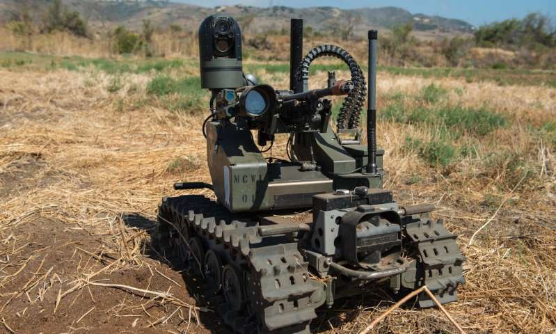
The U.S. military is already testing a Modular Advanced Armed Robotic System. Credit: Lance Cpl. Julien Rodarte, U.S. Marine Corps

That is a robot.

For the purposes of this posting, a robot is a piece of hardware which may or may not include an AI system and does not mimic a human or other biological organism such that you might, under circumstances, mistake the robot for a biological organism.

As for what precipitated this feature (in part), it seems there’s been a United Nations meeting in Geneva, Switzerland held from August 27 – 31, 2018 about war and the use of autonomous robots, i.e., robots equipped with AI systems and designed for independent action. BTW, it’s the not first meeting the UN has held on this topic.

Bonnie Docherty, lecturer on law and associate director of armed conflict and civilian protection, international human rights clinic, Harvard Law School, has written an August 21, 2018 essay on The Conversation (also on phys.org) describing the history and the current rules around the conduct of war, as well as, outlining the issues with the military use of autonomous robots (Note: Links have been removed),

When drafting a treaty on the laws of war at the end of the 19th century, diplomats could not foresee the future of weapons development. But they did adopt a legal and moral standard for judging new technology not covered by existing treaty language.

This standard, known as the Martens Clause, has survived generations of international humanitarian law and gained renewed relevance in a world where autonomous weapons are on the brink of making their own determinations about whom to shoot and when. The Martens Clause calls on countries not to use weapons that depart “from the principles of humanity and from the dictates of public conscience.”

I was the lead author of a new report by Human Rights Watch and the Harvard Law School International Human Rights Clinic that explains why fully autonomous weapons would run counter to the principles of humanity and the dictates of public conscience. We found that to comply with the Martens Clause, countries should adopt a treaty banning the development, production and use of these weapons.

Representatives of more than 70 nations will gather from August 27 to 31 [2018] at the United Nations in Geneva to debate how to address the problems with what they call lethal autonomous weapon systems. These countries, which are parties to the Convention on Conventional Weapons, have discussed the issue for five years. My co-authors and I believe it is time they took action and agreed to start negotiating a ban next year.

Docherty elaborates on her points (Note: A link has been removed),

The Martens Clause provides a baseline of protection for civilians and soldiers in the absence of specific treaty law. The clause also sets out a standard for evaluating new situations and technologies that were not previously envisioned.

Fully autonomous weapons, sometimes called “killer robots,” would select and engage targets without meaningful human control. They would be a dangerous step beyond current armed drones because there would be no human in the loop to determine when to fire and at what target. Although fully autonomous weapons do not yet exist, China, Israel, Russia, South Korea, the United Kingdom and the United States are all working to develop them. They argue that the technology would process information faster and keep soldiers off the battlefield.

The possibility that fully autonomous weapons could soon become a reality makes it imperative for those and other countries to apply the Martens Clause and assess whether the technology would offend basic humanity and the public conscience. Our analysis finds that fully autonomous weapons would fail the test on both counts.

I encourage you to read the essay in its entirety and for anyone who thinks the discussion about ethics and killer ‘bots is new or limited to military use, there’s my July 25, 2016 posting about police use of a robot in Dallas, Texas. (I imagine the discussion predates 2016 but that’s the earliest instance I have here.)

Teacher bots

Robots come in many forms and this one is on the humanoid end of the spectum,

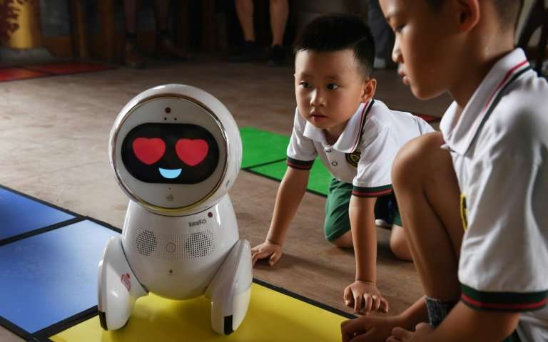
Children watch a Keeko robot at the Yiswind Institute of Multicultural Education in Beijing, where the intelligent machines are telling stories and challenging kids with logic problems  [donwloaded from https://phys.org/news/2018-08-robot-teachers-invade-chinese-kindergartens.html]

Don’t those ‘eyes’ look almost heart-shaped? No wonder the kids love these robots, if an August  29, 2018 news item on phys.org can be believed,

The Chinese kindergarten children giggled as they worked to solve puzzles assigned by their new teaching assistant: a roundish, short educator with a screen for a face.

Just under 60 centimetres (two feet) high, the autonomous robot named Keeko has been a hit in several kindergartens, telling stories and challenging children with logic problems.

Round and white with a tubby body, the armless robot zips around on tiny wheels, its inbuilt cameras doubling up both as navigational sensors and a front-facing camera allowing users to record video journals.

In China, robots are being developed to deliver groceries, provide companionship to the elderly, dispense legal advice and now, as Keeko’s creators hope, join the ranks of educators.

At the Yiswind Institute of Multicultural Education on the outskirts of Beijing, the children have been tasked to help a prince find his way through a desert—by putting together square mats that represent a path taken by the robot—part storytelling and part problem-solving.

Each time they get an answer right, the device reacts with delight, its face flashing heart-shaped eyes.

“Education today is no longer a one-way street, where the teacher teaches and students just learn,” said Candy Xiong, a teacher trained in early childhood education who now works with Keeko Robot Xiamen Technology as a trainer.

“When children see Keeko with its round head and body, it looks adorable and children love it. So when they see Keeko, they almost instantly take to it,” she added.

Keeko robots have entered more than 600 kindergartens across the country with its makers hoping to expand into Greater China and Southeast Asia.

Beijing has invested money and manpower in developing artificial intelligence as part of its “Made in China 2025” plan, with a Chinese firm last year unveiling the country’s first human-like robot that can hold simple conversations and make facial expressions.

According to the International Federation of Robots, China has the world’s top industrial robot stock, with some 340,000 units in factories across the country engaged in manufacturing and the automotive industry.

Moving on from hardware/software to a software only story.

AI fashion designer better than Balenciaga?

Despite the title for Katharine Schwab’s August 22, 2018 article for Fast Company, I don’t think this AI designer is better than Balenciaga but from the pictures I’ve seen the designs are as good and it does present some intriguing possibilities courtesy of its neural network (Note: Links have been removed),

The AI, created by researcher Robbie Barat, has created an entire collection based on Balenciaga’s previous styles. There’s a fabulous pink and red gradient jumpsuit that wraps all the way around the model’s feet–like a onesie for fashionistas–paired with a dark slouchy coat. There’s a textural color-blocked dress, paired with aqua-green tights. And for menswear, there’s a multi-colored, shimmery button-up with skinny jeans and mismatched shoes. None of these looks would be out of place on the runway.

To create the styles, Barat collected images of Balenciaga’s designs via the designer’s lookbooks, ad campaigns, runway shows, and online catalog over the last two months, and then used them to train the pix2pix neural net. While some of the images closely resemble humans wearing fashionable clothes, many others are a bit off–some models are missing distinct limbs, and don’t get me started on how creepy [emphasis mine] their faces are. Even if the outfits aren’t quite ready to be fabricated, Barat thinks that designers could potentially use a tool like this to find inspiration. Because it’s not constrained by human taste, style, and history, the AI comes up with designs that may never occur to a person. “I love how the network doesn’t really understand or care about symmetry,” Barat writes on Twitter.

You can see the ‘creepy’ faces and some of the designs here,

Image: Robbie Barat

In contrast to the previous two stories, this all about algorithms, no machinery with independent movement (robot hardware) needed.

Conversational android: Erica

Hiroshi Ishiguro and his lifelike (definitely humanoid) robots have featured here many, many times before. The most recent posting is a March 27, 2017 posting about his and his android’s participation at the 2017 SXSW festival.

His latest work is featured in an August 21, 2018 news news item on ScienceDaily,

We’ve all tried talking with devices, and in some cases they talk back. But, it’s a far cry from having a conversation with a real person.

Now a research team from Kyoto University, Osaka University, and the Advanced Telecommunications Research Institute, or ATR, have significantly upgraded the interaction system for conversational android ERICA, giving her even greater dialog skills.

ERICA is an android created by Hiroshi Ishiguro of Osaka University and ATR, specifically designed for natural conversation through incorporation of human-like facial expressions and gestures. The research team demonstrated the updates during a symposium at the National Museum of Emerging Science in Tokyo.

Here’s the latest conversational android, Erica

Caption: The experimental set up when the subject (left) talks with ERICA (right) Credit: Kyoto University / Kawahara lab

An August 20, 2018 Kyoto University press release on EurekAlert, which originated the news item, offers more details,

When we talk to one another, it’s never a simple back and forward progression of information,” states Tatsuya Kawahara of Kyoto University’s Graduate School of Informatics, and an expert in speech and audio processing.

“Listening is active. We express agreement by nodding or saying ‘uh-huh’ to maintain the momentum of conversation. This is called ‘backchanneling’, and is something we wanted to implement with ERICA.”

The team also focused on developing a system for ‘attentive listening’. This is when a listener asks elaborating questions, or repeats the last word of the speaker’s sentence, allowing for more engaging dialogue.

Deploying a series of distance sensors, facial recognition cameras, and microphone arrays, the team began collecting data on parameters necessary for a fluid dialog between ERICA and a human subject.

“We looked at three qualities when studying backchanneling,” continues Kawahara. “These were: timing — when a response happens; lexical form — what is being said; and prosody, or how the response happens.”

Responses were generated through machine learning using a counseling dialogue corpus, resulting in dramatically improved dialog engagement. Testing in five-minute sessions with a human subject, ERICA demonstrated significantly more dynamic speaking skill, including the use of backchanneling, partial repeats, and statement assessments.

“Making a human-like conversational robot is a major challenge,” states Kawahara. “This project reveals how much complexity there is in listening, which we might consider mundane. We are getting closer to a day where a robot can pass a Total Turing Test.”

Erica seems to have been first introduced publicly in Spring 2017, from an April 2017 Erica: Man Made webpage on The Guardian website,

Erica is 23. She has a beautiful, neutral face and speaks with a synthesised voice. She has a degree of autonomy – but can’t move her hands yet. Hiroshi Ishiguro is her ‘father’ and the bad boy of Japanese robotics. Together they will redefine what it means to be human and reveal that the future is closer than we might think.

Hiroshi Ishiguro and his colleague Dylan Glas are interested in what makes a human. Erica is their latest creation – a semi-autonomous android, the product of the most funded scientific project in Japan. But these men regard themselves as artists more than scientists, and the Erica project – the result of a collaboration between Osaka and Kyoto universities and the Advanced Telecommunications Research Institute International – is a philosophical one as much as technological one.

Erica is interviewed about her hope and dreams – to be able to leave her room and to be able to move her arms and legs. She likes to chat with visitors and has one of the most advanced speech synthesis systems yet developed. Can she be regarded as being alive or as a comparable being to ourselves? Will she help us to understand ourselves and our interactions as humans better?

Erica and her creators are interviewed in the science fiction atmosphere of Ishiguro’s laboratory, and this film asks how we might form close relationships with robots in the future. Ishiguro thinks that for Japanese people especially, everything has a soul, whether human or not. If we don’t understand how human hearts, minds and personalities work, can we truly claim that humans have authenticity that machines don’t?

Ishiguro and Glas want to release Erica and her fellow robots into human society. Soon, Erica may be an essential part of our everyday life, as one of the new children of humanity.

Key credits

  • Director/Editor: Ilinca Calugareanu
  • Producer: Mara Adina
  • Executive producers for the Guardian: Charlie Phillips and Laurence Topham
  • This video is produced in collaboration with the Sundance Institute Short Documentary Fund supported by the John D and Catherine T MacArthur Foundation

You can also view the 14 min. film here.

Artworks generated by an AI system are to be sold at Christie’s auction house

KC Ifeanyi’s August 22, 2018 article for Fast Company may send a chill down some artists’ spines,

For the first time in its 252-year history, Christie’s will auction artwork generated by artificial intelligence.

Created by the French art collective Obvious, “Portrait of Edmond de Belamy” is part of a series of paintings of the fictional Belamy family that was created using a two-part algorithm. …

The portrait is estimated to sell anywhere between $7,000-$10,000, and Obvious says the proceeds will go toward furthering its algorithm.

… Famed collector Nicolas Laugero-Lasserre bought one of Obvious’s Belamy works in February, which could’ve been written off as a novel purchase where the story behind it is worth more than the piece itself. However, with validation from a storied auction house like Christie’s, AI art could shake the contemporary art scene.

“Edmond de Belamy” goes up for auction from October 23-25 [2018].

Jobs safe from automation? Are there any?

Michael Grothaus expresses more optimism about future job markets than I’m feeling in an August 30, 2018 article for Fast Company,

A 2017 McKinsey Global Institute study of 800 occupations across 46 countries found that by 2030, 800 million people will lose their jobs to automation. That’s one-fifth of the global workforce. A further one-third of the global workforce will need to retrain if they want to keep their current jobs as well. And looking at the effects of automation on American jobs alone, researchers from Oxford University found that “47 percent of U.S. workers have a high probability of seeing their jobs automated over the next 20 years.”

The good news is that while the above stats are rightly cause for concern, they also reveal that 53% of American jobs and four-fifths of global jobs are unlikely to be affected by advances in artificial intelligence and robotics. But just what are those fields? I spoke to three experts in artificial intelligence, robotics, and human productivity to get their automation-proof career advice.

Creatives

“Although I believe every single job can, and will, benefit from a level of AI or robotic influence, there are some roles that, in my view, will never be replaced by technology,” says Tom Pickersgill, …

Maintenance foreman

When running a production line, problems and bottlenecks are inevitable–and usually that’s a bad thing. But in this case, those unavoidable issues will save human jobs because their solutions will require human ingenuity, says Mark Williams, head of product at People First, …

Hairdressers

Mat Hunter, director of the Central Research Laboratory, a tech-focused co-working space and accelerator for tech startups, have seen startups trying to create all kinds of new technologies, which has given him insight into just what machines can and can’t pull off. It’s lead him to believe that jobs like the humble hairdresser are safer from automation than those of, says, accountancy.

Therapists and social workers

Another automation-proof career is likely to be one involved in helping people heal the mind, says Pickersgill. “People visit therapists because there is a need for emotional support and guidance. This can only be provided through real human interaction–by someone who can empathize and understand, and who can offer advice based on shared experiences, rather than just data-driven logic.”

Teachers

Teachers are so often the unsung heroes of our society. They are overworked and underpaid–yet charged with one of the most important tasks anyone can have: nurturing the growth of young people. The good news for teachers is that their jobs won’t be going anywhere.

Healthcare workers

Doctors and nurses will also likely never see their jobs taken by automation, says Williams. While automation will no doubt better enhance the treatments provided by doctors and nurses the fact of the matter is that robots aren’t going to outdo healthcare workers’ ability to connect with patients and make them feel understood the way a human can.

Caretakers

While humans might be fine with robots flipping their burgers and artificial intelligence managing their finances, being comfortable with a robot nannying your children or looking after your elderly mother is a much bigger ask. And that’s to say nothing of the fact that even today’s most advanced robots don’t have the physical dexterity to perform the movements and actions carers do every day.

Grothaus does offer a proviso in his conclusion: certain types of jobs are relatively safe until developers learn to replicate qualities such as empathy in robots/AI.

It’s very confusing

There’s so much news about robots, artificial intelligence, androids, and cyborgs that it’s hard to keep up with it let alone attempt to get a feeling for where all this might be headed. When you add the fact that the term robots/artificial inteligence are often used interchangeably and that the distinction between robots/androids/cyborgs is not always clear any attempts to peer into the future become even more challenging.

At this point I content myself with tracking the situation and finding definitions so I can better understand what I’m tracking. Carmen Wong’s August 23, 2018 posting on the Signals blog published by Canada’s Centre for Commercialization of Regenerative Medicine (CCRM) offers some useful definitions in the context of an article about the use of artificial intelligence in the life sciences, particularly in Canada (Note: Links have been removed),

Artificial intelligence (AI). Machine learning. To most people, these are just buzzwords and synonymous. Whether or not we fully understand what both are, they are slowly integrating into our everyday lives. Virtual assistants such as Siri? AI is at work. The personalized ads you see when you are browsing on the web or movie recommendations provided on Netflix? Thank AI for that too.

AI is defined as machines having intelligence that imitates human behaviour such as learning, planning and problem solving. A process used to achieve AI is called machine learning, where a computer uses lots of data to “train” or “teach” itself, without human intervention, to accomplish a pre-determined task. Essentially, the computer keeps on modifying its algorithm based on the information provided to get to the desired goal.

Another term you may have heard of is deep learning. Deep learning is a particular type of machine learning where algorithms are set up like the structure and function of human brains. It is similar to a network of brain cells interconnecting with each other.

Toronto has seen its fair share of media-worthy AI activity. The Government of Canada, Government of Ontario, industry and multiple universities came together in March 2018 to launch the Vector Institute, with the goal of using AI to promote economic growth and improve the lives of Canadians. In May, Samsung opened its AI Centre in the MaRS Discovery District, joining a network of Samsung centres located in California, United Kingdom and Russia.

There has been a boom in AI companies over the past few years, which span a variety of industries. This year’s ranking of the top 100 most promising private AI companies covers 25 fields with cybersecurity, enterprise and robotics being the hot focus areas.

Wong goes on to explore AI deployment in the life sciences and concludes that human scientists and doctors will still be needed although she does note this in closing (Note: A link has been removed),

More importantly, empathy and support from a fellow human being could never be fully replaced by a machine (could it?), but maybe this will change in the future. We will just have to wait and see.

Artificial empathy is the term used in Lisa Morgan’s April 25, 2018 article for Information Week which unfortunately does not include any links to actual projects or researchers working on artificial empathy. Instead, the article is focused on how business interests and marketers would like to see it employed. FWIW, I have found a few references: (1) Artificial empathy Wikipedia essay (look for the references at the end of the essay for more) and (2) this open access article: Towards Artificial Empathy; How Can Artificial Empathy Follow the Developmental Pathway of Natural Empathy? by Minoru Asada.

Please let me know in the comments if you should have an insights on the matter in the comments section of this blog.

Humans can distinguish molecular differences by touch

Yesterday, in my December 18, 2017 post about medieval textiles, I posed the question, “How did medieval artisans create nanoscale and microscale gilding when they couldn’t see it?” I realized afterwards that an answer to that question might be in this December 13, 2017 news item on ScienceDaily,

How sensitive is the human sense of touch? Sensitive enough to feel the difference between surfaces that differ by just a single layer of molecules, a team of researchers at the University of California San Diego has shown.

“This is the greatest tactile sensitivity that has ever been shown in humans,” said Darren Lipomi, a professor of nanoengineering and member of the Center for Wearable Sensors at the UC San Diego Jacobs School of Engineering, who led the interdisciplinary project with V. S. Ramachandran, director of the Center for Brain and Cognition and distinguished professor in the Department of Psychology at UC San Diego.

So perhaps those medieval artisans were able to feel the difference before it could be seen in the textiles they were producing?

Getting back to the matter at hand, a December 13, 2017 University of California at San Diego (UCSD) news release (also on EurekAlert) by Liezel Labios offers more detail about the work,

Humans can easily feel the difference between many everyday surfaces such as glass, metal, wood and plastic. That’s because these surfaces have different textures or draw heat away from the finger at different rates. But UC San Diego researchers wondered, if they kept all these large-scale effects equal and changed only the topmost layer of molecules, could humans still detect the difference using their sense of touch? And if so, how?

Researchers say this fundamental knowledge will be useful for developing electronic skin, prosthetics that can feel, advanced haptic technology for virtual and augmented reality and more.

Unsophisticated haptic technologies exist in the form of rumble packs in video game controllers or smartphones that shake, Lipomi added. “But reproducing realistic tactile sensations is difficult because we don’t yet fully understand the basic ways in which materials interact with the sense of touch.”

“Today’s technologies allow us to see and hear what’s happening, but we can’t feel it,” said Cody Carpenter, a nanoengineering Ph.D. student at UC San Diego and co-first author of the study. “We have state-of-the-art speakers, phones and high-resolution screens that are visually and aurally engaging, but what’s missing is the sense of touch. Adding that ingredient is a driving force behind this work.”

This study is the first to combine materials science and psychophysics to understand how humans perceive touch. “Receptors processing sensations from our skin are phylogenetically the most ancient, but far from being primitive they have had time to evolve extraordinarily subtle strategies for discerning surfaces—whether a lover’s caress or a tickle or the raw tactile feel of metal, wood, paper, etc. This study is one of the first to demonstrate the range of sophistication and exquisite sensitivity of tactile sensations. It paves the way, perhaps, for a whole new approach to tactile psychophysics,” Ramachandran said.

Super-Sensitive Touch

In a paper published in Materials Horizons, UC San Diego researchers tested whether human subjects could distinguish—by dragging or tapping a finger across the surface—between smooth silicon wafers that differed only in their single topmost layer of molecules. One surface was a single oxidized layer made mostly of oxygen atoms. The other was a single Teflon-like layer made of fluorine and carbon atoms. Both surfaces looked identical and felt similar enough that some subjects could not differentiate between them at all.

According to the researchers, human subjects can feel these differences because of a phenomenon known as stick-slip friction, which is the jerking motion that occurs when two objects at rest start to slide against each other. This phenomenon is responsible for the musical notes played by running a wet finger along the rim of a wine glass, the sound of a squeaky door hinge or the noise of a stopping train. In this case, each surface has a different stick-slip frequency due to the identity of the molecules in the topmost layer.

In one test, 15 subjects were tasked with feeling three surfaces and identifying the one surface that differed from the other two. Subjects correctly identified the differences 71 percent of the time.

In another test, subjects were given three different strips of silicon wafer, each strip containing a different sequence of 8 patches of oxidized and Teflon-like surfaces. Each sequence represented an 8-digit string of 0s and 1s, which encoded for a particular letter in the ASCII alphabet. Subjects were asked to “read” these sequences by dragging a finger from one end of the strip to the other and noting which patches in the sequence were the oxidized surfaces and which were the Teflon-like surfaces. In this experiment, 10 out of 11 subjects decoded the bits needed to spell the word “Lab” (with the correct upper and lowercase letters) more than 50 percent of the time. Subjects spent an average of 4.5 minutes to decode each letter.

“A human may be slower than a nanobit per second in terms of reading digital information, but this experiment shows a potentially neat way to do chemical communications using our sense of touch instead of sight,” Lipomi said.

Basic Model of Touch

The researchers also found that these surfaces can be differentiated depending on how fast the finger drags and how much force it applies across the surface. The researchers modeled the touch experiments using a “mock finger,” a finger-like device made of an organic polymer that’s connected by a spring to a force sensor. The mock finger was dragged across the different surfaces using multiple combinations of force and swiping velocity. The researchers plotted the data and found that the surfaces could be distinguished given certain combinations of velocity and force. Meanwhile, other combinations made the surfaces indistinguishable from each other.

“Our results reveal a remarkable human ability to quickly home in on the right combinations of forces and swiping velocities required to feel the difference between these surfaces. They don’t need to reconstruct an entire matrix of data points one by one as we did in our experiments,” Lipomi said.

“It’s also interesting that the mock finger device, which doesn’t have anything resembling the hundreds of nerves in our skin, has just one force sensor and is still able to get the information needed to feel the difference in these surfaces. This tells us it’s not just the mechanoreceptors in the skin, but receptors in the ligaments, knuckles, wrist, elbow and shoulder that could be enabling humans to sense minute differences using touch,” he added.

This work was supported by member companies of the Center for Wearable Sensors at UC San Diego: Samsung, Dexcom, Sabic, Cubic, Qualcomm and Honda.

For those who prefer their news by video,

Here’s a link to and a citation for the paper,

Human ability to discriminate surface chemistry by touch by Cody W. Carpenter, Charles Dhong, Nicholas B. Root, Daniel Rodriquez, Emily E. Abdo, Kyle Skelil, Mohammad A. Alkhadra, Julian Ramírez, Vilayanur S. Ramachandran and Darren J. Lipomi. Mater. Horiz., 2018, Advance Article DOI: 10.1039/C7MH00800G

This paper is open access but you do need to have opened a free account on the website.

IBM and a 5 nanometre chip

If this continues, they’re going to have change the scale from nano to pico. IBM has announced work on a 5 nanometre (5nm) chip in a June 5, 2017 news item on Nanotechnology Now,

IBM (NYSE: IBM), its Research Alliance partners GLOBALFOUNDRIES and Samsung, and equipment suppliers have developed an industry-first process to build silicon nanosheet transistors that will enable 5 nanometer (nm) chips. The details of the process will be presented at the 2017 Symposia on VLSI Technology and Circuits conference in Kyoto, Japan. In less than two years since developing a 7nm test node chip with 20 billion transistors, scientists have paved the way for 30 billion switches on a fingernail-sized chip.

A June 5, 2017 IBM news release, which originated the news item, spells out some of the details about IBM’s latest breakthrough,

The resulting increase in performance will help accelerate cognitive computing [emphasis mine], the Internet of Things (IoT), and other data-intensive applications delivered in the cloud. The power savings could also mean that the batteries in smartphones and other mobile products could last two to three times longer than today’s devices, before needing to be charged.

Scientists working as part of the IBM-led Research Alliance at the SUNY Polytechnic Institute Colleges of Nanoscale Science and Engineering’s NanoTech Complex in Albany, NY achieved the breakthrough by using stacks of silicon nanosheets as the device structure of the transistor, instead of the standard FinFET architecture, which is the blueprint for the semiconductor industry up through 7nm node technology.

“For business and society to meet the demands of cognitive and cloud computing in the coming years, advancement in semiconductor technology is essential,” said Arvind Krishna, senior vice president, Hybrid Cloud, and director, IBM Research. “That’s why IBM aggressively pursues new and different architectures and materials that push the limits of this industry, and brings them to market in technologies like mainframes and our cognitive systems.”

The silicon nanosheet transistor demonstration, as detailed in the Research Alliance paper Stacked Nanosheet Gate-All-Around Transistor to Enable Scaling Beyond FinFET, and published by VLSI, proves that 5nm chips are possible, more powerful, and not too far off in the future.

Compared to the leading edge 10nm technology available in the market, a nanosheet-based 5nm technology can deliver 40 percent performance enhancement at fixed power, or 75 percent power savings at matched performance. This improvement enables a significant boost to meeting the future demands of artificial intelligence (AI) systems, virtual reality and mobile devices.

Building a New Switch

“This announcement is the latest example of the world-class research that continues to emerge from our groundbreaking public-private partnership in New York,” said Gary Patton, CTO and Head of Worldwide R&D at GLOBALFOUNDRIES. “As we make progress toward commercializing 7nm in 2018 at our Fab 8 manufacturing facility, we are actively pursuing next-generation technologies at 5nm and beyond to maintain technology leadership and enable our customers to produce a smaller, faster, and more cost efficient generation of semiconductors.”

IBM Research has explored nanosheet semiconductor technology for more than 10 years. This work is the first in the industry to demonstrate the feasibility to design and fabricate stacked nanosheet devices with electrical properties superior to FinFET architecture.

This same Extreme Ultraviolet (EUV) lithography approach used to produce the 7nm test node and its 20 billion transistors was applied to the nanosheet transistor architecture. Using EUV lithography, the width of the nanosheets can be adjusted continuously, all within a single manufacturing process or chip design. This adjustability permits the fine-tuning of performance and power for specific circuits – something not possible with today’s FinFET transistor architecture production, which is limited by its current-carrying fin height. Therefore, while FinFET chips can scale to 5nm, simply reducing the amount of space between fins does not provide increased current flow for additional performance.

“Today’s announcement continues the public-private model collaboration with IBM that is energizing SUNY-Polytechnic’s, Albany’s, and New York State’s leadership and innovation in developing next generation technologies,” said Dr. Bahgat Sammakia, Interim President, SUNY Polytechnic Institute. “We believe that enabling the first 5nm transistor is a significant milestone for the entire semiconductor industry as we continue to push beyond the limitations of our current capabilities. SUNY Poly’s partnership with IBM and Empire State Development is a perfect example of how Industry, Government and Academia can successfully collaborate and have a broad and positive impact on society.”

Part of IBM’s $3 billion, five-year investment in chip R&D (announced in 2014), the proof of nanosheet architecture scaling to a 5nm node continues IBM’s legacy of historic contributions to silicon and semiconductor innovation. They include the invention or first implementation of the single cell DRAM, the Dennard Scaling Laws, chemically amplified photoresists, copper interconnect wiring, Silicon on Insulator, strained engineering, multi core microprocessors, immersion lithography, high speed SiGe, High-k gate dielectrics, embedded DRAM, 3D chip stacking and Air gap insulators.

I last wrote about IBM and computer chips in a July 15, 2015 posting regarding their 7nm chip. You may want to scroll down approximately 55% of the way where I note research from MIT (Massachusetts Institute of Technology) about metal nanoparticles with unexpected properties possibly having an impact on nanoelectronics.

Getting back to IBM, they have produced a slick video about their 5nm chip breakthrough,

Meanwhile, Katherine Bourzac provides technical detail in a June 5, 2017 posting on the Nanoclast blog (on the IEEE [Institute of Electrical and Electronics Engineers] website), Note: A link has been removed,

Researchers at IBM believe the future of the transistor is in stacked nanosheets. …

Today’s state-of-the-art transistor is the finFET, named for the fin-like ridges of current-carrying silicon that project from the chip’s surface. The silicon fins are surrounded on their three exposed sides by a structure called the gate. The gate switches the flow of current on, and prevents electrons from leaking out when the transistor is off. This design is expected to last from this year’s bleeding-edge process technology, the “10-nanometer” node, through the next node, 7 nanometers. But any smaller, and these transistors will become difficult to switch off: electrons will leak out, even with the three-sided gates.

So the semiconductor industry has been working on alternatives for the upcoming 5 nanometer node. One popular idea is to use lateral silicon nanowires that are completely surrounded by the gate, preventing electron leaks and saving power. This design is called “gate all around.” IBM’s new design is a variation on this. In their test chips, each transistor is made up of three stacked horizontal sheets of silicon, each only a few nanometers thick and completely surrounded by a gate.

Why a sheet instead of a wire? Huiming Bu, director of silicon integration and devices at IBM, says nanosheets can bring back one of the benefits of pre-finFET, planar designs. Designers used to be able to vary the width of a transistor to prioritize fast operations or energy efficiency. Varying the amount of silicon in a finFET transistor is not practicable because it would mean making some fins taller and other shorter. Fins must all be the same height due to manufacturing constraints, says Bu.

IBM’s nanosheets can range from 8 to 50 nanometers in width. “Wider gives you better performance but takes more power, smaller width relaxes performance but reduces power use,” says Bu. This will allow circuit designers to pick and choose what they need, whether they are making a power efficient mobile chip processor or designing a bank of SRAM memory. “We are bringing flexibility back to the designers,” he says.

The test chips have 30 billion transistors. …

It was a struggle trying to edit Bourzac’s posting with its good detail and clear writing. I encourage you to read it (June 5, 2017 posting) in its entirety.

As for where this drive downwards to the ‘ever smaller’ is going, there’s Dexter’s Johnson’s June 29, 2017 posting about another IBM team’s research on his Nanoclast blog on the IEEE website (Note: Links have been removed),

There have been increasing signs coming from the research community that carbon nanotubes are beginning to step up to the challenge of offering a real alternative to silicon-based complementary metal-oxide semiconductor (CMOS) transistors.

Now, researchers at IBM Thomas J. Watson Research Center have advanced carbon nanotube-based transistors another step toward meeting the demands of the International Technology Roadmap for Semiconductors (ITRS) for the next decade. The IBM researchers have fabricated a p-channel transistor based on carbon nanotubes that takes up less than half the space of leading silicon technologies while operating at a lower voltage.

In research described in the journal Science, the IBM scientists used a carbon nanotube p-channel to reduce the transistor footprint; their transistor contains all components to 40 square nanometers [emphasis mine], an ITRS roadmap benchmark for ten years out.

One of the keys to being able to reduce the transistor to such a small size is the use of the carbon nanotube as the channel in place of silicon. The nanotube is only 1 nanometer thick. Such thinness offers a significant advantage in electrostatics, so that it’s possible to reduce the device gate length to 10 nanometers without seeing the device performance adversely affected by short-channel effects. An additional benefit of the nanotubes is that the electrons travel much faster, which contributes to a higher level of device performance.

Happy reading!

Nanotech business news from Turkey and from Northern Ireland

I have two nanotech business news bits, one from Turkey and one from Northern Ireland.

Turkey

A Turkish company has sold one of its microscopes to the US National Aeronautics and Space Administration (NASA), according to a Jan. 20, 2017 news item on dailysabah.com,

Turkish nanotechnology company Nanomanyetik has begun selling a powerful microscope to the U.S. space agency NASA, the company’s general director told Anadolu Agency on Thursday [Jan. 19, 2017].

Dr. Ahmet Oral, who also teaches physics at Middle East Technical University, said Nanomanyetik developed a microscope that is able to map surfaces on the nanometric and atomic levels, or extremely small particles.

Nanomanyetik’s foreign customers are drawn to the microscope because of its higher quality yet cheaper price compared to its competitors.

“There are almost 30 firms doing this work,” according to Oral. “Ten of them are active and we are among these active firms. Our aim is to be in the top three,” he said, adding that Nanomanyetik jumps to the head of the line because of its after-sell service.

In addition to sales to NASA, the Ankara-based firm exports the microscope to Brazil, Chile, France, Iran, Israel, Italy, Japan, Poland, South Korea and Spain.

Electronics giant Samsung is also a customer.

“Where does Samsung use this product? There are pixels in the smartphones’ displays. These pixels are getting smaller each year. Now the smallest pixel is 15X10 microns,” he said. Human hair is between 10 and 100 microns in diameter.

“They are figuring inner sides of pixels so that these pixels can operate much better. These patterns are on the nanometer level. They are using these microscopes to see the results of their works,” Oral said.

Nanomanyetik’s microscopes produces good quality, high resolution images and can even display an object’s atoms and individual DNA fibers, according to Oral.

You can find the English language version of the Nanomanyetik (NanoMagnetics Instruments) website here . For those with the language skills there is the Turkish language version, here.

Northern Ireland

A Jan. 22, 2017 news article by Dominic Coyle for The Irish Times (Note: Links have been removed) shares this business news and mention of a world first,

MOF Technologies has raised £1.5 million (€1.73 million) from London-based venture capital group Excelsa Ventures and Queen’s University Belfast’s Qubis research commercialisation group.

MOF Technologies chief executive Paschal McCloskey welcomed the Excelsa investment.

Established in part by Qubis in 2012 in partnership with inventor Prof Stuart James, MOF Technologies began life in a lab at the School of Chemistry and Chemical Engineering at Queen’s.

Its metal organic framework (MOF) technology is seen as having significant potential in areas including gas storage, carbon capture, transport, drug delivery and heat transformation. Though still in its infancy, the market is forecast to grow to £2.2 billion by 2022, the company says.

MOF Technologies last year became the first company worldwide to successfully commercialise MOFs when it agreed a deal with US fruit and vegetable storage provider Decco Worldwide to commercialise MOFs for use in a food application.

TruPick, designed by Decco and using MOF Technologies’ environmentally friendly technology, enables nanomaterials control the effects of ethylene on fruit produce so it maintains freshness in storage or transport.

MOFs are crystalline, sponge-like materials composed of two components – metal ions and organic molecules known as linkers.

“We very quickly recognised the market potential of MOFs in terms of their unmatched ability for gas storage,” said Moritz Bolle from Excelsa Ventures. “This technology will revolutionise traditional applications and open countless new opportunities for industry. We are confident MOF Technologies is the company that will lead this seismic shift in materials science.

You can find MOF Technologies here.

Maths gallery at the UK’s Science Museum takes flight

Mathematics: The Winton Gallery at the Science Museum, Zaha Hadid Architects’ only permanent public museum exhibition design. London. Photograph: Nicholas Guttridge/NIck Guttridge

This exhibition looks great in the picture, I wonder what the experience is like. Alex Bellos is certainly enthusiastic in his Dec. 7, 2016 posting on the Guardian’s website,

Mathematics underlies all science, so for a science museum to be worthy of the name, maths needs to included somewhere. Yet maths, which deals mainly in abstract objects, is [a] challenge for museums, which necessarily contain physical ones. The Science Museum’s approach in its new gallery is to tell historical stories about the influence of mathematics in the real world, rather than actually focussing directly on the mathematical ideas involved. The result is a stunning gallery, with fascinating objects beautifully laid out, yet which eschews explaining any maths. (If you want to learn simple mathematical ideas, you can always head to the museum’s new interactive gallery, Wonderlab).

Much of the attention on Mathematics: The Winton Gallery – the main funders are David Harding, founder and CEO of investment firm Winton, and his wife Claudia – has been on Zaha Hadid’s design. The gallery is the first UK project by Zaha Hadid Architects to open since her unexpected death in March [2016], and the only permanent public museum exhibition she designed. Her first degree was in maths, before she turned to architecture.

Hanging from the ceiling is an aeroplane – the Handley Page ‘Gugnunc’, built in 1929 for a competition to build safe aircraft – and surrounding it is a swirly ceiling sculpture that represents the mathematical equations that describe airflow. In fact, the entire gallery follows the contours of the flow, providing the positions of the cabinets below.

The Science Museum’s previous maths gallery, which had not been updated in decades, contained about 600 objects, including cabinets crammed with geometrical objects and many examples of the same thing, such as medieval slide rules or Victorian curve-drawing machines. The new gallery has less than a quarter of that number of objects in the same space.

Every object now is in its own cabinet, and the extra space means you can walk around them from all angles, as well as making the gallery feel more manageable. Rather than being bombarded with stuff, you are given a single object to contemplate that tells part of a wider story.

In a section on “form and beauty”, there is a modern replica of a 1920s chair based on French architect’s Le Corbusier’s Modulor system of proportions, and two J W Turner sketches from his Royal Academy lectures on perspective.

The section “trade and travel” has a 3-metre long replica of the 1973 Globtik Tokyo oil tanker, then the largest ship in the world. In its massive cabinet it looks as terrifying as a Damien Hirst shark. The maths link? Because British mathematician William Froode a century before had worked out that bulbous bows were better than sharp bows at the fronts of boats and ships.

The new maths gallery is a wonderfully attractive space, full of interesting and thought-provoking objects, and a very welcome addition [geddit?] to London’s museums. Go!

A Dec. 8 (?), 2016 [London, UK] Science Museum press release is the first example I’ve seen of the funders being highlighted quite so prominently, i.e., before the press release proper,

Mathematics: The Winton Gallery designed by Zaha Hadid Architects opens at the Science Museum

  • A stunning new permanent gallery that reveals the importance of mathematics in all our lives through remarkable historical artefacts, stories and design
  • Free to visit and open daily from 8 December 2016
  • The only permanent public museum exhibition designed by Zaha Hadid anywhere in the world

Principal Funder: David and Claudia Harding
Principal Sponsor: Samsung
Major Sponsor: MathWorks

On 8 December 2016 the Science Museum will open an inspirational new mathematics gallery, designed by Zaha Hadid Architects.

Mathematics: The Winton Gallery brings together remarkable stories, historical artefacts and design to highlight the central role of mathematical practice in all our lives, and explores how mathematicians, their tools and ideas have helped build the modern world over the past four centuries.

More than 100 treasures from the Science Museum’s world-class science, technology, engineering and mathematics collections have been selected to tell powerful stories about how mathematics has shaped, and been shaped by, some of our most fundamental human concerns – from trade and travel to war, peace, life, death, form and beauty.

Curator Dr David Rooney said, ‘At its heart this gallery reveals a rich cultural story of human endeavour that has helped transform the world over the last four hundred years. Mathematical practice underpins so many aspects of our lives and work, and we hope that bringing together these remarkable stories, people and exhibits will inspire visitors to think about the role of mathematics in a new light.’

Positioned at the centre of the gallery is the Handley Page ‘Gugnunc’ aeroplane, built in 1929 for a competition to construct safe aircraft. Ground-breaking aerodynamic research influenced the wing design of this experimental aeroplane, helping to shift public opinion about the safety of flying and to secure the future of the aviation industry. This aeroplane encapsulates the gallery’s overarching theme, illustrating how mathematical practice has helped solve real-world problems and in this instance paved the way for the safe passenger flights that we rely on today.

Mathematics also defines Zaha Hadid Architects’ enlightening design for the gallery. Inspired by the Handley Page aircraft, the design is driven by equations of airflow used in the aviation industry. The layout and lines of the gallery represent the air that would have flowed around this historic aircraft in flight, from the positioning of the showcases and benches to the three-dimensional curved surfaces of the central pod structure.

Mathematics: The Winton Gallery is the first permanent public museum exhibition designed by Zaha Hadid Architects anywhere in the world. The gallery is also the first of Zaha Hadid Architects’ projects to open in the UK since Dame Zaha Hadid’s sudden death in March 2016. The late Dame Zaha first became interested in geometry while studying mathematics at university. Mathematics and geometry have a strong connection with architecture and she continued to examine these relationships throughout each of her projects; with mathematics always central to her work. As Dame Zaha said, ‘When I was growing up in Iraq, math was an everyday part of life. We would play with math problems just as we would play with pens and paper to draw – math was like sketching.’

Ian Blatchford, Director of the Science Museum Group, said, ‘We were hugely impressed by the ideas and vision of the late Dame Zaha Hadid and Patrik Schumacher when they first presented their design for the new mathematics gallery over two years ago. It was a terrible shock for us all when Dame Zaha died suddenly in March this year, but I am sure that this gallery will be a lasting tribute to this world-changing architect and provide inspiration for our millions of visitors for many years to come.’

From a beautiful 17th century Islamic astrolabe that uses ancient mathematical techniques to map the night sky, to an early example of the famous Enigma machine, designed to resist even the most advanced mathematical techniques for code breaking during the Second World War, each historic object within the gallery has an important story to tell. Archive photography and film helps to capture these stories, and introduces the wide range of people who made, used or were impacted by each mathematical device or idea.

Some instruments and objects within the gallery clearly reference their mathematical origin. Others may surprise visitors and appear rooted in other disciplines, from classical architecture to furniture design. Visitors will see a box of glass eyes used by Francis Galton in his 1884 Anthropometric Laboratory to help measure the physical characteristics of the British public and develop statistics to support a wider social and political movement he termed ‘eugenics’. On the other side of the gallery is the pioneering Wisard pattern-recognition machine built in 1981 to attempt to re-create the ‘neural networks’ of the brain. This early Artificial Intelligence machine worked, until 1995, on a variety of projects, from banknote recognition to voice analysis, and from foetal growth monitoring in hospitals to covert surveillance for the Home Office.

A richly illustrated book has been published by Scala to accompany the new gallery. Mathematics: How it Shaped Our World, written by David Rooney, expands on the themes and stories that are celebrated in the gallery itself and includes a series of newly commissioned essays written by world-leading experts in the history and modern practice of mathematics.

David Harding, Principal Funder of the gallery and Founder and CEO of Winton said, ‘Mathematics, whilst difficult for many, is incredibly useful. To those with an aptitude for it, it is also beautiful. I’m delighted that this gallery will be both useful and beautiful.’

Mathematics: The Winton Gallery is free to visit and open daily from 8 December 2016. The gallery has been made possible through an unprecedented donation from long-standing supporters of science, David and Claudia Harding. It has also received generous support from Samsung as Principal Sponsor, MathWorks as Major Sponsor, with additional support from Adrian and Jacqui Beecroft, Iain and Jane Bratchie, the Keniston-Cooper Charitable Trust, Dr Martin Schoernig, Steve Mobbs and Pauline Thomas.

After the press release, there is the most extensive list of ‘Abouts’ I’ve seen yet (Note: This includes links to the Science Museum and other agencies),

About the Science Museum
The Science Museum’s world-class collection forms an enduring record of scientific, technological and medical achievements from across the globe. Welcoming over 3 million visitors a year, the Museum aims to make sense of the science that shapes our lives, inspiring visitors with iconic objects, award-winning exhibitions and incredible stories of scientific achievement. More information can be found at sciencemuseum.org.uk

About Curator David Rooney
Mathematics: The Winton Gallery has been curated by Dr David Rooney, who was responsible for the award-winning 2012 Science Museum exhibition Codebreaker: Alan Turing’s Life and Legacy as well as developing galleries on time and navigation at the National Maritime Museum, Greenwich. David writes and speaks widely on the history of technology and engineering. His critically acclaimed first book, Ruth Belville: The Greenwich Time Lady, was described by Jonathan Meades as ‘an engrossing and eccentric slice of London history’, and by the Daily Telegraph as ‘a gem of a book’. He has recently authored Mathematics: How It Shaped Our World, to accompany the new mathematics gallery, and is currently writing a political history of traffic.

About David and Claudia Harding
David and Claudia Harding are associated with Winton, one of the world’s leading quantitative investment management firms which David founded in 1997. Winton uses mathematical and scientific methods to devise, evaluate and execute investment ideas on behalf of clients all over the world. A British-based company, Winton and David and Claudia Harding have donated to numerous scientific and mathematical causes in the UK and internationally, including Cambridge University, the Crick Institute, the Max Planck Institute, and the Science Museum. The main themes of their philanthropy have been supporting basic scientific research and the communication of scientific ideas. David and Claudia reside in London.

About Samsung’s Citizenship Programmes
Samsung is committed to help close the digital divide and skills gap in the UK. Samsung Digital Classrooms in schools, charities/non-profit organisations and cultural partners provide access to the latest technology. Samsung is also providing the training and maintenance support necessary to help make the transition and integration of the new technology as smooth as possible. Samsung also offers qualifications and training in technology for young people and teachers through its Digital Academies. These initiatives will inspire young people, staff and teachers to learn and teach in new exciting ways and to help encourage young people into careers using technology. Find out more

About MathWorks
MathWorks is the leading developer of mathematical computing software. MATLAB, the language of technical computing, is a programming environment for algorithm development, data analysis, visualisation, and numeric computation. Simulink is a graphical environment for simulation and Model-Based Design for multidomain dynamic and embedded systems. Engineers and scientists worldwide rely on these product families to accelerate the pace of discovery, innovation, and development in automotive, aerospace, electronics, financial services, biotech-pharmaceutical, and other industries. MATLAB and Simulink are also fundamental teaching and research tools in the world’s universities and learning institutions. Founded in 1984, MathWorks employs more than 3000 people in 15 countries, with headquarters in Natick, Massachusetts, USA. For additional information, visit mathworks.com

About Zaha Hadid Architects
Zaha Hadid founded Zaha Hadid Architects (ZHA) in 1979. Each of ZHA’s projects builds on over thirty years of exploration and research in the interrelated fields of urbanism, architecture and design. Hadid’s pioneering vision redefined architecture for the 21st century and captured imaginations across the globe. Her legacy is embedded within the DNA of the design studio she created as ZHA’s projects combine the unwavering belief in the power of invention with concepts of connectivity and fluidity.

ZHA is currently working on a diversity of projects worldwide including the new Beijing Airport Terminal Building in Daxing, China, the Sleuk Rith Institute in Phnom Penh, Cambodia and 520 West 28th Street in New York City, USA. The practice’s portfolio includes cultural, academic, sporting, residential, and transportation projects across six continents.

About Discover South Kensington
Discover South Kensington brings together the Science Museum and other leading cultural and educational organisations to promote innovation and learning. South Kensington is the home of science, arts and inspiration. Discovery is at the core of what happens here and there is so much to explore every day. discoversouthken.com

About Zaha Hadid: Early Paintings and Drawings at the Serpentine Sackler Gallery
This week an exhibition of paintings and drawings by Zaha Hadid will open at the Serpentine Galleries that will reveal her as an artist with drawing at the very heart of her work. It will include calligraphic drawings and rarely seen private notebooks, showing her complex thoughts about architecture’s forms and relationship to the world we live in. Zaha Hadid: Early Paintings and Drawings at the Serpentine Sackler Gallery is free to visit and runs from 8th December 2016 – 12th February 2017.

I found the mentions of Zaha Hadid fascinating and so I looked her up on Wikipedia, where I found this (Note: Links have been removed),

Dame Zaha Mohammad Hadid, DBE (Arabic: زها حديد‎‎ Zahā Ḥadīd; 31 October 1950 – 31 March 2016) was an Iraqi-born British architect. She was the first woman to receive the Pritzker Architecture Prize, in 2004.[1] She received the UK’s most prestigious architectural award, the Stirling Prize, in 2010 and 2011. In 2012, she was made a Dame by Elizabeth II for services to architecture, and in 2015 she became the first woman to be awarded the Royal Gold Medal from the Royal Institute of British Architects.[2]

She was dubbed by The Guardian as the ‘Queen of the curve’.[3] She liberated architectural geometry[4] with the creation of highly expressive, sweeping fluid forms of multiple perspective points and fragmented geometry that evoke the chaos and flux of modern life.[5] A pioneer of parametricism, and an icon of neo-futurism, with a formidable personality, her acclaimed work and ground-breaking forms include the aquatic centre for the London 2012 Olympics, the Broad Art Museum in the US, and the Guangzhou Opera House in China.[6] At the time of her death in 2016, Zaha Hadid Architects in London was the fastest growing British architectural firm.[7] Many of her designs are to be released posthumously, ranging in variation from the 2017 Brit Awards statuette to a 2022 FIFA World Cup stadium.[8][9]

Dubbed ‘Queen of the curve’, Hadid has a reputation as the world’s top female architect,[3][62][63][64][65] although her reputation is not without criticism. She is considered an architect of unconventional thinking, whose buildings are organic, dynamic and sculptural.[66][67] Stanton and others also compliment her on her unique organic designs: “One of the main characteristics of her work is that however clearly recognizable, it can never be pigeonholed into a stylistic signature. Digital knowledge, technology-driven mutations, shapes inspired by the organic and biological world, as well as geometrical interpretation of the landscape are constant elements of her practice. Yet, the multiplicity and variety of the combination among these facets prevent the risk of self-referential solutions and repetitions.”[68] Allison Lee Palmer considers Hadid a leader of Deconstructivism in architecture, writing that, “Almost all of Hadid’s buildings appear to melt, bend, and curve into a new architectural language that defies description. Her completed buildings span the globe and include the Jockey Club Innovation Tower on the north side of the Hong Kong Polytechnic University in Hong Kong, completed in 2013, that provides Hong Kong an entry into the world stage of cutting-edge architecture by revealing a design that dissolved traditional architecture, the so called modernist “glass box,” into a shattering of windows and melting of walls to form organic structures with halls and stairways that flow through the building, pooling open into rooms and foyers.”[69]

Hadid’s architectural language has been described by some as “famously extravagant” with many of her projects sponsored by “dictator states”. [emphasis mine] [70] Rowan Moore described Hadid’s Heydar Aliyev Center as “not so different from the colossal cultural palaces long beloved of Soviet and similar regimes”. Architect Sean Griffiths characterised Hadid’s work as “an empty vessel that sucks in whatever ideology might be in proximity to it”.[71] Art historian Maike Aden criticises in particular the foreclosure of Zaha Hadid’s architecture of the MAXXI in Rome towards the public and the urban life that undermines even the most impressive program to open the museum.[72]

If you think about it, most of the world’s great monuments were built by dictators or omnipotent rulers of one country or another. Getting the money and commitment can present an ethical/moral issue for any artist or architect who has a ‘grand design’.

Graphene Malaysia 2016 gathering and Malaysia’s National Graphene Action Plan 2020

Malaysia is getting ready to host a graphene conference according to an Oct. 10, 2016 news item on Nanotechnology Now,

The Graphene Malaysia 2016 [Nov. 8 – 9, 2016] (www.graphenemalaysiaconf.com) is jointly organized by NanoMalaysia Berhad and Phantoms Foundation. The conference will be centered on graphene industry interaction and collaborative innovation. The event will be launched under the National Graphene Action Plan 2020 (NGAP 2020), which will generate about 9,000 jobs and RM20 (US$4.86) billion GNI impact by the year 2020.

First speakers announced:
Murni Ali (Nanomalaysia, Malaysia) | Francesco Bonaccorso (Istituto Italiano di Tecnologia, Italy) | Antonio Castro Neto (NUS, Singapore) | Antonio Correia (Phantoms Foundation, Spain)| Pedro Gomez-Romero (ICN2 (CSIC-BIST), Spain) | Shu-Jen Han (Nanoscale Science & Technology IBM T.J. Watson Research Center, USA) | Kuan-Tsae Huang (AzTrong, USA/Taiwan) | Krzysztof Koziol (FGV Cambridge Nanosystems, UK) | Taavi Madiberk (Skeleton Technologies, Estonia) | Richard Mckie (BAE Systems, UK) | Pontus Nordin (Saab AB, Saab Aeronautics, Sweden) | Elena Polyakova (Graphene Laboratories Inc., USA) | Ahmad Khairuddin Abdul Rahim (Malaysian Investment Development Authority (MIDA), Malaysia) | Adisorn Tuantranont (Thailand Organic and Printed Electronics Innovation Center, Thailand) |Archana Venugopal (Texas Instruments, USA) | Won Jong Yoo (Samsung-SKKU Graphene-2D Center (SSGC), South Korea) | Hongwei Zhu (Tsinghua University, China)

You can check for more information and deadlines in the Nanotechnology Now Oct. 10, 2016 news item.

The Graphene Malalysia 2016 conference website can be found here and Malaysia’s National Graphene Action Plan 2020, which is well written, can be found here (PDF).  This portion from the executive summary offers some insight into Malyasia’s plans to launch itself into the world of high income nations,

Malaysia’s aspiration to become a high-income nation by 2020 with improved jobs and better outputs is driving the country’s shift away from “business as usual,” and towards more innovative and high value add products. Within this context, and in accordance with National policies and guidelines, Graphene, an emerging, highly versatile carbon-based nanomaterial, presents a unique opportunity for Malaysia to develop a high value economic ecosystem within its industries.  Isolated only in 2004, Graphene’s superior physical properties such as electrical/ thermal conductivity, high strength and high optical transparency, combined with its manufacturability have raised tremendous possibilities for its application across several functions and make it highly interesting for several applications and industries.  Currently, Graphene is still early in its development cycle, affording Malaysian companies time to develop their own applications instead of relying on international intellectual property and licenses.

Considering the potential, several leading countries are investing heavily in associated R&D. Approaches to Graphene research range from an expansive R&D focus (e.g., U.S. and the EU) to more focused approaches aimed at enhancing specific downstream applications with Graphene (e.g., South Korea). Faced with the need to push forward a multitude of development priorities, Malaysia must be targeted in its efforts to capture Graphene’s potential, both in terms of “how to compete” and “where to compete”. This National Graphene Action Plan 2020 lays out a set of priority applications that will be beneficial to the country as a whole and what the government will do to support these efforts.

Globally, much of the Graphene-related commercial innovation to date has been upstream, with producers developing techniques to manufacture Graphene at scale. There has also been some development in downstream sectors, as companies like Samsung, Bayer MaterialScience, BASF and Siemens explore product enhancement with Graphene in lithium-ion battery anodes and flexible displays, and specialty plastic and rubber composites. However the speed of development has been uneven, offering Malaysian industries willing to invest in innovation an opportunity to capture the value at stake. Since any innovation action plan has to be tailored to the needs and ambitions of local industry, Malaysia will focus its Graphene action plan initially on larger domestic industries (e.g., rubber) and areas already being targeted by the government for innovation such as energy storage for electric vehicles and conductive inks.

In addition to benefiting from the physical properties of Graphene, Malaysian downstream application providers may also capture the benefits of a modest input cost advantage for the domestic production of Graphene.  One commonly used Graphene manufacturing technique, the chemical vapour deposition (CVD) production method, requires methane as an input, which can be sourced economically from local biomass. While Graphene is available commercially from various producers around the world, downstream players may be able to enjoy some cost advantage from local Graphene supply. In addition, co-locating with a local producer for joint product development has the added benefit of speeding up the R&D lifecycle.

That business about finding downstream applications could also to the Canadian situation where we typically offer our resources (upstream) but don’t have an active downstream business focus. For example, we have graphite mines in Ontario and Québec which supply graphite flakes for graphene production which is all upstream. Less well developed are any plans for Canadian downstream applications.

Finally, it was interesting to note that the Phantoms Foundation is organizing this Malaysian conference since the same organization is organizing the ‘2nd edition of Graphene & 2D Materials Canada 2016 International Conference & Exhibition’ (you can find out more about the Oct. 18 – 20, 2016 event in my Sept. 23, 2016 posting). I think the Malaysians have a better title for their conference, far less unwieldy.