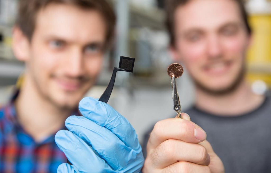
At this point, it’s possible I’m wrong but I think this is the first ‘memristor’ type device (also called a neuromorphic chip) based on light rather than electronics that I’ve featured here on this blog. In other words, it’s not, technically speaking, a memristor but it does have the same properties so it is a neuromorphic chip.

A May 8, 2019 news item on Nanowerk announces this new approach to neuromorphic hardware (Note: A link has been removed),
Researchers from the Universities of Münster (Germany), Oxford and Exeter (both UK) have succeeded in developing a piece of hardware which could pave the way for creating computers which resemble the human brain.
The scientists produced a chip containing a network of artificial neurons that works with light and can imitate the behaviour of neurons and their synapses. The network is able to “learn” information and use this as a basis for computing and recognizing patterns. As the system functions solely with light and not with electrons, it can process data many times faster than traditional systems. …
A May 8, 2019 University of Münster press release (also on EurekAlert), which originated the news item, reveals the full story,
A technology that functions like a brain? In these times of artificial intelligence, this no longer seems so far-fetched – for example, when a mobile phone can recognise faces or languages. With more complex applications, however, computers still quickly come up against their own limitations. One of the reasons for this is that a computer traditionally has separate memory and processor units – the consequence of which is that all data have to be sent back and forth between the two. In this respect, the human brain is way ahead of even the most modern computers because it processes and stores information in the same place – in the synapses, or connections between neurons, of which there are a million-billion in the brain. An international team of researchers from the Universities of Münster (Germany), Oxford and Exeter (both UK) have now succeeded in developing a piece of hardware which could pave the way for creating computers which resemble the human brain. The scientists managed to produce a chip containing a network of artificial neurons that works with light and can imitate the behaviour of neurons and their synapses.
The researchers were able to demonstrate, that such an optical neurosynaptic network is able to “learn” information and use this as a basis for computing and recognizing patterns – just as a brain can. As the system functions solely with light and not with traditional electrons, it can process data many times faster. “This integrated photonic system is an experimental milestone,” says Prof. Wolfram Pernice from Münster University and lead partner in the study. “The approach could be used later in many different fields for evaluating patterns in large quantities of data, for example in medical diagnoses.” The study is published in the latest issue of the “Nature” journal.
The story in detail – background and method used
Most of the existing approaches relating to so-called neuromorphic networks are based on electronics, whereas optical systems – in which photons, i.e. light particles, are used – are still in their infancy. The principle which the German and British scientists have now presented works as follows: optical waveguides that can transmit light and can be fabricated into optical microchips are integrated with so-called phase-change materials – which are already found today on storage media such as re-writable DVDs. These phase-change materials are characterised by the fact that they change their optical properties dramatically, depending on whether they are crystalline – when their atoms arrange themselves in a regular fashion – or amorphous – when their atoms organise themselves in an irregular fashion. This phase-change can be triggered by light if a laser heats the material up. “Because the material reacts so strongly, and changes its properties dramatically, it is highly suitable for imitating synapses and the transfer of impulses between two neurons,” says lead author Johannes Feldmann, who carried out many of the experiments as part of his PhD thesis at the Münster University.
In their study, the scientists succeeded for the first time in merging many nanostructured phase-change materials into one neurosynaptic network. The researchers developed a chip with four artificial neurons and a total of 60 synapses. The structure of the chip – consisting of different layers – was based on the so-called wavelength division multiplex technology, which is a process in which light is transmitted on different channels within the optical nanocircuit.
In order to test the extent to which the system is able to recognise patterns, the researchers “fed” it with information in the form of light pulses, using two different algorithms of machine learning. In this process, an artificial system “learns” from examples and can, ultimately, generalise them. In the case of the two algorithms used – both in so-called supervised and in unsupervised learning – the artificial network was ultimately able, on the basis of given light patterns, to recognise a pattern being sought – one of which was four consecutive letters.
“Our system has enabled us to take an important step towards creating computer hardware which behaves similarly to neurons and synapses in the brain and which is also able to work on real-world tasks,” says Wolfram Pernice. “By working with photons instead of electrons we can exploit to the full the known potential of optical technologies – not only in order to transfer data, as has been the case so far, but also in order to process and store them in one place,” adds co-author Prof. Harish Bhaskaran from the University of Oxford.
A very specific example is that with the aid of such hardware cancer cells could be identified automatically. Further work will need to be done, however, before such applications become reality. The researchers need to increase the number of artificial neurons and synapses and increase the depth of neural networks. This can be done, for example, with optical chips manufactured using silicon technology. “This step is to be taken in the EU joint project ‘Fun-COMP’ by using foundry processing for the production of nanochips,” says co-author and leader of the Fun-COMP project, Prof. C. David Wright from the University of Exeter.
Here’s a link to and a citation for the paper,
All-optical spiking neurosynaptic networks with self-learning capabilities by J. Feldmann, N. Youngblood, C. D. Wright, H. Bhaskaran & W. H. P. Pernice. Nature volume 569, pages208–214 (2019) DOI: https://doi.org/10.1038/s41586-019-1157-8 Issue Date: 09 May 2019
This paper is behind a paywall.
For the curious, I found a little more information about Fun-COMP (functionally-scaled computer technology). It’s a European Commission (EC) Horizon 2020 project coordinated through the University of Exeter. For information with details such as the total cost, contribution from the EC, the list of partnerships and more there is the Fun-COMP webpage on fabiodisconzi.com.
