Tag Archives: T. Taniguchi

The need for Wi-Fi speed

Yes, it’s a ‘Top Gun’ movie quote (1986) or more accurately, a paraphrasing of Tom Cruise’s line “I feel the need for speed.” I understand there’s a sequel, which is due to arrive in movie theatres or elsewhere at sometime in this decade.

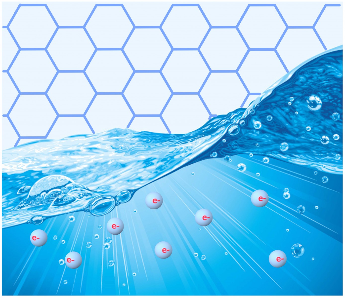
Where wireless and WiFi are concerned I think there is a dog/poodle situation. ‘Dog’ is a general description where ‘poodle’ is a specific description. All poodles (specific) are dogs (general) but not all dogs are poodles. So, wireless is a general description and Wi-Fi is a specific type of wireless communication. All WiFi is wireless but not all wireless is Wi-Fi. That said, onto the research.

Given what seems to be an insatiable desire for speed in the wireless world, the quote seems quite à propos in relation to the latest work on quantum tunneling and its impact on Wi-Fi speed from the Moscow Institute of Physics and Technology (from a February 3, 2021 news item on phys.org,

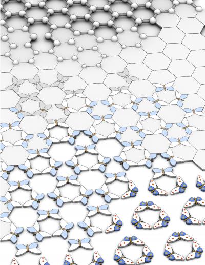
Scientists from MIPT (Moscow Institute of Physics and Technology), Moscow Pedagogical State University and the University of Manchester have created a highly sensitive terahertz detector based on the effect of quantum-mechanical tunneling in graphene. The sensitivity of the device is already superior to commercially available analogs based on semiconductors and superconductors, which opens up prospects for applications of the graphene detector in wireless communications, security systems, radio astronomy, and medical diagnostics. The research results are published in Nature Communications.

A February 3, 2021 MIPT press release (also on EurekAlert), which originated the news item, provides more technical detail about the work and its relation WiFi,

Information transfer in wireless networks is based on transformation of a high-frequency continuous electromagnetic wave into a discrete sequence of bits. This technique is known as signal modulation. To transfer the bits faster, one has to increase the modulation frequency. However, this requires synchronous increase in carrier frequency. A common FM-radio transmits at frequencies of hundred megahertz, a Wi-Fi receiver uses signals of roughly five gigahertz frequency, while the 5G mobile networks can transmit up to 20 gigahertz signals. This is far from the limit, and further increase in carrier frequency admits a proportional increase in data transfer rates. Unfortunately, picking up signals with hundred gigahertz frequencies and higher is an increasingly challenging problem.

A typical receiver used in wireless communications consists of a transistor-based amplifier of weak signals and a demodulator that rectifies the sequence of bits from the modulated signal. This scheme originated in the age of radio and television, and becomes inefficient at frequencies of hundreds of gigahertz desirable for mobile systems. The fact is that most of the existing transistors aren’t fast enough to recharge at such a high frequency.

An evolutionary way to solve this problem is just to increase the maximum operation frequency of a transistor. Most specialists in the area of nanoelectronics work hard in this direction. A revolutionary way to solve the problem was theoretically proposed in the beginning of 1990’s by physicists Michael Dyakonov and Michael Shur, and realized, among others, by the group of authors in 2018. It implies abandoning active amplification by transistor, and abandoning a separate demodulator. What’s left in the circuit is a single transistor, but its role is now different. It transforms a modulated signal into bit sequence or voice signal by itself, due to non-linear relation between its current and voltage drop.

In the present work, the authors have proved that the detection of a terahertz signal is very efficient in the so-called tunneling field-effect transistor. To understand its work, one can just recall the principle of an electromechanical relay, where the passage of current through control contacts leads to a mechanical connection between two conductors and, hence, to the emergence of current. In a tunneling transistor, applying voltage to the control contact (termed as ”gate”) leads to alignment of the energy levels of the source and channel. This also leads to the flow of current. A distinctive feature of a tunneling transistor is its very strong sensitivity to control voltage. Even a small “detuning” of energy levels is enough to interrupt the subtle process of quantum mechanical tunneling. Similarly, a small voltage at the control gate is able to “connect” the levels and initiate the tunneling current

“The idea of ??a strong reaction of a tunneling transistor to low voltages is known for about fifteen years,” says Dr. Dmitry Svintsov, one of the authors of the study, head of the laboratory for optoelectronics of two-dimensional materials at the MIPT center for photonics and 2D materials. “But it’s been known only in the community of low-power electronics. No one realized before us that the same property of a tunneling transistor can be applied in the technology of terahertz detectors. Georgy Alymov (co-author of the study) and I were lucky to work in both areas. We realized then: if the transistor is opened and closed at a low power of the control signal, then it should also be good in picking up weak signals from the ambient surrounding. “

The created device is based on bilayer graphene, a unique material in which the position of energy levels (more strictly, the band structure) can be controlled using an electric voltage. This allowed the authors to switch between classical transport and quantum tunneling transport within a single device, with just a change in the polarities of the voltage at the control contacts. This possibility is of extreme importance for an accurate comparison of the detecting ability of a classical and quantum tunneling transistor.

The experiment showed that the sensitivity of the device in the tunnelling mode is few orders of magnitude higher than that in the classical transport mode. The minimum signal distinguishable by the detector against the noisy background already competes with that of commercially available superconducting and semiconductor bolometers. However, this is not the limit – the sensitivity of the detector can be further increased in “cleaner” devices with a low concentration of residual impurities. The developed detection theory, tested by the experiment, shows that the sensitivity of the “optimal” detector can be a hundred times higher.

“The current characteristics give rise to great hopes for the creation of fast and sensitive detectors for wireless communications,” says the author of the work, Dr. Denis Bandurin. And this area is not limited to graphene and is not limited to tunnel transistors. We expect that, with the same success, a remarkable detector can be created, for example, based on an electrically controlled phase transition. Graphene turned out to be just a good launching pad here, just a door, behind which is a whole world of exciting new research.”

The results presented in this paper are an example of a successful collaboration between several research groups. The authors note that it is this format of work that allows them to obtain world-class scientific results. For example, earlier, the same team of scientists demonstrated how waves in the electron sea of ??graphene can contribute to the development of terahertz technology. “In an era of rapidly evolving technology, it is becoming increasingly difficult to achieve competitive results.” – comments Dr. Georgy Fedorov, deputy head of the nanocarbon materials laboratory, MIPT, – “Only by combining the efforts and expertise of several groups can we successfully realize the most difficult tasks and achieve the most ambitious goals, which we will continue to do.”

Here’s a link to and a citation for the latest paper,

Tunnel field-effect transistors for sensitive terahertz detection by I. Gayduchenko, S. G. Xu, G. Alymov, M. Moskotin, I. Tretyakov, T. Taniguchi, K. Watanabe, G. Goltsman, A. K. Geim, G. Fedorov, D. Svintsov & D. A. Bandurin. Nature Communications volume 12, Article number: 543 (2021) DOI: https://doi.org/10.1038/s41467-020-20721-z Published: 22 January 2021

This paper is open access.

One last comment, I’m assuming since the University of Manchester is mentioned that A. K. Geim is Sir Andre K. Geim (you can look him up here is you’re not familiar with his role in the graphene research community).

A new wave of physics: electrons flow like liquid in graphene

Unfortunately I couldn’t find a credit for the artist for the graphic (I really like it) which accompanies the news about a new physics and graphene,

Courtesy: University of Manchester

From an Aug. 22, 2017 news item on phys.org (Note: A link has been removed),

A new understanding of the physics of conductive materials has been uncovered by scientists observing the unusual movement of electrons in graphene.

Graphene is many times more conductive than copper thanks, in part, to its two-dimensional structure. In most metals, conductivity is limited by crystal imperfections which cause electrons to frequently scatter like billiard balls when they move through the material.

Now, observations in experiments at the National Graphene Institute have provided essential understanding as to the peculiar behaviour of electron flows in graphene, which need to be considered in the design of future Nano-electronic circuits.

An Aug. 22, 2017 University of Manchester press release, which originated the news item, delves further into the research (Note: Links have been removed),

Appearing today in Nature Physics, researchers at The University of Manchester, in collaboration with theoretical physicists led by Professor Marco Polini and Professor Leonid Levitov, show that Landauer’s fundamental limit can be breached in graphene. Even more fascinating is the mechanism responsible for this.

Last year, a new field in solid-state physics termed ‘electron hydrodynamics’ generated huge scientific interest. Three different experiments, including one performed by The University of Manchester, demonstrated that at certain temperatures, electrons collide with each other so frequently they start to flow collectively like a viscous fluid.

The new research demonstrates that this viscous fluid is even more conductive than ballistic electrons. The result is rather counter-intuitive, since typically scattering events act to lower the conductivity of a material, because they inhibit movement within the crystal. However, when electrons collide with each other, they start working together and ease current flow.

This happens because some electrons remain near the crystal edges, where momentum dissipation is highest, and move rather slowly. At the same time, they protect neighbouring electrons from colliding with those regions. Consequently, some electrons become super-ballistic as they are guided through the channel by their friends.

Sir Andre Geim said: “We know from school that additional disorder always creates extra electrical resistance. In our case, disorder induced by electron scattering actually reduces rather than increase resistance. This is unique and quite counterintuitive: Electrons when make up a liquid start propagating faster than if they were free, like in vacuum”.

The researchers measured the resistance of graphene constrictions, and found it decreases upon increasing temperature, in contrast to the usual metallic behaviour expected for doped graphene.

By studying how the resistance across the constrictions changes with temperature, the scientists revealed a new physical quantity which they called the viscous conductance. The measurements allowed them to determine electron viscosity to such a high precision that the extracted values showed remarkable quantitative agreement with theory.

Here’s a link to and a citation for the paper,

Superballistic flow of viscous electron fluid through graphene constrictions by R. Krishna Kumar, D. A. Bandurin, F. M. D. Pellegrino, Y. Cao, A. Principi, H. Guo, G. H. Auton, M. Ben Shalom, L. A. Ponomarenko, G. Falkovich, K. Watanabe, T. Taniguchi, I. V. Grigorieva, L. S. Levitov, M. Polini, & A. K. Geim. Nature Physics (2017) doi:10.1038/nphys4240 Published online 21 August 2017

This paper is behind a paywall.

Three teams observe graphene butterflies

It took me a few minutes to find the butterflies (visual pattern recognition is not one of my strengths) but here they are,

Caption: Graphene, combined with white graphene, forms stunning 'butterfly' images. Credit: The University of Manchester

Caption: Graphene, combined with white graphene, forms stunning ‘butterfly’ images.
Credit: The University of Manchester

The May 15, 2013 University of Manchester news release (on EurekAlert and on the University of Manchester news site) describes how the ‘butterflies’ are formed,

Writing in Nature, a large international team led Dr Roman Gorbachev from The University of Manchester shows that, when graphene placed on top of insulating boron nitride, or ‘white graphene’, the electronic properties of graphene change dramatically revealing a pattern resembling a butterfly.

The pattern is referred to as the elusive Hofstadter butterfly that has been known in theory for many decades but never before observed in experiments.

More of the science needs to be explained before moving on with the ‘butterflies’ (from the news release),

One of the most remarkable properties of graphene is its high conductivity – thousands of times higher than copper. This is due to a very special pattern created by electrons that carry electricity in graphene. The carriers are called Dirac fermions and mimic massless relativistic particles called neutrinos, studies of which usually require huge facilities such as at CERN. The possibility to address similar physics in a desk-top experiment is one of the most renowned features of graphene.

Now the Manchester scientists have found a way to create multiple clones of Dirac fermions. Graphene is placed on top of boron nitride so that graphene’s electrons can ‘feel’ individual boron and nitrogen atoms. Moving along this atomic ‘washboard’, electrons rearrange themselves once again producing multiple copies of the original Dirac fermions.

Here’s where the butterflies appear (from the news release),

The researchers can create even more clones by applying a magnetic field. The clones produce an intricate pattern; the Hofstadter butterfly. It was first predicted by mathematician Douglas Hofstadter in 1976 and, despite many dedicated experimental efforts, no more than a blurred glimpse was reported before.

In addition to the described fundamental interest, the Manchester study proves that it is possible to modify properties of atomically-thin materials by placing them on top of each other. This can be useful, for example, for graphene applications such as ultra-fast photodetectors and transistors, providing a way to tweak its incredible properties.

Coincidentally, another team has also observed the Hofstadter butterfly on a graphene substrate. From the May 16, 2013 news item on Azonano,

Two research teams at the National High Magnetic Field Laboratory (MagLab) broke through a nearly 40-year barrier recently when they observed a never-before-seen energy pattern.

“The observation of the ‘Hofstadter butterfly’ marks a real landmark in condensed matter physics and high magnetic field research,” said Greg Boebinger, director of the MagLab. “It opens a new experimental direction in materials research.”

This groundbreaking research demanded the ability to measure samples of materials at very low temperatures and very high magnetic fields, up to 35 tesla. Both of those conditions are available at the MagLab, making it an international destination for scientific exploration.

The unique periodic structure used to observe the butterfly pattern was composed of boron nitride (BN) and graphene.

The May 15, 2013 Florida State University news release by Kristin Roberts, which originated the news item, describes the two teams using the MagLab facilities for their ‘butterfly’ observations,

One research team was led by Columbia University’s Philip Kim and included researchers from City University of New York, the University of Central Florida, Tohoku University and the National Institute for Materials Science in Japan. The team’s work will be published today in the Advanced Online Publication of the journal Nature. Similar results were discovered at the MagLab by a group led by Pablo Jarillo-Herrero and Raymond Ashoori at MIT, as well as scientists from Tohoku University and the National Institute for Materials Science in Japan. Their work is expected to be published soon.

For those who just can’t get enough graphene butterflies here are citations for and links to both recently published papers (the Jarillo-Herrero/Ashoori team will be publishing their work soon).

Cloning of Dirac fermions in graphene superlattices by L. A. Ponomarenko, R. V. Gorbachev, G. L. Yu,D. C. Elias, R. Jalil, A. A. Patel, A. Mishchenko, A. S. Mayorov, C. R. Woods, J. R. Wallbank, M. Mucha-Kruczynski, B. A. Piot, M. Potemski, I. V. Grigorieva, K. S. Novoselov, F. Guinea, V. I. Fal’ko & A. K. Geim. Nature doi:10.1038/nature12187 Published online   

and,

Hofstadter’s butterfly and the fractal quantum Hall effect in moiré superlattices by C. R. Dean, L. Wang, P. Maher, C. Forsythe, F. Ghahari, Y. Gao, J. Katoch, M. Ishigami, P. Moon, M. Koshino, T. Taniguchi, K. Watanabe, K. L. Shepard, J. Hone & P. Kim. Nature (2013) doi:10.1038/nature12186 Published online 15 May 2013

Both papers are behind paywalls.