About 2.5 years ago there was an article titled, “A roadmap for graphene” (behind a paywall) which Nature magazine published online in Oct. 2012. I see at least two of the 2012 authors, Konstantin (Kostya) Novoselov and Vladimir Fal’ko,, are party to this second, more comprehensive roadmap featured in a Feb. 24, 2015 news item on Nanowerk,
In October 2013, academia and industry came together to form the Graphene Flagship. Now with 142 partners in 23 countries, and a growing number of associate members, the Graphene Flagship was established following a call from the European Commission to address big science and technology challenges of the day through long-term, multidisciplinary R&D efforts.
A Feb. 24, 2015 University of Cambridge news release, which originated the news item, describes the roadmap in more detail,
In an open-access paper published in the Royal Society of Chemistry journal Nanoscale, more than 60 academics and industrialists lay out a science and technology roadmap for graphene, related two-dimensional crystals, other 2D materials, and hybrid systems based on a combination of different 2D crystals and other nanomaterials. The roadmap covers the next ten years and beyond, and its objective is to guide the research community and industry toward the development of products based on graphene and related materials.
…
The roadmap highlights three broad areas of activity. The first task is to identify new layered materials, assess their potential, and develop reliable, reproducible and safe means of producing them on an industrial scale. Identification of new device concepts enabled by 2D materials is also called for, along with the development of component technologies. The ultimate goal is to integrate components and structures based on 2D materials into systems capable of providing new functionalities and application areas.
Eleven science and technology themes are identified in the roadmap. These are: fundamental science, health and environment, production, electronic devices, spintronics, photonics and optoelectronics, sensors, flexible electronics, energy conversion and storage, composite materials, and biomedical devices. The roadmap addresses each of these areas in turn, with timelines.
Research areas outlined in the roadmap correspond broadly with current flagship work packages, with the addition of a work package devoted to the growing area of biomedical applications, to be included in the next phase of the flagship. A recent independent assessment has confirmed that the Graphene Flagship is firmly on course, with hundreds of research papers, numerous patents and marketable products to its name.
Roadmap timelines predict that, before the end of the ten-year period of the flagship, products will be close to market in the areas of flexible electronics, composites, and energy, as well as advanced prototypes of silicon-integrated photonic devices, sensors, high-speed electronics, and biomedical devices.
“This publication concludes a four-year effort to collect and coordinate state-of-the-art science and technology of graphene and related materials,” says Andrea Ferrari, director of the Cambridge Graphene Centre, and chairman of the Executive Board of the Graphene Flagship. “We hope that this open-access roadmap will serve as the starting point for academia and industry in their efforts to take layered materials and composites from laboratory to market.” Ferrari led the roadmap effort with Italian Institute of Technology physicist Francesco Bonaccorso, who is a Royal Society Newton Fellow of the University of Cambridge, and a Fellow of Hughes Hall.
“We are very proud of the joint effort of the many authors who have produced this roadmap,” says Jari Kinaret, director of the Graphene Flagship. “The roadmap forms a solid foundation for the graphene community in Europe to plan its activities for the coming years. It is not a static document, but will evolve to reflect progress in the field, and new applications identified and pursued by industry.”
I have skimmed through the report briefly (wish I had more time) and have a couple of comments. First, there’s an excellent glossary of terms for anyone who might stumble over chemical abbreviations and/or more technical terminology. Second, they present a very interesting analysis of the intellectual property (patents) landscape (Note: Links have been removed. Incidental numbers are footnote references),
In the graphene area, there has been a particularly rapid increase in patent activity from around 2007.45 Much of this is driven by patent applications made by major corporations and universities in South Korea and USA.53 Additionally, a high level of graphene patent activity in China is also observed.54 These features have led some commentators to conclude that graphene innovations arising in Europe are being mainly exploited elsewhere.55 Nonetheless, an analysis of the Intellectual Property (IP) provides evidence that Europe already has a significant foothold in the graphene patent landscape and significant opportunities to secure future value. As the underlying graphene technology space develops, and the GRM [graphene and related materials] patent landscape matures, re-distribution of the patent landscape seems inevitable and Europe is well positioned to benefit from patent-based commercialisation of GRM research.
Overall, the graphene patent landscape is growing rapidly and already resembles that of sub-segments of the semiconductor and biotechnology industries,56 which experience high levels of patent activity. The patent strategies of the businesses active in such sub-sectors frequently include ‘portfolio maximization’56 and ‘portfolio optimization’56 strategies, and the sub-sectors experience the development of what commentators term ‘patent thickets’56, or multiple overlapping granted patent rights.56 A range of policies, regulatory and business strategies have been developed to limit such patent practices.57 In such circumstances, accurate patent landscaping may provide critical information to policy-makers, investors and individual industry participants, underpinning the development of sound policies, business strategies and research commercialisation plans.
It sounds like a patent thicket is developing (Note: Links have been removed. Incidental numbers are footnote references),,
Fig. 13 provides evidence of a relative increase in graphene patent filings in South Korea from 2007 to 2009 compared to 2004–2006. This could indicate increased commercial interest in graphene technology from around 2007. The period 2010 to 2012 shows a marked relative increase in graphene patent filings in China. It should be noted that a general increase in Chinese patent filings across many ST domains in this period is observed.76 Notwithstanding this general increase in Chinese patent activity, there does appear to be increased commercial interest in graphene in China. It is notable that the European Patent Office contribution as a percentage of all graphene patent filings globally falls from a 8% in the period 2007 to 2009 to 4% in the period 2010 to 2012.
The importance of the US, China and South Korea is emphasised by the top assignees, shown in Fig. 14. The corporation with most graphene patent applications is the Korean multinational Samsung, with over three times as many filings as its nearest rival. It has also patented an unrivalled range of graphene-technology applications, including synthesis procedures,77 transparent display devices,78 composite materials,79 transistors,80 batteries and solar cells.81 Samsung’s patent applications indicate a sustained and heavy investment in graphene R&D, as well as collaboration (co-assignment of patents) with a wide range of academic institutions.82,83
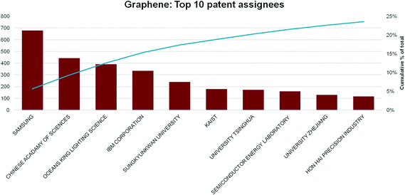 |
|
Fig. 14 Top 10 graphene patent assignees by number and cumulative over all time as of end-July 2014. Number of patents are indicated in the red histograms referred to the left Y axis, while the cumulative percentage is the blue line, referred to the right Y axis. |
|
It is also interesting to note that patent filings by universities and research institutions make up a significant proportion (![[similar]](http://www.rsc.org/images/entities/char_223c.gif) 50%) of total patent filings: the other half comprises contributions from small and medium-sized enterprises (SMEs) and multinationals.
50%) of total patent filings: the other half comprises contributions from small and medium-sized enterprises (SMEs) and multinationals.
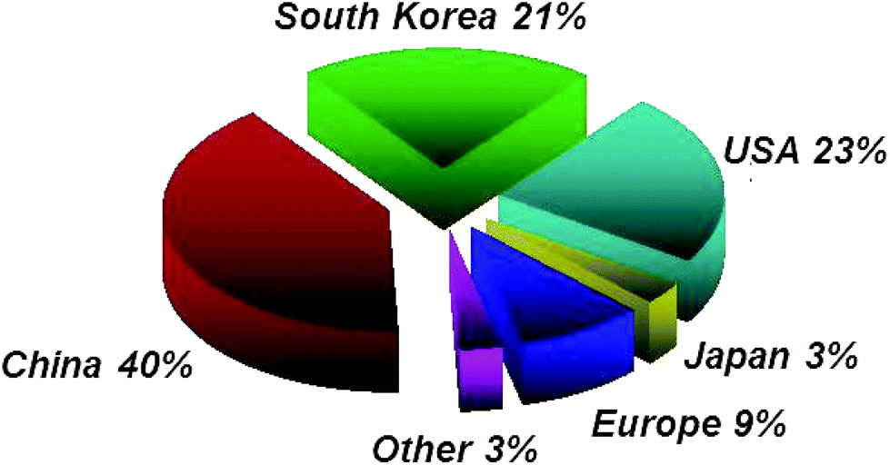
Europe’s position is shown in Fig. 10, 12 and 14. While Europe makes a good showing in the geographical distribution of publications, it lags behind in patent applications, with only 7% of patent filings as compared to 30% in the US, 25% in China, and 13% in South Korea (Fig. 13) and only 9% of filings by academic institutions assigned in Europe (Fig. 15).
 |
|
Fig. 15 Geographical breakdown of academic patent holders as of July 2014. |
|
While Europe is trailing other regions in terms of number of patent filings, it nevertheless has a significant foothold in the patent landscape. Currently, the top European patent holder is Finland’s Nokia, primarily around incorporation of graphene into electrical devices, including resonators and electrodes.72,84,85
This may sound like Europe is trailing behind but that’s not the case according to the roadmap (Note: Links have been removed. Incidental numbers are footnote references),
European Universities also show promise in the graphene patent landscape. We also find evidence of corporate-academic collaborations in Europe, including e.g. co-assignments filed with European research institutions and Germany’s AMO GmbH,86 and chemical giant BASF.87,88 Finally, Europe sees significant patent filings from a number of international corporate and university players including Samsung,77 Vorbeck Materials,89 Princeton University,90–92 and Rice University,93–95 perhaps reflecting the quality of the European ST base around graphene, and its importance as a market for graphene technologies.
There are a number of features in the graphene patent landscape which may lead to a risk of patent thickets96 or ‘multiple overlapping granted patents’ existing around aspects of graphene technology systems. [emphasis mine] There is a relatively high volume of patent activity around graphene, which is an early stage technology space, with applications in patent intensive industry sectors. Often patents claim carbon nano structures other than graphene in graphene patent landscapes, illustrating difficulties around defining ‘graphene’ and mapping the graphene patent landscape. Additionally, the graphene patent nomenclature is not entirely settled. Different patent examiners might grant patents over the same components which the different experts and industry players call by different names.
For anyone new to this blog, I am not a big fan of current patent regimes as they seem to be stifling rather encouraging innovation. Sadly, patents and copyright were originally developed to encourage creativity and innovation by allowing the creators to profit from their ideas. Over time a system designed to encourage innovation has devolved into one that does the opposite. (My Oct. 31, 2011 post titled Patents as weapons and obstacles, details my take on this matter.) I’m not arguing against patents and copyright but suggesting that the system be fixed or replaced with something that delivers on the original intention.
Getting back to the matter at hand, here’s a link to and a citation for the 200 pp. 2015 European Graphene roadmap,
Science and technology roadmap for graphene, related two-dimensional crystals, and hybrid systems by Andrea C. Ferrari, Francesco Bonaccorso, Vladimir Fal’ko, Konstantin S. Novoselov, Stephan Roche, Peter Bøggild, Stefano Borini, Frank H. L. Koppens, Vincenzo Palermo, Nicola Pugno, José A. Garrido, Roman Sordan, Alberto Bianco, Laura Ballerini, Maurizio Prato, Elefterios Lidorikis, Jani Kivioja, Claudio Marinelli, Tapani Ryhänen, Alberto Morpurgo, Jonathan N. Coleman, Valeria Nicolosi, Luigi Colombo, Albert Fert, Mar Garcia-Hernandez, Adrian Bachtold, Grégory F. Schneider, Francisco Guinea, Cees Dekker, Matteo Barbone, Zhipei Sun, Costas Galiotis, Alexander N. Grigorenko, Gerasimos Konstantatos, Andras Kis, Mikhail Katsnelson, Lieven Vandersypen, Annick Loiseau, Vittorio Morandi, Daniel Neumaier, Emanuele Treossi, Vittorio Pellegrini, Marco Polini, Alessandro Tredicucci, Gareth M. Williams, Byung Hee Hong, Jong-Hyun Ahn, Jong Min Kim, Herbert Zirath, Bart J. van Wees, Herre van der Zant, Luigi Occhipinti, Andrea Di Matteo, Ian A. Kinloch, Thomas Seyller, Etienne Quesnel, Xinliang Feng, Ken Teo, Nalin Rupesinghe, Pertti Hakonen, Simon R. T. Neil, Quentin Tannock, Tomas Löfwander and Jari Kinaret. Nanoscale, 2015, Advance Article DOI: 10.1039/C4NR01600A First published online 22 Sep 2014
Here’s a diagram illustrating the roadmap process,
![Fig. 122 The STRs [science and technology roadmaps] follow a hierarchical structure where the strategic level in a) is connected to the more detailed roadmap shown in b). These general roadmaps are the condensed form of the topical roadmaps presented in the previous sections, and give technological targets for key applications to become commercially competitive and the forecasts for when the targets are predicted to be met. Courtesy: Researchers and the Royal Society's journal, Nanoscale](http://www.frogheart.ca/wp-content/uploads/2015/02/Euroepan-Graphene-Roadmap-203x300.gif)
Fig. 122 The STRs [science and technology roadmaps] follow a hierarchical structure where the strategic level in a) is connected to the more detailed roadmap shown in b). These general roadmaps are the condensed form of the topical roadmaps presented in the previous sections, and give technological targets for key applications to become commercially competitive and the forecasts for when the targets are predicted to be met.
Courtesy: Researchers and the Royal Society’s journal, Nanoscale
The image here is not the best quality; the one embedded in the relevant Nanowerk
news item is better.
As for the earlier roadmap, here’s my Oct. 11, 2012 post on the topic.


![Fig. 122 The STRs [science and technology roadmaps] follow a hierarchical structure where the strategic level in a) is connected to the more detailed roadmap shown in b). These general roadmaps are the condensed form of the topical roadmaps presented in the previous sections, and give technological targets for key applications to become commercially competitive and the forecasts for when the targets are predicted to be met. Courtesy: Researchers and the Royal Society's journal, Nanoscale](http://www.frogheart.ca/wp-content/uploads/2015/02/Euroepan-Graphene-Roadmap.gif)