Tag Archives: CVD

Scaling graphene production up to industrial strength

If graphene is going to be a ubiquitous material in the future, production methods need to change. An Aug. 7, 2015 news item on Nanowerk announces a new technique to achieve that goal,

Producing graphene in bulk is critical when it comes to the industrial exploitation of this exceptional two-dimensional material. To that end, [European Commission] Graphene Flagship researchers have developed a novel variant on the chemical vapour deposition process which yields high quality material in a scalable manner. This advance should significantly narrow the performance gap between synthetic and natural graphene.

An Aug. 7, 2015 European Commission Graphene Flagship press release by Francis Sedgemore, which originated the news item, describes the problem,

Media-friendly Nobel laureates peeling layers of graphene from bulk graphite with sticky tape may capture the public imagination, but as a manufacturing process the technique is somewhat lacking. Mechanical exfoliation may give us pristine graphene, but industry requires scalable and cost-effective production processes with much higher yields.

On to the new method (from the press release),

Flagship-affiliated physicists from RWTH Aachen University and Forschungszentrum Jülich have together with colleagues in Japan devised a method for peeling graphene flakes from a CVD substrate with the help of intermolecular forces. …

Key to the process is the strong van der Waals interaction that exists between graphene and hexagonal boron nitride, another 2d material within which it is encapsulated. The van der Waals force is the attractive sum of short-range electric dipole interactions between uncharged molecules.

Thanks to strong van der Waals interactions between graphene and boron nitride, CVD graphene can be separated from the copper and transferred to an arbitrary substrate. The process allows for re-use of the catalyst copper foil in further growth cycles, and minimises contamination of the graphene due to processing.

Raman spectroscopy and transport measurements on the graphene/boron nitride heterostructures reveals high electron mobilities comparable with those observed in similar assemblies based on exfoliated graphene. Furthermore – and this comes as something of a surprise to the researchers – no noticeable performance changes are detected between devices developed in the first and subsequent growth cycles. This confirms the copper as a recyclable resource in the graphene fabrication process.

“Chemical vapour deposition is a highly scalable and cost-efficient technology,” says Christoph Stampfer, head of the 2nd Institute of Physics A in Aachen, and co-author of the technical article. “Until now, graphene synthesised this way has been significantly lower in quality than that obtained with the scotch-tape method, especially when it comes to the material’s electronic properties. But no longer. We demonstrate a novel fabrication process based on CVD that yields ultra-high quality synthetic graphene samples. The process is in principle suitable for industrial-scale production, and narrows the gap between graphene research and its technological applications.”

With their dry-transfer process, Banszerus and his colleagues have shown that the electronic properties of CVD-grown graphene can in principle match those of ultrahigh-mobility exfoliated graphene. The key is to transfer CVD graphene from its growth substrate in such a way that chemical contamination is avoided. The high mobility of pristine graphene is thus preserved, and the approach allows for the substrate material to be recycled without degradation.

Here’s a link to and citation for the paper,

Ultrahigh-mobility graphene devices from chemical vapor deposition on reusable copper by Luca Banszerus, Michael Schmitz, Stephan Engels, Jan Dauber, Martin Oellers, Federica Haupt, Kenji Watanabe, Takashi Taniguchi, Bernd Beschoten, and Christoph Stampfer. Science Advances  31 Jul 2015: Vol. 1, no. 6, e1500222 DOI: 10.1126/sciadv.1500222

This article appears to be open access.

For those interested in finding out more about chemical vapour deposition (CVD), David Chandler has written a June 19, 2015 article for the Massachusetts Institute of Technology (MIT) titled:  Explained: chemical vapor deposition (Technique enables production of pure, uniform coatings of metals or polymers, even on contoured surfaces.)
Serendipity and coaxial nanocables

I like the sound of the word coaxial especially when it’s used in conjunction with cable, as in coaxial cable. Adding the world serendipity to the mix, as they did at Rice University, made the June 7, 2012 news item by Jade Boyd on the Nanowerk website irresistible [Note: I have removed a link.],

Thanks to a little serendipity, researchers at Rice University have created a tiny coaxial cable that is about a thousand times smaller than a human hair and has higher capacitance than previously reported microcapacitors.

The nanocable, which is described this week in Nature Communications (“Anomalous high capacitance in a coaxial single nanowire capacitor” [behind paywall]), was produced with techniques pioneered in the nascent graphene research field and could be used to build next-generation energy-storage systems. It could also find use in wiring up components of lab-on-a-chip processors, but its discovery is owed partly to chance.

“We didn’t expect to create this when we started,” said study co-author Jun Lou, associate professor of mechanical engineering and materials science at Rice. “At the outset, we were just curious to see what would happen electrically and mechanically if we took small copper wires known as interconnects and covered them with a thin layer of carbon.”

Boyd’s June 7, 2012 news item can also be read in its entirety at the Rice University website [Note: I have removed some links.],

The tiny coaxial cable is remarkably similar in makeup to the ones that carry cable television signals into millions of homes and offices. The heart of the cable is a solid copper wire that is surrounded by a thin sheath of insulating copper oxide. A third layer, another conductor, surrounds that. In the case of TV cables, the third layer is copper again, but in the nanocable it is a thin layer of carbon measuring just a few atoms thick. The coax nanocable is about 100 nanometers, or 100 billionths of a meter, wide.

While the coaxial cable is a mainstay of broadband telecommunications, the three-layer, metal-insulator-metal structure can also be used to build energy-storage devices called capacitors. Unlike batteries, which rely on chemical reactions to both store and supply electricity, capacitors use electrical fields. A capacitor contains two electrical conductors, one negative and the other positive, that are separated by thin layer of insulation. Separating the oppositely charged conductors creates an electrical potential, and that potential increases as the separated charges increase and as the distance between them – occupied by the insulating layer — decreases. The proportion between the charge density and the separating distance is known as capacitance, and it’s the standard measure of efficiency of a capacitor.

The study reports that the capacitance of the nanocable is at least 10 times greater than what would be predicted with classical electrostatics.

“The increase is most likely due to quantum effects that arise because of the small size of the cable,” said study co-author Pulickel Ajayan, Rice’s Benjamin M. and Mary Greenwood Anderson Professor of Mechanical Engineering and Materials Science.

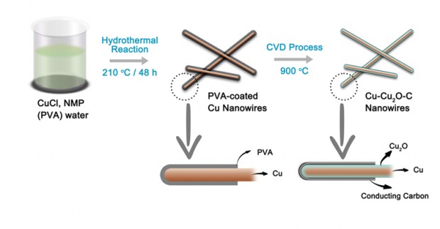
When the project began 18 months ago, Rice postdoctoral researcher Zheng Liu, the lead co-author of the study, intended to make pure copper wires covered with carbon. The techniques for making the wires, which are just a few nanometers wide, are well-established because the wires are often used as “interconnects” in state-of-the-art electronics. Liu used a technique known as chemical vapor deposition (CVD) to cover the wires with a thin coating of carbon. The CVD technique is also used to grow sheets of single-atom-thick carbon called graphene on films of copper.

“When people make graphene, they usually want to study the graphene and they aren’t very interested in the copper,” Lou said. “It’s just used a platform for making the graphene.”

When Liu ran some electronic tests on his first few samples, the results were far from what he expected.

“We eventually found that a thin layer of copper oxide — which is served as a dielectric layer — was forming between the copper and the carbon,” said Liu.

Here’s an image illustrating this process,

The three-layer coaxial nanocable contains a solid copper wire surrounded by a layer of copper oxide that is encased a layer of carbon just a few atoms thick. (Courtesy: Rice University)

The researchers don’t seem to have any particular applications in mind for their nancoaxial cable although they seem hopeful about a few possibilities (from the June 7, 2012 news item on the Rice University website,

The capacitance of the new nanocable is up to 143 microfarads per centimeter squared, better than the best previous results from microcapacitors.

Lou said it may be possible to build a large-scale energy-storage device by arranging millions of the tiny nanocables side by side in large arrays.

“The nanoscale cable might also be used as a transmission line for radio frequency signals at the nanoscale,” Liu said. “This could be useful as a fundamental building block in micro- and nano-sized electromechanical systems like lab-on-a-chip devices.”

Who knows where serendipity will take this discovery?

As for why that word made the item irresistible to me, many years ago I was at a dinner party and one of the guests (a vivid storyteller and born in Sri Lanka) explained the origin of the word, serendipity. Sadly I don’t remember the details of her story, so here’s a less rich version of the story from the Encyclopedia Britannia website,

Serendib, also spelled Serendip, Arabic Sarandīb, name for the island of Sri Lanka (Ceylon). The name, Arabic in origin, was recorded in use at least as early as ad 361 and for a time gained considerable currency in the West. It is best known to speakers of English through the word serendipity, invented in the 18th century by the English man of letters Horace Walpole on the inspiration of a Persian fairy tale, “The Three Princes of Serendip,” whose heroes often made discoveries by chance.