Tag Archives: Saarland University

Membrane stretching as a new transport mechanism for nanomaterials

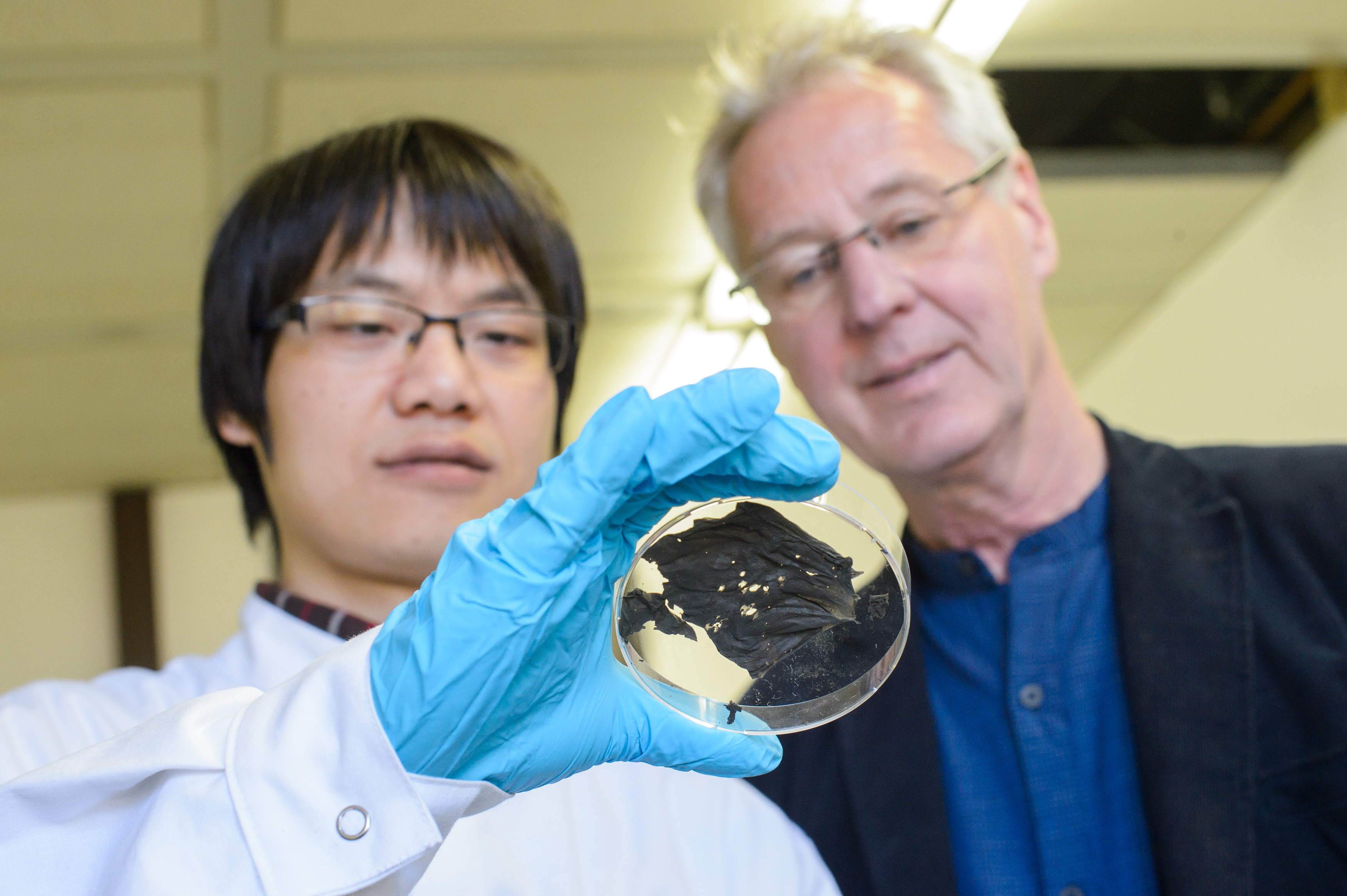
This work comes from Catalonia, Spain by way of a collaboration between Chinese, German, and, of course, Spanish scientists. From a December 12, 2018 Universitat Rovira i Virgili press release (also on EurekAlert),

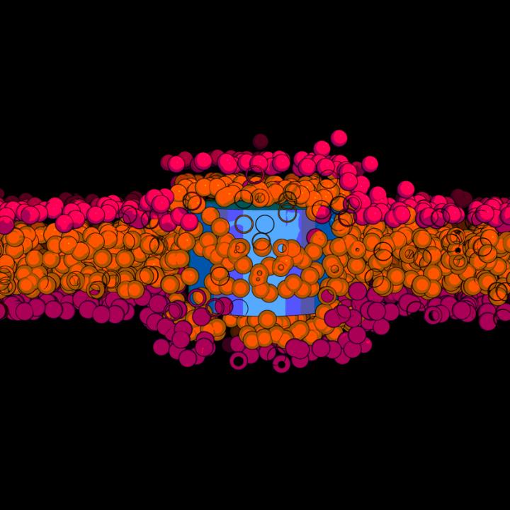
Increasing awareness of bioeffects and toxicity of nanomaterials interacting with cells puts in focus the mechanisms by which nanomaterials can cross lipid membranes. Apart from well-discussed energy-dependent endocytosis for large objects and passive diffusion through membranes by solute molecules, there can exist other transport mechanisms based on physical principles. Based on this hypothesis, the team of theoretical physics at Universitat Rovira i Virgili in Tarragona, led by Dr. Vladimir Baulin, designed a research project to investigate the interaction between nanotube and lipid membranes. In computer simulations, the researchers studied what they call a “model bilayer”, composed only by one type of lipids. Based on their calculations, the team of Dr. Baulin observed that ultra -short nanotube (10nm length) can insert perpendicularly to the lipid bilayer core.

They observed that these nanotubes stay trapped in the cell membrane, as commonly accepted by the scientific community. But a surprise appears when they stretched their model cell membrane, then inserted nanotubes which were trapped in the bilayer, suddenly started to escape from the bilayer on both sides. This means that it is possible to control the transport of nanomaterial across a cell membrane by tuning the membrane tension.

This is where Dr. Baulin contacted Dr. Jean-Baptiste Fleury at the Saarland University (Germany) to confirm this mechanism and to study experimentally this tension-mediated transport phenomena. Dr. Fleury and his team, designed a microfluidic experiment with a well-controlled phospholipid bilayer, an experimental model for cell membranes and added ultra-small carbon nanotubes (10nm in length) in solution. The nanotubes had an adsorbed lipid monolayer that guarantees their stable dispersion and prevent their clustering. Using a combination of optical fluorescent microscopy and electrophysiological measurements, the team of Dr. Fleury could follow individual nanotube crossing a bilayer and unravel their pathway on a molecular level. And as predicted by the simulations, they observed that nanotubes inserted into the bilayer by dissolving their lipid coating into the artificial membrane. When a tension of 4mN/m was applied to the bilayer, nanotubes spontaneously escaped the bilayer just in few milliseconds, while at lower tensions nanotubes remain trapped inside the membrane.

This discovery of translocation of tiny nanotubes through barriers protecting cells, i.e. lipid bilayer, may raise concerns about safety of nanomaterials for public health and suggest new mechanical mechanisms to control the drug delivery.

Caption: Nanotubes trapped inside the membrane. Credit: © URV

Here’s a link to and a citation for the paper,

Tension-Induced Translocation of an Ultrashort Carbon Nanotube through a Phospholipid Bilayer by Yachong Guo, Marco Werner, Ralf Seemann, Vladimir A. Baulin, and Jean-Baptiste Fleury. ACS Nano, Article ASAP DOI: 10.1021/acsnano.8b04657 Publication Date (Web): November 19, 2018

Copyright © 2018 American Chemical Society

This paper is behind a paywall.

Ultra-thin superconducting film for outer space

Truth in a press release? But first, there’s this April 6, 2017 news item on Nanowerk announcing research that may have applications in aerospace and other sectors,

Experimental physicists in the research group led by Professor Uwe Hartmann at Saarland University have developed a thin nanomaterial with superconducting properties. Below about -200 °C these materials conduct electricity without loss, levitate magnets and can screen magnetic fields.

The particularly interesting aspect of this work is that the research team has succeeded in creating superconducting nanowires that can be woven into an ultra-thin film that is as flexible as cling film. As a result, novel coatings for applications ranging from aerospace to medical technology are becoming possible.

The research team will be exhibiting their superconducting film at Hannover Messe from April 24th to April 28th [2017] (Hall 2, Stand B46) and are looking for commercial and industrial partners with whom they can develop their system for practical applications.

An April 6, 2017 University of Saarland press release (also on EurekAlert), which originated the news item, provides more details along with a line that rings with the truth,

A team of experimental physicists at Saarland University have developed something that – it has to be said – seems pretty unremarkable at first sight. [emphasis mine] It looks like nothing more than a charred black piece of paper. But appearances can be deceiving. This unassuming object is a superconductor. The term ‘superconductor’ is given to a material that (usually at a very low temperatures) has zero electrical resistance and can therefore conduct an electric current without loss. Put simply, the electrons in the material can flow unrestricted through the cold immobilized atomic lattice. In the absence of electrical resistance, if a magnet is brought up close to a cold superconductor, the magnet effectively ‘sees’ a mirror image of itself in the superconducting material. So if a superconductor and a magnet are placed in close proximity to one another and cooled with liquid nitrogen they will repel each another and the magnet levitates above the superconductor. The term ‘levitation’ comes from the Latin word levitas meaning lightness. It’s a bit like a low-temperature version of the hoverboard from the ‘Back to the Future’ films. If the temperature is too high, however, frictionless sliding is just not going to happen.
Many of the common superconducting materials available today are rigid, brittle and dense, which makes them heavy. The Saarbrücken physicists have now succeeded in packing superconducting properties into a thin flexible film. The material is a essentially a woven fabric of plastic fibres and high-temperature superconducting nanowires. ‘That makes the material very pliable and adaptable – like cling film (or ‘plastic wrap’ as it’s also known). Theoretically, the material can be made to any size. And we need fewer resources than are typically required to make superconducting ceramics, so our superconducting mesh is also cheaper to fabricate,’ explains Uwe Hartmann, Professor of Nanostructure Research and Nanotechnology at Saarland University.

The low weight of the film is particularly advantageous. ‘With a density of only 0.05 grams per cubic centimetre, the material is very light, weighing about a hundred times less than a conventional superconductor. This makes the material very promising for all those applications where weight is an issue, such as in space technology. There are also potential applications in medical technology,’ explains Hartmann. The material could be used as a novel coating to provide low-temperature screening from electromagnetic fields, or it could be used in flexible cables or to facilitate friction-free motion.

In order to be able to weave this new material, the experimental physicists made use of a technique known as electrospinning, which is usually used in the manufacture of polymeric fibres. ‘We force a liquid material through a very fine nozzle known as a spinneret to which a high electrical voltage has been applied. This produces nanowire filaments that are a thousand times thinner than the diameter of a human hair, typically about 300 nanometres or less. We then heat the mesh of fibres so that superconductors of the right composition are created. The superconducting material itself is typically an yttrium-barium-copper-oxide or similar compound,’ explains Dr. Michael Koblischka, one of the research scientists in Hartmann‘s group.

The research project received €100,000 in funding from the Volkswagen Foundation as part of its ‘Experiment!’ initiative. The initiative aims to encourage curiosity-driven, blue-skies research. The positive results from the Saarbrücken research team demonstrate the value of this type of funding. Since September 2016, the project has been supported by the German Research Foundation (DFG). Total funds of around €425,000 will be provided over a three-year period during which the research team will be carrying out more detailed investigations into the properties of the nanowires.

I’d say the “unremarkable but appearances can be deceiving” comments are true more often than not. I think that’s one of the hard things about science. Big advances can look nondescript.

What looks like a pretty unremarkable piece of burnt paper is in fact an ultrathin superconductor that has been developed by the team lead by Uwe Hartmann (r.) shown here with doctoral student XianLin Zeng. Courtesy: Saarland University

In any event, here’s a link to and a citation for the paper,

Preparation of granular Bi-2212 nanowires by electrospinning by Xian Lin Zeng, Michael R Koblischka, Thomas Karwoth, Thomas Hauet, and Uwe Hartmann. Superconductor Science and Technology, Volume 30, Number 3 Published 1 February 2017

© 2017 IOP Publishing Ltd

This paper is behind a paywall.

Trimming your electronics to size

It’s disconcerting to think that one might be able to trim down one’s electronic equipment at will but researchers at the Max Planck Institute for Informatics (Germany) and the Massachusetts Institute of Technology (MIT) have demonstrated that possibility,

An Oct. 8, 2013 news item on ScienceDaily describes this work which was presented today (Oct. 10, 2013) at  the ACM UIST conference in Scotland,

Today the researchers are presenting their work at the conference “User Interface and Technology” (UIST) in St. Andrews, Scotland.

“Imagine a kid takes our sensor film and cuts out a flower with stem and leaves. If you touch the blossom with a finger, you hear the buzzing of a bumblebee,” Jürgen Steimle says. He reports that programs and apps are easily imaginable to help parents connect touching a sensor film with the suitable sound effect. Steimle, 33, has a doctoral degree in computer science and is doing research at the Max-Planck Institute for Informatics. He also heads the Embodied Interaction research group at the Cluster of Excellence on Multimodal Computing and Interaction.

Simon Olberding is the doctoral candidate and the lead developer of the new sensor. He sees a further application of the new technology in so-called interactive walls used for discussions and brainstorming. “So far, such a wall frays and scuffs quickly as we hammer nails into it, stick notes or posters on it, and damage it while removing them. By customizing and pasting on our new sensor you can make every surface interactive no matter if it is the wristband of a watch, a cloth on a trade fair table, or wallpaper,” Olberding says.

As basic technology the scientists use so-called “printed electronics”. This term summarizes electrical components and devices which are printed. The approach is similar to that of inkjet printers. Instead of printing with normal ink, electrically-functional electronic ink is printed on flexible, thin films (so-called substrates). “The factory costs are so low that printing our DIN A4 film on our special printer in the lab costs us about one US dollar”, Steimle says.

The Oct. 8, 2013 Universität des Saarlandes (Saarland University) news release on EurekAlert, which originated the news item, describes how the researchers solved the problem of creating a system robust enough to withstand being cut,

But you need more than printed electronics to make a sensor robust against cuts, damage, and removed areas. So far the circuit layout of a multi-touch sensor has been similar to graph paper. The wires run horizontally, vertically, and parallel to each other. At the intersection of one parallel and one horizontal layer you find the touch-sensitive electrodes. Via the wires they are connected to a controller. This type of layout requires only a minimal number of wires, but is not robust. Since each wire addresses several electrodes, a small cut has a huge effect: many electrodes become unusable and possibly large sensor areas do not work anymore. “It was not easy to find an alternative layout, robust enough for our approach”, Olberding says. They took their inspiration from nature, looking at the human nerve system and fungal root networks, and thus came up with two basic layouts. The so-called star topology has the controller in the center. It is connected to every electrode separately. The so-called tree topology also has the controller in its center connected to each electrode separately. But the wires are bundled similarly to a tree structure. They all run through a vertical line in the middle and then branch off to reach their electrodes.

The scientists found out that the star topology supports often-used basic forms like triangles, rectangles, or ovals best. Furthermore, it is suitable for shapes commonly used for crafts, like stars, clouds, or hearts. In contrast, with the tree topology it is possible to cut out whole areas. The researchers were also able to combine both layouts in a space-saving way, so that the sensor supports all basic forms.

“We assume that printed sensors will be so inexpensive that multi-touch sensing capability will become an inherent part of the material. Users can take it to create interactive applications or just to write on it”, Steimle explains. This vision is not so far away, as a prediction from the “Organic and Printed Electronic Association” shows. The international industry association forecast that flexible consumer electronics will be available for end-users between the years 2017 and 2020.

Here’s a link to the unpublished paper,

A Cuttable Multi-touch Sensor by Simon Olberding, Nan-Wei Gong,John Tiab, Joseph A. Paradiso,  and Jürgen Steimle.

Enjoy!

Carbon nanotube art

With the help of laser beams material scientists from Saarbrücken have made nanotubes grown on a silicium plate and have generated structures that look under the scanning electron microscope as a jellyfish in the sea. For this picture, the researchers received the highest award in the nationwide photography competition "Nano sichtbar machen", which means “Make Nano visible”. Picture: "Nicolas Souza/cc-NanoBioNet e.V."

This was the winning image for a national photo competition sponsored by NanoBioNet, ASeNT-D and CeNTech (three German nanotechnology networks). From the Oct. 4, 2011 news item on Nanowerk,

Considered by some to be the “magic bullet” of materials science, carbon nanotubes (CNT) are at the forefront of materials research around the world. Carbon nanotubes are not only extremely stable, they are also excellent conductors of electrical energy and are made from a cheap raw material. Researchers at Saarland University want to use these highly versatile materials to help replace expensive precious metals in electrical contacts by cheaper alternatives such as nickel. By coating these replacement metals with nanotubes they hope to be able to prevent oxidation of the metal surface and thus avoid any associated reduction in electrical conductivity. By using lasers to help grow nanotubes on a silicon plate, the researchers in Saarbrücken have created structures that, when viewed under a scanning electron microscope, resemble a jellyfish in the ocean. This image was recently awarded first prize in the national photo competition “Making Nano Visible”.

More information can be found in the Oct. 4, 2011 news release issued by the Universität des Saarlandes,

The image taken by the Saarland University doctoral student Nicolas Souza may be used free of charge in connection with articles or other press coverage of Saarland University: http://www.uni-saarland.de/pressefotos

Pencils contain graphite, and graphite consists of carbon atoms aligned in layers. When we use a pencil for writing, these carbon atoms get deposited layer by layer. Nanotubes are essentially two-dimensional arrays of carbon atoms that have been rolled up as you would roll up a sheet of paper. “The result is tubes with a diameter of only ten nanometres, that is some 5000 times thinner than a human hair. These nanotubes are extremely stable and are also excellent conductors of electrical energy,” explains Nicolas Souza, doctoral student at the Department of Functional Materials headed by Professor Frank Mücklich. The challenge at present is to grow these nanotubes in a controlled way, such as depositing them as a lawn-like structure with the nanotubes attached to a contact surface. “We take a carbon mixture and by firing a laser at it we can raise the temperature of the target to about 6000° causing it to vaporize at that point. The vaporized carbon atoms deposit on a nickel-coated silicon plate located below and grow to form nanotubes that rise up from the plate. The nickel merely acts as a catalyst and is not consumed in the process. Viewed under a scanning electron microscope, the final product has the appearance of a jellyfish containing a red nickel core,” says Souza. His aim now is to try and establish even greater control over the growth process.

Congratulations to Nicolas Souza on his award-winning photography (the prize was 1000 Euros).