Neuromorphic computing is an information processing model that simulates the efficiency of the human brain with multifunctionality and flexibility. Currently, artificial synaptic devices represented by memristors have been extensively used in neural morphological computing, and different types of neural networks have been developed. However, it is time-consuming and laborious to perform fixing and redeploying of weights stored by traditional artificial synaptic devices. Moreover, synaptic strength is primarily reconstructed via software programming and changing the pulse time, which can result in low efficiency and high energy consumption in neural morphology computing applications.
In a novel research article published in the Beijing-based National Science Review, Prof. Lili Wang from the Chinese Academy of Sciences and her colleagues present a novel hardware neural network based on a tunable flexible MXene energy storage (FMES) system. The system comprises flexible postsynaptic electrodes and MXene nanosheets, which are connected with the presynaptic electrodes using electrolytes. The potential changes in the ion migration process and adsorption in the supercapacitor can simulate information transmission in the synaptic gap. Additionally, the voltage of the FMES system represents the synaptic weight of the connection between two neurons.
Researchers explored the changes of paired-pulse facilitation under different resistance levels to investigate the effect of resistance on the advanced learning and memory behavior of the artificial synaptic system of FMES. The results revealed that the larger the standard deviation, the stronger the memory capacity of the system. In other words, with the continuous improvement of electrical resistance and stimulation time, the memory capacity of the artificial synaptic system of FMES is gradually improved. Therefore, the system can effectively control the accumulation and dissipation of ions by regulating the resistance value in the system without changing the external stimulus, which is expected to realize the coupling of sensing signals and storage weight.
The FMES system can be used to develop neural networks and realize various neural morphological computing tasks, making the recognition accuracy of handwritten digit sets reach 95%. Additionally, the FMES system can simulate the adaptivity of the human brain to achieve adaptive recognition of similar target data sets. Following the training process, the adaptive recognition accuracy can reach approximately 80%, and avoid the time and energy loss caused by recalculation.
“In the future, based on this research, different types of sensors can be integrated on the chip to further realize multimodal sensing computing integrated architecture.” Prof. Lili Wang stated, “The device can perform low-energy calculations, and is expected to solve the problems of high write noise, nonlinear difference, and diffusion under zero bias voltage in certain neural morphological systems.”
*From the IOP’s Definitions of article versions: Accepted Manuscript is ‘the version of the article accepted for publication including all changes made as a result of the peer review process, and which may also include the addition to the article by IOP of a header, an article ID, a cover sheet and/or an ‘Accepted Manuscript’ watermark, but excluding any other editing, typesetting or other changes made by IOP and/or its licensors’.*
This is neither the published version nor the version of record.
An August 17, 2022 news item on Nanowerk announces big (so to speak) claims from a team researching neuromorphic (brainlike) computer chips,
An international team of researchers has designed and built a chip that runs computations directly in memory and can run a wide variety of artificial intelligence (AI) applications–all at a fraction of the energy consumed by computing platforms for general-purpose AI computing.
The NeuRRAM neuromorphic chip brings AI a step closer to running on a broad range of edge devices, disconnected from the cloud, where they can perform sophisticated cognitive tasks anywhere and anytime without relying on a network connection to a centralized server. Applications abound in every corner of the world and every facet of our lives, and range from smart watches, to VR headsets, smart earbuds, smart sensors in factories and rovers for space exploration.
The NeuRRAM chip is not only twice as energy efficient as the state-of-the-art “compute-in-memory” chips, an innovative class of hybrid chips that runs computations in memory, it also delivers results that are just as accurate as conventional digital chips. Conventional AI platforms are a lot bulkier and typically are constrained to using large data servers operating in the cloud.
In addition, the NeuRRAM chip is highly versatile and supports many different neural network models and architectures. As a result, the chip can be used for many different applications, including image recognition and reconstruction as well as voice recognition.
“The conventional wisdom is that the higher efficiency of compute-in-memory is at the cost of versatility, but our NeuRRAM chip obtains efficiency while not sacrificing versatility,” said Weier Wan, the paper’s first corresponding author and a recent Ph.D. graduate of Stanford University who worked on the chip while at UC San Diego, where he was co-advised by Gert Cauwenberghs in the Department of Bioengineering.
The research team, co-led by bioengineers at the University of California San Diego, presents their results in the Aug. 17 [2022] issue of Nature.
Currently, AI computing is both power hungry and computationally expensive. Most AI applications on edge devices involve moving data from the devices to the cloud, where the AI processes and analyzes it. Then the results are moved back to the device. That’s because most edge devices are battery-powered and as a result only have a limited amount of power that can be dedicated to computing.
By reducing power consumption needed for AI inference at the edge, this NeuRRAM chip could lead to more robust, smarter and accessible edge devices and smarter manufacturing. It could also lead to better data privacy as the transfer of data from devices to the cloud comes with increased security risks.
On AI chips, moving data from memory to computing units is one major bottleneck.
“It’s the equivalent of doing an eight-hour commute for a two-hour work day,” Wan said.
To solve this data transfer issue, researchers used what is known as resistive random-access memory, a type of non-volatile memory that allows for computation directly within memory rather than in separate computing units. RRAM and other emerging memory technologies used as synapse arrays for neuromorphic computing were pioneered in the lab of Philip Wong, Wan’s advisor at Stanford and a main contributor to this work. Computation with RRAM chips is not necessarily new, but generally it leads to a decrease in the accuracy of the computations performed on the chip and a lack of flexibility in the chip’s architecture.
“Compute-in-memory has been common practice in neuromorphic engineering since it was introduced more than 30 years ago,” Cauwenberghs said. “What is new with NeuRRAM is that the extreme efficiency now goes together with great flexibility for diverse AI applications with almost no loss in accuracy over standard digital general-purpose compute platforms.”
A carefully crafted methodology was key to the work with multiple levels of “co-optimization” across the abstraction layers of hardware and software, from the design of the chip to its configuration to run various AI tasks. In addition, the team made sure to account for various constraints that span from memory device physics to circuits and network architecture.
“This chip now provides us with a platform to address these problems across the stack from devices and circuits to algorithms,” said Siddharth Joshi, an assistant professor of computer science and engineering at the University of Notre Dame , who started working on the project as a Ph.D. student and postdoctoral researcher in Cauwenberghs lab at UC San Diego.
Chip performance
Researchers measured the chip’s energy efficiency by a measure known as energy-delay product, or EDP. EDP combines both the amount of energy consumed for every operation and the amount of times it takes to complete the operation. By this measure, the NeuRRAM chip achieves 1.6 to 2.3 times lower EDP (lower is better) and 7 to 13 times higher computational density than state-of-the-art chips.
Researchers ran various AI tasks on the chip. It achieved 99% accuracy on a handwritten digit recognition task; 85.7% on an image classification task; and 84.7% on a Google speech command recognition task. In addition, the chip also achieved a 70% reduction in image-reconstruction error on an image-recovery task. These results are comparable to existing digital chips that perform computation under the same bit-precision, but with drastic savings in energy.
Researchers point out that one key contribution of the paper is that all the results featured are obtained directly on the hardware. In many previous works of compute-in-memory chips, AI benchmark results were often obtained partially by software simulation.
Next steps include improving architectures and circuits and scaling the design to more advanced technology nodes. Researchers also plan to tackle other applications, such as spiking neural networks.
“We can do better at the device level, improve circuit design to implement additional features and address diverse applications with our dynamic NeuRRAM platform,” said Rajkumar Kubendran, an assistant professor for the University of Pittsburgh, who started work on the project while a Ph.D. student in Cauwenberghs’ research group at UC San Diego.
In addition, Wan is a founding member of a startup that works on productizing the compute-in-memory technology. “As a researcher and an engineer, my ambition is to bring research innovations from labs into practical use,” Wan said.
New architecture
The key to NeuRRAM’s energy efficiency is an innovative method to sense output in memory. Conventional approaches use voltage as input and measure current as the result. But this leads to the need for more complex and more power hungry circuits. In NeuRRAM, the team engineered a neuron circuit that senses voltage and performs analog-to-digital conversion in an energy efficient manner. This voltage-mode sensing can activate all the rows and all the columns of an RRAM array in a single computing cycle, allowing higher parallelism.
In the NeuRRAM architecture, CMOS neuron circuits are physically interleaved with RRAM weights. It differs from conventional designs where CMOS circuits are typically on the peripheral of RRAM weights.The neuron’s connections with the RRAM array can be configured to serve as either input or output of the neuron. This allows neural network inference in various data flow directions without incurring overheads in area or power consumption. This in turn makes the architecture easier to reconfigure.
To make sure that accuracy of the AI computations can be preserved across various neural network architectures, researchers developed a set of hardware algorithm co-optimization techniques. The techniques were verified on various neural networks including convolutional neural networks, long short-term memory, and restricted Boltzmann machines.
As a neuromorphic AI chip, NeuroRRAM performs parallel distributed processing across 48 neurosynaptic cores. To simultaneously achieve high versatility and high efficiency, NeuRRAM supports data-parallelism by mapping a layer in the neural network model onto multiple cores for parallel inference on multiple data. Also, NeuRRAM offers model-parallelism by mapping different layers of a model onto different cores and performing inference in a pipelined fashion.
An international research team
The work is the result of an international team of researchers.
The UC San Diego team designed the CMOS circuits that implement the neural functions interfacing with the RRAM arrays to support the synaptic functions in the chip’s architecture, for high efficiency and versatility. Wan, working closely with the entire team, implemented the design; characterized the chip; trained the AI models; and executed the experiments. Wan also developed a software toolchain that maps AI applications onto the chip.
The RRAM synapse array and its operating conditions were extensively characterized and optimized at Stanford University.
The RRAM array was fabricated and integrated onto CMOS at Tsinghua University.
The Team at Notre Dame contributed to both the design and architecture of the chip and the subsequent machine learning model design and training.
The research started as part of the National Science Foundation funded Expeditions in Computing project on Visual Cortex on Silicon at Penn State University, with continued funding support from the Office of Naval Research Science of AI program, the Semiconductor Research Corporation and DARPA [{US} Defense Advanced Research Projects Agency] JUMP program, and Western Digital Corporation.
Here’s a link to and a citation for the paper,
A compute-in-memory chip based on resistive random-access memory by Weier Wan, Rajkumar Kubendran, Clemens Schaefer, Sukru Burc Eryilmaz, Wenqiang Zhang, Dabin Wu, Stephen Deiss, Priyanka Raina, He Qian, Bin Gao, Siddharth Joshi, Huaqiang Wu, H.-S. Philip Wong & Gert Cauwenberghs. Nature volume 608, pages 504–512 (2022) DOI: https://doi.org/10.1038/s41586-022-04992-8 Published: 17 August 2022 Issue Date: 18 August 2022
MIT engineers have created a reconfigurable AI chip that comprises alternating layers of sensing and processing elements that can communicate with each other. Credit: Figure courtesy of the researchers and edited by MIT News
This image certainly challenges any ideas I have about what Lego looks like. It seems they see things differently at the Massachusetts Institute of Technology (MIT). From a June 13, 2022 MIT news release (also on EurekAlert),
Imagine a more sustainable future, where cellphones, smartwatches, and other wearable devices don’t have to be shelved or discarded for a newer model. Instead, they could be upgraded with the latest sensors and processors that would snap onto a device’s internal chip — like LEGO bricks incorporated into an existing build. Such reconfigurable chipware could keep devices up to date while reducing our electronic waste.
Now MIT engineers have taken a step toward that modular vision with a LEGO-like design for a stackable, reconfigurable artificial intelligence chip.
The design comprises alternating layers of sensing and processing elements, along with light-emitting diodes (LED) that allow for the chip’s layers to communicate optically. Other modular chip designs employ conventional wiring to relay signals between layers. Such intricate connections are difficult if not impossible to sever and rewire, making such stackable designs not reconfigurable.
The MIT design uses light, rather than physical wires, to transmit information through the chip. The chip can therefore be reconfigured, with layers that can be swapped out or stacked on, for instance to add new sensors or updated processors.
“You can add as many computing layers and sensors as you want, such as for light, pressure, and even smell,” says MIT postdoc Jihoon Kang. “We call this a LEGO-like reconfigurable AI chip because it has unlimited expandability depending on the combination of layers.”
The researchers are eager to apply the design to edge computing devices — self-sufficient sensors and other electronics that work independently from any central or distributed resources such as supercomputers or cloud-based computing.
“As we enter the era of the internet of things based on sensor networks, demand for multifunctioning edge-computing devices will expand dramatically,” says Jeehwan Kim, associate professor of mechanical engineering at MIT. “Our proposed hardware architecture will provide high versatility of edge computing in the future.”
The team’s results are published today in Nature Electronics. In addition to Kim and Kang, MIT authors include co-first authors Chanyeol Choi, Hyunseok Kim, and Min-Kyu Song, and contributing authors Hanwool Yeon, Celesta Chang, Jun Min Suh, Jiho Shin, Kuangye Lu, Bo-In Park, Yeongin Kim, Han Eol Lee, Doyoon Lee, Subeen Pang, Sang-Hoon Bae, Hun S. Kum, and Peng Lin, along with collaborators from Harvard University, Tsinghua University, Zhejiang University, and elsewhere.
Lighting the way
The team’s design is currently configured to carry out basic image-recognition tasks. It does so via a layering of image sensors, LEDs, and processors made from artificial synapses — arrays of memory resistors, or “memristors,” that the team previously developed, which together function as a physical neural network, or “brain-on-a-chip.” Each array can be trained to process and classify signals directly on a chip, without the need for external software or an Internet connection.
In their new chip design, the researchers paired image sensors with artificial synapse arrays, each of which they trained to recognize certain letters — in this case, M, I, and T. While a conventional approach would be to relay a sensor’s signals to a processor via physical wires, the team instead fabricated an optical system between each sensor and artificial synapse array to enable communication between the layers, without requiring a physical connection.
“Other chips are physically wired through metal, which makes them hard to rewire and redesign, so you’d need to make a new chip if you wanted to add any new function,” says MIT postdoc Hyunseok Kim. “We replaced that physical wire connection with an optical communication system, which gives us the freedom to stack and add chips the way we want.”
The team’s optical communication system consists of paired photodetectors and LEDs, each patterned with tiny pixels. Photodetectors constitute an image sensor for receiving data, and LEDs to transmit data to the next layer. As a signal (for instance an image of a letter) reaches the image sensor, the image’s light pattern encodes a certain configuration of LED pixels, which in turn stimulates another layer of photodetectors, along with an artificial synapse array, which classifies the signal based on the pattern and strength of the incoming LED light.
Stacking up
The team fabricated a single chip, with a computing core measuring about 4 square millimeters, or about the size of a piece of confetti. The chip is stacked with three image recognition “blocks,” each comprising an image sensor, optical communication layer, and artificial synapse array for classifying one of three letters, M, I, or T. They then shone a pixellated image of random letters onto the chip and measured the electrical current that each neural network array produced in response. (The larger the current, the larger the chance that the image is indeed the letter that the particular array is trained to recognize.)
The team found that the chip correctly classified clear images of each letter, but it was less able to distinguish between blurry images, for instance between I and T. However, the researchers were able to quickly swap out the chip’s processing layer for a better “denoising” processor, and found the chip then accurately identified the images.
“We showed stackability, replaceability, and the ability to insert a new function into the chip,” notes MIT postdoc Min-Kyu Song.
The researchers plan to add more sensing and processing capabilities to the chip, and they envision the applications to be boundless.
“We can add layers to a cellphone’s camera so it could recognize more complex images, or makes these into healthcare monitors that can be embedded in wearable electronic skin,” offers Choi, who along with Kim previously developed a “smart” skin for monitoring vital signs.
Another idea, he adds, is for modular chips, built into electronics, that consumers can choose to build up with the latest sensor and processor “bricks.”
“We can make a general chip platform, and each layer could be sold separately like a video game,” Jeehwan Kim says. “We could make different types of neural networks, like for image or voice recognition, and let the customer choose what they want, and add to an existing chip like a LEGO.”
This research was supported, in part, by the Ministry of Trade, Industry, and Energy (MOTIE) from South Korea; the Korea Institute of Science and Technology (KIST); and the Samsung Global Research Outreach Program.
Here’s a link to and a citation for the paper,
Reconfigurable heterogeneous integration using stackable chips with embedded artificial intelligence by Chanyeol Choi, Hyunseok Kim, Ji-Hoon Kang, Min-Kyu Song, Hanwool Yeon, Celesta S. Chang, Jun Min Suh, Jiho Shin, Kuangye Lu, Bo-In Park, Yeongin Kim, Han Eol Lee, Doyoon Lee, Jaeyong Lee, Ikbeom Jang, Subeen Pang, Kanghyun Ryu, Sang-Hoon Bae, Yifan Nie, Hyun S. Kum, Min-Chul Park, Suyoun Lee, Hyung-Jun Kim, Huaqiang Wu, Peng Lin & Jeehwan Kim. Nature Electronics volume 5, pages 386–393 (2022) 05 May 2022 Issue Date: June 2022 Published: 13 June 2022 DOI: https://doi.org/10.1038/s41928-022-00778-y
Artificial Neural Network (ANN) is a type of information processing system based on mimicking the principles of biological brains, and has been broadly applied in application domains such as pattern recognition, automatic control, signal processing, decision support system and artificial intelligence. Spiking Neural Network (SNN) is a type of biologically-inspired ANN that perform information processing based on discrete-time spikes. It is more biologically realistic than classic ANNs, and can potentially achieve much better performance-power ratio. Recently, researchers from Zhejiang University and Hangzhou Dianzi University in Hangzhou, China successfully developed the Darwin Neural Processing Unit (NPU), a neuromorphic hardware co-processor based on Spiking Neural Networks, fabricated by standard CMOS technology.
With the rapid development of the Internet-of-Things and intelligent hardware systems, a variety of intelligent devices are pervasive in today’s society, providing many services and convenience to people’s lives, but they also raise challenges of running complex intelligent algorithms on small devices. Sponsored by the college of Computer science of Zhejiang University, the research group led by Dr. De Ma from Hangzhou Dianzi university and Dr. Xiaolei Zhu from Zhejiang university has developed a co-processor named as Darwin.The Darwin NPU aims to provide hardware acceleration of intelligent algorithms, with target application domain of resource-constrained, low-power small embeddeddevices. It has been fabricated by 180nm standard CMOS process, supporting a maximum of 2048 neurons, more than 4 million synapses and 15 different possible synaptic delays. It is highly configurable, supporting reconfiguration of SNN topology and many parameters of neurons and synapses.Figure 1 shows photos of the die and the prototype development board, which supports input/output in the form of neural spike trains via USB port.
The successful development ofDarwin demonstrates the feasibility of real-time execution of Spiking Neural Networks in resource-constrained embedded systems. It supports flexible configuration of a multitude of parameters of the neural network, hence it can be used to implement different functionalities as configured by the user. Its potential applications include intelligent hardware systems, robotics, brain-computer interfaces, and others.Since it uses spikes for information processing and transmission,similar to biological neural networks, it may be suitable for analysis and processing of biological spiking neural signals, and building brain-computer interface systems by interfacing with animal or human brains. As a prototype application in Brain-Computer Interfaces, Figure 2 [not included here] describes an application example ofrecognizingthe user’s motor imagery intention via real-time decoding of EEG signals, i.e., whether he is thinking of left or right, and using it to control the movement direction of a basketball in the virtual environment. Different from conventional EEG signal analysis algorithms, the input and output to Darwin are both neural spikes: the input is spike trains that encode EEG signals; after processing by the neural network, the output neuron with the highest firing rate is chosen as the classification result.
The second generation of the Darwin Neural Processing Unit (Darwin NPU 2) as well as its corresponding toolchain and micro-operating system was released in Hangzhou recently. This research was led by Zhejiang University, with Hangzhou Dianzi University and Huawei Central Research Institute participating in the development and algorisms of the chip. The Darwin NPU 2 can be primarily applied to smart Internet of Things (IoT). It can support up to 150,000 neurons and has achieved the largest-scale neurons on a nationwide basis.
The Darwin NPU 2 is fabricated by standard 55nm CMOS technology. Every “neuromorphic” chip is made up of 576 kernels, each of which can support 256 neurons. It contains over 10 million synapses which can construct a powerful brain-inspired computing system.
“A brain-inspired chip can work like the neurons inside a human brain and it is remarkably unique in image recognition, visual and audio comprehension and naturalistic language processing,” said MA De, an associate professor at the College of Computer Science and Technology on the research team.
“In comparison with traditional chips, brain-inspired chips are more adept at processing ambiguous data, say, perception tasks. Another prominent advantage is their low energy consumption. In the process of information transmission, only those neurons that receive and process spikes will be activated while other neurons will stay dormant. In this case, energy consumption can be extremely low,” said Dr. ZHU Xiaolei at the School of Microelectronics.
To cater to the demands for voice business, Huawei Central Research Institute designed an efficient spiking neural network algorithm in accordance with the defining feature of the Darwin NPU 2 architecture, thereby increasing computing speeds and improving recognition accuracy tremendously.
Scientists have developed a host of applications, including gesture recognition, image recognition, voice recognition and decoding of electroencephalogram (EEG) signals, on the Darwin NPU 2 and reduced energy consumption by at least two orders of magnitude.
In comparison with the first generation of the Darwin NPU which was developed in 2015, the Darwin NPU 2 has escalated the number of neurons by two orders of magnitude from 2048 neurons and augmented the flexibility and plasticity of the chip configuration, thus expanding the potential for applications appreciably. The improvement in the brain-inspired chip will bring in its wake the revolution of computer technology and artificial intelligence. At present, the brain-inspired chip adopts a relatively simplified neuron model, but neurons in a real brain are far more sophisticated and many biological mechanisms have yet to be explored by neuroscientists and biologists. It is expected that in the not-too-distant future, a fascinating improvement on the Darwin NPU 2 will come over the horizon.
I haven’t been able to find a recent (i.e., post 2017) research paper featuring Darwin but there is another chip and research on that one was published in July 2019. First, the news.
The Tianjic chip
A July 31, 2019 article in the New York Times by Cade Metz describes the research and offers what seems to be a jaundiced perspective about the field of neuromorphic computing (Note: A link has been removed),
As corporate giants like Ford, G.M. and Waymo struggle to get their self-driving cars on the road, a team of researchers in China is rethinking autonomous transportation using a souped-up bicycle.
This bike can roll over a bump on its own, staying perfectly upright. When the man walking just behind it says “left,” it turns left, angling back in the direction it came.
It also has eyes: It can follow someone jogging several yards ahead, turning each time the person turns. And if it encounters an obstacle, it can swerve to the side, keeping its balance and continuing its pursuit.
… Chinese researchers who built the bike believe it demonstrates the future of computer hardware. It navigates the world with help from what is called a neuromorphic chip, modeled after the human brain.
Here’s a video, released by the researchers, demonstrating the chip’s abilities,
The short video did not show the limitations of the bicycle (which presumably tips over occasionally), and even the researchers who built the bike admitted in an email to The Times that the skills on display could be duplicated with existing computer hardware. But in handling all these skills with a neuromorphic processor, the project highlighted the wider effort to achieve new levels of artificial intelligence with novel kinds of chips.
This effort spans myriad start-up companies and academic labs, as well as big-name tech companies like Google, Intel and IBM. And as the Nature paper demonstrates, the movement is gaining significant momentum in China, a country with little experience designing its own computer processors, but which has invested heavily in the idea of an “A.I. chip.”
…
If you can get past what seems to be a patronizing attitude, there are some good explanations and cogent criticisms in the piece (Metz’s July 31, 2019 article, Note: Links have been removed),
… it faces significant limitations.
A neural network doesn’t really learn on the fly. Engineers train a neural network for a particular task before sending it out into the real world, and it can’t learn without enormous numbers of examples. OpenAI, a San Francisco artificial intelligence lab, recently built a system that could beat the world’s best players at a complex video game called Dota 2. But the system first spent months playing the game against itself, burning through millions of dollars in computing power.
Researchers aim to build systems that can learn skills in a manner similar to the way people do. And that could require new kinds of computer hardware. Dozens of companies and academic labs are now developing chips specifically for training and operating A.I. systems. The most ambitious projects are the neuromorphic processors, including the Tianjic chip under development at Tsinghua University in China.
Such chips are designed to imitate the network of neurons in the brain, not unlike a neural network but with even greater fidelity, at least in theory.
Neuromorphic chips typically include hundreds of thousands of faux neurons, and rather than just processing 1s and 0s, these neurons operate by trading tiny bursts of electrical signals, “firing” or “spiking” only when input signals reach critical thresholds, as biological neurons do.
…
Tiernan Ray’s August 3, 2019 article about the chip for ZDNet.com offers some thoughtful criticism with a side dish of snark (Note: Links have been removed),
Nature magazine’s cover story [July 31, 2019] is about a Chinese chip [Tianjic chip]that can run traditional deep learning code and also perform “neuromorophic” operations in the same circuitry. The work’s value seems obscured by a lot of hype about “artificial general intelligence” that has no real justification.
The term “artificial general intelligence,” or AGI, doesn’t actually refer to anything, at this point, it is merely a placeholder, a kind of Rorschach Test for people to fill the void with whatever notions they have of what it would mean for a machine to “think” like a person.
Despite that fact, or perhaps because of it, AGI is an ideal marketing term to attach to a lot of efforts in machine learning. Case in point, a research paper featured on the cover of this week’s Nature magazine about a new kind of computer chip developed by researchers at China’s Tsinghua University that could “accelerate the development of AGI,” they claim.
The chip is a strange hybrid of approaches, and is intriguing, but the work leaves unanswered many questions about how it’s made, and how it achieves what researchers claim of it. And some longtime chip observers doubt the impact will be as great as suggested.
“This paper is an example of the good work that China is doing in AI,” says Linley Gwennap, longtime chip-industry observer and principal analyst with chip analysis firm The Linley Group. “But this particular idea isn’t going to take over the world.”
The premise of the paper, “Towards artificial general intelligence with hybrid Tianjic chip architecture,” is that to achieve AGI, computer chips need to change. That’s an idea supported by fervent activity these days in the land of computer chips, with lots of new chip designs being proposed specifically for machine learning.
The Tsinghua authors specifically propose that the mainstream machine learning of today needs to be merged in the same chip with what’s called “neuromorphic computing.” Neuromorphic computing, first conceived by Caltech professor Carver Mead in the early ’80s, has been an obsession for firms including IBM for years, with little practical result.
…
[Missing details about the chip] … For example, the part is said to have “reconfigurable” circuits, but how the circuits are to be reconfigured is never specified. It could be so-called “field programmable gate array,” or FPGA, technology or something else. Code for the project is not provided by the authors as it often is for such research; the authors offer to provide the code “on reasonable request.”
More important is the fact the chip may have a hard time stacking up to a lot of competing chips out there, says analyst Gwennap. …
…
What the paper calls ANN and SNN are two very different means of solving similar problems, kind of like rotating (helicopter) and fixed wing (airplane) are for aviation,” says Gwennap. “Ultimately, I expect ANN [?] and SNN [spiking neural network] to serve different end applications, but I don’t see a need to combine them in a single chip; you just end up with a chip that is OK for two things but not great for anything.”
But you also end up generating a lot of buzz, and given the tension between the U.S. and China over all things tech, and especially A.I., the notion China is stealing a march on the U.S. in artificial general intelligence — whatever that may be — is a summer sizzler of a headline.
ANN could be either artificial neural network or something mentioned earlier in Ray’s article, a shortened version of CANN [continuous attractor neural network].
Shelly Fan’s August 7, 2019 article for the SingularityHub is almost as enthusiastic about the work as the podcasters for Nature magazine were (a little more about that later),
The study shows that China is readily nipping at the heels of Google, Facebook, NVIDIA, and other tech behemoths investing in developing new AI chip designs—hell, with billions in government investment it may have already had a head start. A sweeping AI plan from 2017 looks to catch up with the US on AI technology and application by 2020. By 2030, China’s aiming to be the global leader—and a champion for building general AI that matches humans in intellectual competence.
The country’s ambition is reflected in the team’s parting words.
“Our study is expected to stimulate AGI [artificial general intelligence] development by paving the way to more generalized hardware platforms,” said the authors, led by Dr. Luping Shi at Tsinghua University.
…
Using nanoscale fabrication, the team arranged 156 FCores, containing roughly 40,000 neurons and 10 million synapses, onto a chip less than a fifth of an inch in length and width. Initial tests showcased the chip’s versatility, in that it can run both SNNs and deep learning algorithms such as the popular convolutional neural network (CNNs) often used in machine vision.
Compared to IBM TrueNorth, the density of Tianjic’s cores increased by 20 percent, speeding up performance ten times and increasing bandwidth at least 100-fold, the team said. When pitted against GPUs, the current hardware darling of machine learning, the chip increased processing throughput up to 100 times, while using just a sliver (1/10,000) of energy.
Shelly Xuelai Fan is a neuroscientist-turned-science writer. She completed her PhD in neuroscience at the University of British Columbia, where she developed novel treatments for neurodegeneration. While studying biological brains, she became fascinated with AI and all things biotech. Following graduation, she moved to UCSF [University of California at San Francisco] to study blood-based factors that rejuvenate aged brains. She is the co-founder of Vantastic Media, a media venture that explores science stories through text and video, and runs the award-winning blog NeuroFantastic.com. Her first book, “Will AI Replace Us?” (Thames & Hudson) will be out April 2019.
Onto Nature. Here’s a link to and a citation for the paper,
Towards artificial general intelligence with hybrid Tianjic chip architecture by Jing Pei, Lei Deng, Sen Song, Mingguo Zhao, Youhui Zhang, Shuang Wu, Guanrui Wang, Zhe Zou, Zhenzhi Wu, Wei He, Feng Chen, Ning Deng, Si Wu, Yu Wang, Yujie Wu, Zheyu Yang, Cheng Ma, Guoqi Li, Wentao Han, Huanglong Li, Huaqiang Wu, Rong Zhao, Yuan Xie & Luping Shi. Nature volume 572, pages106–111(2019) DOI: https//doi.org/10.1038/s41586-019-1424-8 Published: 31 July 2019 Issue Date: 01 August 2019
This paper is behind a paywall.
The July 31, 2019 Nature podcast, which includes a segment about the Tianjic chip research from China, which is at the 9 mins. 13 secs. mark (AI hardware) or you can scroll down about 55% of the way to the transcript of the interview with Luke Fleet, the Nature editor who dealt with the paper.
Some thoughts
The pundits put me in mind of my own reaction when I heard about phones that could take pictures. I didn’t see the point but, as it turned out, there was a perfectly good reason for combining what had been two separate activities into one device. It was no longer just a telephone and I had completely missed the point.
This too may be the case with the Tianjic chip. I think it’s too early to say whether or not it represents a new type of chip or if it’s a dead end.
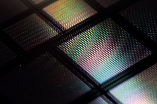
A close-up view of a new neuromorphic “brain-on-a-chip” that includes tens of thousands of memristors, or memory transistors. Credit: Peng Lin Courtesy: MIT
It’s hard to believe that a brain-on-a-chip might need sleep but that seems to be the case as far as the US Dept. of Energy’s Los Alamos National Laboratory is concerned. Before pursuing that line of thought, here’s some work from the Massachusetts Institute of Technology (MIT) involving memristors and a brain-on-a-chip. From a June 8, 2020 news item on ScienceDaily,
MIT engineers have designed a “brain-on-a-chip,” smaller than a piece of confetti, that is made from tens of thousands of artificial brain synapses known as memristors — silicon-based components that mimic the information-transmitting synapses in the human brain.
The researchers borrowed from principles of metallurgy to fabricate each memristor from alloys of silver and copper, along with silicon. When they ran the chip through several visual tasks, the chip was able to “remember” stored images and reproduce them many times over, in versions that were crisper and cleaner compared with existing memristor designs made with unalloyed elements.
Their results, published today in the journal Nature Nanotechnology, demonstrate a promising new memristor design for neuromorphic devices — electronics that are based on a new type of circuit that processes information in a way that mimics the brain’s neural architecture. Such brain-inspired circuits could be built into small, portable devices, and would carry out complex computational tasks that only today’s supercomputers can handle.
…
This ‘metallurgical’ approach differs somewhat from the protein nanowire approach used by the University of Massachusetts at Amherst team mentioned in my June 15, 2020 posting. Scientists are pursuing multiple pathways and we may find that we arrive with not ‘a single artificial brain but with many types of artificial brains.
“So far, artificial synapse networks exist as software. We’re trying to build real neural network hardware for portable artificial intelligence systems,” says Jeehwan Kim, associate professor of mechanical engineering at MIT. “Imagine connecting a neuromorphic device to a camera on your car, and having it recognize lights and objects and make a decision immediately, without having to connect to the internet. We hope to use energy-efficient memristors to do those tasks on-site, in real-time.”
Wandering ions
Memristors, or memory transistors [Note: Memristors are usually described as memory resistors; this is the first time I’ve seen ‘memory transistor’], are an essential element in neuromorphic computing. In a neuromorphic device, a memristor would serve as the transistor in a circuit, though its workings would more closely resemble a brain synapse — the junction between two neurons. The synapse receives signals from one neuron, in the form of ions, and sends a corresponding signal to the next neuron.
A transistor in a conventional circuit transmits information by switching between one of only two values, 0 and 1, and doing so only when the signal it receives, in the form of an electric current, is of a particular strength. In contrast, a memristor would work along a gradient, much like a synapse in the brain. The signal it produces would vary depending on the strength of the signal that it receives. This would enable a single memristor to have many values, and therefore carry out a far wider range of operations than binary transistors.
Like a brain synapse, a memristor would also be able to “remember” the value associated with a given current strength, and produce the exact same signal the next time it receives a similar current. This could ensure that the answer to a complex equation, or the visual classification of an object, is reliable — a feat that normally involves multiple transistors and capacitors.
Ultimately, scientists envision that memristors would require far less chip real estate than conventional transistors, enabling powerful, portable computing devices that do not rely on supercomputers, or even connections to the Internet.
Existing memristor designs, however, are limited in their performance. A single memristor is made of a positive and negative electrode, separated by a “switching medium,” or space between the electrodes. When a voltage is applied to one electrode, ions from that electrode flow through the medium, forming a “conduction channel” to the other electrode. The received ions make up the electrical signal that the memristor transmits through the circuit. The size of the ion channel (and the signal that the memristor ultimately produces) should be proportional to the strength of the stimulating voltage.
Kim says that existing memristor designs work pretty well in cases where voltage stimulates a large conduction channel, or a heavy flow of ions from one electrode to the other. But these designs are less reliable when memristors need to generate subtler signals, via thinner conduction channels.
The thinner a conduction channel, and the lighter the flow of ions from one electrode to the other, the harder it is for individual ions to stay together. Instead, they tend to wander from the group, disbanding within the medium. As a result, it’s difficult for the receiving electrode to reliably capture the same number of ions, and therefore transmit the same signal, when stimulated with a certain low range of current.
Borrowing from metallurgy
Kim and his colleagues found a way around this limitation by borrowing a technique from metallurgy, the science of melding metals into alloys and studying their combined properties.
“Traditionally, metallurgists try to add different atoms into a bulk matrix to strengthen materials, and we thought, why not tweak the atomic interactions in our memristor, and add some alloying element to control the movement of ions in our medium,” Kim says.
Engineers typically use silver as the material for a memristor’s positive electrode. Kim’s team looked through the literature to find an element that they could combine with silver to effectively hold silver ions together, while allowing them to flow quickly through to the other electrode.
The team landed on copper as the ideal alloying element, as it is able to bind both with silver, and with silicon.
“It acts as a sort of bridge, and stabilizes the silver-silicon interface,” Kim says.
To make memristors using their new alloy, the group first fabricated a negative electrode out of silicon, then made a positive electrode by depositing a slight amount of copper, followed by a layer of silver. They sandwiched the two electrodes around an amorphous silicon medium. In this way, they patterned a millimeter-square silicon chip with tens of thousands of memristors.
As a first test of the chip, they recreated a gray-scale image of the Captain America shield. They equated each pixel in the image to a corresponding memristor in the chip. They then modulated the conductance of each memristor that was relative in strength to the color in the corresponding pixel.
The chip produced the same crisp image of the shield, and was able to “remember” the image and reproduce it many times, compared with chips made of other materials.
The team also ran the chip through an image processing task, programming the memristors to alter an image, in this case of MIT’s Killian Court, in several specific ways, including sharpening and blurring the original image. Again, their design produced the reprogrammed images more reliably than existing memristor designs.
“We’re using artificial synapses to do real inference tests,” Kim says. “We would like to develop this technology further to have larger-scale arrays to do image recognition tasks. And some day, you might be able to carry around artificial brains to do these kinds of tasks, without connecting to supercomputers, the internet, or the cloud.”
Here’s a link to and a citation for the paper,
Alloying conducting channels for reliable neuromorphic computing by Hanwool Yeon, Peng Lin, Chanyeol Choi, Scott H. Tan, Yongmo Park, Doyoon Lee, Jaeyong Lee, Feng Xu, Bin Gao, Huaqiang Wu, He Qian, Yifan Nie, Seyoung Kim & Jeehwan Kim. Nature Nanotechnology (2020 DOI: https://doi.org/10.1038/s41565-020-0694-5 Published: 08 June 2020
This paper is behind a paywall.
Electric sheep and sleeping androids
I find it impossible to mention that androids might need sleep without reference to Philip K. Dick’s 1968 novel, “Do Androids Dream of Electric Sheep?”; its Wikipedia entry is here.
June 8, 2020
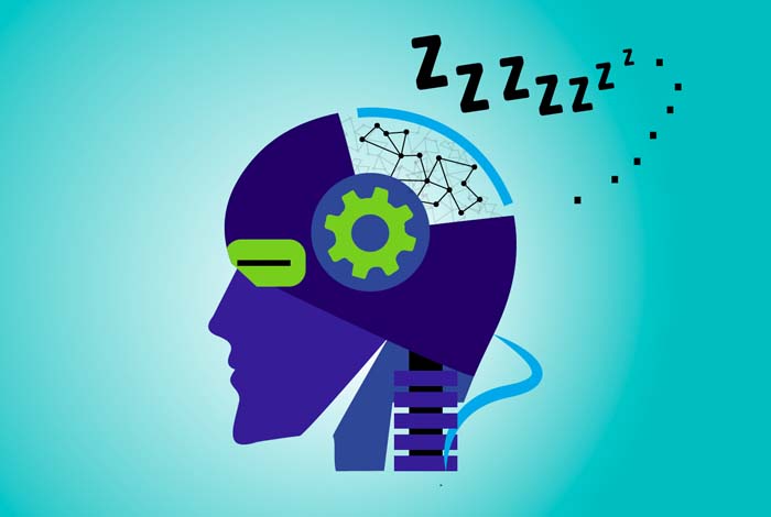
Intelligent machines of the future may need to sleep as much as we do.
Intelligent machines of the future may need to sleep as much as we do. Courtesy: Los Alamos National Laboratory
As it happens, I’m not the only one who felt the need to reference the novel, from a June 8, 2020 news item on ScienceDaily,
No one can say whether androids will dream of electric sheep, but they will almost certainly need periods of rest that offer benefits similar to those that sleep provides to living brains, according to new research from Los Alamos National Laboratory.
“We study spiking neural networks, which are systems that learn much as living brains do,” said Los Alamos National Laboratory computer scientist Yijing Watkins. “We were fascinated by the prospect of training a neuromorphic processor in a manner analogous to how humans and other biological systems learn from their environment during childhood development.”
Watkins and her research team found that the network simulations became unstable after continuous periods of unsupervised learning. When they exposed the networks to states that are analogous to the waves that living brains experience during sleep, stability was restored. “It was as though we were giving the neural networks the equivalent of a good night’s rest,” said Watkins.
The discovery came about as the research team worked to develop neural networks that closely approximate how humans and other biological systems learn to see. The group initially struggled with stabilizing simulated neural networks undergoing unsupervised dictionary training, which involves classifying objects without having prior examples to compare them to.
“The issue of how to keep learning systems from becoming unstable really only arises when attempting to utilize biologically realistic, spiking neuromorphic processors or when trying to understand biology itself,” said Los Alamos computer scientist and study coauthor Garrett Kenyon. “The vast majority of machine learning, deep learning, and AI researchers never encounter this issue because in the very artificial systems they study they have the luxury of performing global mathematical operations that have the effect of regulating the overall dynamical gain of the system.”
The researchers characterize the decision to expose the networks to an artificial analog of sleep as nearly a last ditch effort to stabilize them. They experimented with various types of noise, roughly comparable to the static you might encounter between stations while tuning a radio. The best results came when they used waves of so-called Gaussian noise, which includes a wide range of frequencies and amplitudes. They hypothesize that the noise mimics the input received by biological neurons during slow-wave sleep. The results suggest that slow-wave sleep may act, in part, to ensure that cortical neurons maintain their stability and do not hallucinate.
The groups’ next goal is to implement their algorithm on Intel’s Loihi neuromorphic chip. They hope allowing Loihi to sleep from time to time will enable it to stably process information from a silicon retina camera in real time. If the findings confirm the need for sleep in artificial brains, we can probably expect the same to be true of androids and other intelligent machines that may come about in the future.
Watkins will be presenting the research at the Women in Computer Vision Workshop on June 14 [2020] in Seattle.
The 2020 Women in Computer Vition Workshop (WICV) website is here. As is becoming standard practice for these times, the workshop was held in a virtual environment. Here’s a link to and a citation for the poster presentation paper,