Tag Archives: Tony F. Heinz

Courtesy of graphene: world’s thinnest light bulb

Columbia University’s (US) School of Engineering and Applied Science is trumpeting an achievement with graphene, i.e., the world’s thinnest light bulb. From a June 15, 2015 Columbia Engineering news release (also on EurekAlert),

Led by Young Duck Kim, a postdoctoral research scientist in James Hone’s group at Columbia Engineering, a team of scientists from Columbia, Seoul National University (SNU), and Korea Research Institute of Standards and Science (KRISS) reported today that they have demonstrated — for the first time — an on-chip visible light source using graphene, an atomically thin and perfectly crystalline form of carbon, as a filament. They attached small strips of graphene to metal electrodes, suspended the strips above the substrate, and passed a current through the filaments to cause them to heat up.

“We’ve created what is essentially the world’s thinnest light bulb,” says Hone, Wang Fon-Jen Professor of Mechanical Engineering at Columbia Engineering and coauthor of the study. “This new type of ‘broadband’ light emitter can be integrated into chips and will pave the way towards the realization of atomically thin, flexible, and transparent displays, and graphene-based on-chip optical communications.”

The news release goes on to describe some of the issues associated with generating light on a chip and how the researchers approached the problems (quick answer: they used graphene as the filament),

Creating light in small structures on the surface of a chip is crucial for developing fully integrated “photonic” circuits that do with light what is now done with electric currents in semiconductor integrated circuits. Researchers have developed many approaches to do this, but have not yet been able to put the oldest and simplest artificial light source—the incandescent light bulb—onto a chip. This is primarily because light bulb filaments must be extremely hot—thousands of degrees Celsius—in order to glow in the visible range and micro-scale metal wires cannot withstand such temperatures. In addition, heat transfer from the hot filament to its surroundings is extremely efficient at the microscale, making such structures impractical and leading to damage of the surrounding chip.

By measuring the spectrum of the light emitted from the graphene, the team was able to show that the graphene was reaching temperatures of above 2500 degrees Celsius, hot enough to glow brightly. “The visible light from atomically thin graphene is so intense that it is visible even to the naked eye, without any additional magnification,” explains Kim, first and co-lead author on the paper.

Interestingly, the spectrum of the emitted light showed peaks at specific wavelengths, which the team discovered was due to interference between the light emitted directly from the graphene and light reflecting off the silicon substrate and passing back through the graphene. Kim notes, “This is only possible because graphene is transparent, unlike any conventional filament, and allows us to tune the emission spectrum by changing the distance to the substrate.”

The ability of graphene to achieve such high temperatures without melting the substrate or the metal electrodes is due to another interesting property: as it heats up, graphene becomes a much poorer conductor of heat. This means that the high temperatures stay confined to a small “hot spot” in the center.

“At the highest temperatures, the electron temperature is much higher than that of acoustic vibrational modes of the graphene lattice, so that less energy is needed to attain temperatures needed for visible light emission,” Myung-Ho Bae, a senior researcher at KRISS and co-lead author, observes. “These unique thermal properties allow us to heat the suspended graphene up to half of the temperature of the sun, and improve efficiency 1000 times, as compared to graphene on a solid substrate.”

The team also demonstrated the scalability of their technique by realizing large-scale of arrays of chemical-vapor-deposited (CVD) graphene light emitters.

Yun Daniel Park, professor in the Department of Physics and Astronomy at Seoul National University and co-lead author, notes that they are working with the same material that Thomas Edison used when he invented the incandescent light bulb: “Edison originally used carbon as a filament for his light bulb and here we are going back to the same element, but using it in its pure form—graphene—and at its ultimate size limit—one atom thick.”

The group is currently working to further characterize the performance of these devices—for example, how fast they can be turned on and off to create “bits” for optical communications—and to develop techniques for integrating them into flexible substrates.

Hone adds, “We are just starting to dream about other uses for these structures—for example, as micro-hotplates that can be heated to thousands of degrees in a fraction of a second to study high-temperature chemical reactions or catalysis.”

Here’s a link to and a citation for the paper,

Bright visible light emission from graphene by Young Duck Kim, Hakseong Kim, Yujin Cho, Ji Hoon Ryoo, Cheol-Hwan Park, Pilkwang Kim, Yong Seung Kim, Sunwoo Lee, Yilei Li, Seung-Nam Park, Yong Shim Yoo, Duhee Yoon, Vincent E. Dorgan, Eric Pop, Tony F. Heinz, James Hone, Seung-Hyun Chun, Hyeonsik Cheong, Sang Wook Lee,    Myung-Ho Bae, & Yun Daniel Park. Nature Nanotechnology (2015) doi:10.1038/nnano.2015.118 Published online 15 June 2015

This paper is behind a paywall.

Two final notes: there was an announcement earlier this year (mentioned in my March 30, 2015 post) that a graphene light bulb would be in stores this year. Dexter Johnson notes in his June 15, 2015 post (Nanoclast blog on the IEEE [International Institute of Electrical and Electronics Engineers] website) that the earlier light bulb has a graphene coating. You may want to check out Dexter’s posting about the latest light bulb achievement as he also includes an embedded video illustrating how Columbia Engineering’s graphene filament works.
Bendable, stretchable, light-weight, and transparent: a new competitor in the competition for ‘thinnest electric generator’

An Oct. 15, 2014 Columbia University (New York, US) press release (also on EurekAlert), describes another contender for the title of the world’s thinnest electric generator,

Researchers from Columbia Engineering and the Georgia Institute of Technology [US] report today [Oct. 15, 2014] that they have made the first experimental observation of piezoelectricity and the piezotronic effect in an atomically thin material, molybdenum disulfide (MoS2), resulting in a unique electric generator and mechanosensation devices that are optically transparent, extremely light, and very bendable and stretchable.

In a paper published online October 15, 2014, in Nature, research groups from the two institutions demonstrate the mechanical generation of electricity from the two-dimensional (2D) MoS2 material. The piezoelectric effect in this material had previously been predicted theoretically.

Here’s a link to and a citation for the paper,

Piezoelectricity of single-atomic-layer MoS2 for energy conversion and piezotronics by Wenzhuo Wu, Lei Wang, Yilei Li, Fan Zhang, Long Lin, Simiao Niu, Daniel Chenet, Xian Zhang, Yufeng Hao, Tony F. Heinz, James Hone, & Zhong Lin Wang. Nature (2014) doi:10.1038/nature13792 Published online 15 October 2014

This paper is behind a paywall. There is a free preview available with ReadCube Access.

Getting back to the Columbia University press release, it offers a general description of piezoelectricity and some insight into this new research on molybdenum disulfide,

Piezoelectricity is a well-known effect in which stretching or compressing a material causes it to generate an electrical voltage (or the reverse, in which an applied voltage causes it to expand or contract). But for materials of only a few atomic thicknesses, no experimental observation of piezoelectricity has been made, until now. The observation reported today provides a new property for two-dimensional materials such as molybdenum disulfide, opening the potential for new types of mechanically controlled electronic devices.

“This material—just a single layer of atoms—could be made as a wearable device, perhaps integrated into clothing, to convert energy from your body movement to electricity and power wearable sensors or medical devices, or perhaps supply enough energy to charge your cell phone in your pocket,” says James Hone, professor of mechanical engineering at Columbia and co-leader of the research.

“Proof of the piezoelectric effect and piezotronic effect adds new functionalities to these two-dimensional materials,” says Zhong Lin Wang, Regents’ Professor in Georgia Tech’s School of Materials Science and Engineering and a co-leader of the research. “The materials community is excited about molybdenum disulfide, and demonstrating the piezoelectric effect in it adds a new facet to the material.”

Hone and his research group demonstrated in 2008 that graphene, a 2D form of carbon, is the strongest material. He and Lei Wang, a postdoctoral fellow in Hone’s group, have been actively exploring the novel properties of 2D materials like graphene and MoS2 as they are stretched and compressed.

Zhong Lin Wang and his research group pioneered the field of piezoelectric nanogenerators for converting mechanical energy into electricity. He and postdoctoral fellow Wenzhuo Wu are also developing piezotronic devices, which use piezoelectric charges to control the flow of current through the material just as gate voltages do in conventional three-terminal transistors.

There are two keys to using molybdenum disulfide for generating current: using an odd number of layers and flexing it in the proper direction. The material is highly polar, but, Zhong Lin Wang notes, so an even number of layers cancels out the piezoelectric effect. The material’s crystalline structure also is piezoelectric in only certain crystalline orientations.

For the Nature study, Hone’s team placed thin flakes of MoS2 on flexible plastic substrates and determined how their crystal lattices were oriented using optical techniques. They then patterned metal electrodes onto the flakes. In research done at Georgia Tech, Wang’s group installed measurement electrodes on samples provided by Hone’s group, then measured current flows as the samples were mechanically deformed. They monitored the conversion of mechanical to electrical energy, and observed voltage and current outputs.

The researchers also noted that the output voltage reversed sign when they changed the direction of applied strain, and that it disappeared in samples with an even number of atomic layers, confirming theoretical predictions published last year. The presence of piezotronic effect in odd layer MoS2 was also observed for the first time.

“What’s really interesting is we’ve now found that a material like MoS2, which is not piezoelectric in bulk form, can become piezoelectric when it is thinned down to a single atomic layer,” says Lei Wang.

To be piezoelectric, a material must break central symmetry. A single atomic layer of MoS2 has such a structure, and should be piezoelectric. However, in bulk MoS2, successive layers are oriented in opposite directions, and generate positive and negative voltages that cancel each other out and give zero net piezoelectric effect.

“This adds another member to the family of piezoelectric materials for functional devices,” says Wenzhuo Wu.

In fact, MoS2 is just one of a group of 2D semiconducting materials known as transition metal dichalcogenides, all of which are predicted to have similar piezoelectric properties. These are part of an even larger family of 2D materials whose piezoelectric materials remain unexplored. Importantly, as has been shown by Hone and his colleagues, 2D materials can be stretched much farther than conventional materials, particularly traditional ceramic piezoelectrics, which are quite brittle.

The research could open the door to development of new applications for the material and its unique properties.

“This is the first experimental work in this area and is an elegant example of how the world becomes different when the size of material shrinks to the scale of a single atom,” Hone adds. “With what we’re learning, we’re eager to build useful devices for all kinds of applications.”

Ultimately, Zhong Lin Wang notes, the research could lead to complete atomic-thick nanosystems that are self-powered by harvesting mechanical energy from the environment. This study also reveals the piezotronic effect in two-dimensional materials for the first time, which greatly expands the application of layered materials for human-machine interfacing, robotics, MEMS, and active flexible electronics.

I see there’s a reference in that last paragraph to “harvesting mechanical energy from  the environment.” I’m not sure what they mean by that but I have written a few times about harvesting biomechanical energy. One of my earliest pieces is a July 12, 2010 post which features work by Zhong Lin Wang on harvesting energy from heart beats, blood flow, muscle stretching, or even irregular vibrations. One of my latest pieces is a Sept. 17, 2014 post about some work in Canada on harvesting energy from the jaw as you chew.

A final note, Dexter Johnson discusses this work in an Oct. 16, 2014 post on the Nanoclast blog (on the IEEE [Institute of Electrical and Electronics Engineers] website).

Graphene euphoria, heat sinks, diamonds, and Rice University’s Ajayan Group

Pulickel Ajayan, at Rice University (Texas), must have one of the most active laboratories in the US where nanotechnology-based research and announcements about it are concerned and I imagine it’s an exciting place to work. Whoever wrote the May 28, 2013 Rice University news release on EurekAlert seems to have caught some of the Ajayan Group’s excitement,

What may be the ultimate heat sink is only possible because of yet another astounding capability of graphene. The one-atom-thick form of carbon can act as a go-between that allows vertically aligned carbon nanotubes to grow on nearly anything.

That includes diamonds. A diamond film/graphene/nanotube structure was one result of new research carried out by scientists at Rice University and the Honda Research Institute USA, reported today in Nature’s online journal Scientific Reports.

The heart of the research is the revelation that when graphene is used as a middleman, surfaces considered unusable as substrates for carbon nanotube growth now have the potential to do so. Diamond happens to be a good example, according to Rice materials scientist Pulickel Ajayan and Honda chief scientist Avetik Harutyunyan.

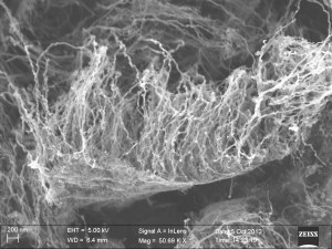
Here’s an image the team has provided,

Rice University and the Honda Research Institute use single-layer graphene to grow forests of nanotubes on virtually anything. The image shows freestanding carbon nanotubes on graphene that has been lifted off of a quartz substrate. One hybrid material created by the labs combines three allotropes of carbon – graphene, nanotubes and diamond – into a superior material for thermal management. (Credit: Honda Research Institute)

Rice University and the Honda Research Institute use single-layer graphene to grow forests of nanotubes on virtually anything. The image shows freestanding carbon nanotubes on graphene that has been lifted off of a quartz substrate. One hybrid material created by the labs combines three allotropes of carbon – graphene, nanotubes and diamond – into a superior material for thermal management. (Credit: Honda Research Institute)

The news release provides more information about the diamond-carbon nanotube-graphene hybrid material,

Diamond conducts heat very well, five times better than copper. But its available surface area is very low. By its very nature, one-atom-thick graphene is all surface area. The same could be said of carbon nanotubes, which are basically rolled-up tubes of graphene. A vertically aligned forest of carbon nanotubes grown on diamond would disperse heat like a traditional heat sink, but with millions of fins. Such an ultrathin array could save space in small microprocessor-based devices.

“Further work along these lines could produce such structures as patterned nanotube arrays on diamond that could be utilized in electronic devices,” Ajayan said. Graphene and metallic nanotubes are also highly conductive; in combination with metallic substrates, they may also have uses in advanced electronics, he said.

To test their ideas, the Honda team grew various types of graphene on copper foil by standard chemical vapor deposition. They then transferred the tiny graphene sheets to diamond, quartz and other metals for further study by the Rice team.

They found that only single-layer graphene worked well, and sheets with ripples or wrinkles worked best. The defects appeared to capture and hold the airborne iron-based catalyst particles from which the nanotubes grow. The researchers think graphene facilitates nanotube growth by keeping the catalyst particles from clumping.

Ajayan thinks the extreme thinness of graphene does the trick. In a previous study, the Rice lab found graphene shows materials coated with graphene can get wet, but the graphene provides protection against oxidation. “That might be one of the big things about graphene, that you can have a noninvasive coating that keeps the property of the substrate but adds value,” he said. “Here it allows the catalytic activity but stops the catalyst from aggregating.”

Testing found that the graphene layer remains intact between the nanotube forest and the diamond or other substrate. On a metallic substrate like copper, the entire hybrid is highly conductive.

Such seamless integration through the graphene interface would provide low-contact resistance between current collectors and the active materials of electrochemical cells, a remarkable step toward building high-power energy devices, said Rice research scientist and co-author Leela Mohana Reddy Arava.

Here’s a link to and a citation for the paper,

Graphene as an atomically thin interface for growth of vertically aligned carbon nanotubes by Rahul Rao, Gugang Chen, Leela Mohana Reddy Arava, Kaushik Kalaga, Masahiro Ishigami, Tony F. Heinz, Pulickel M. Ajayan, & Avetik R. Harutyunyan. Scientific Reports 3, Article number: 1891 doi:10.1038/srep01891 Published 28 May 2013

Scientific Reports, a Nature publication, provides open access to its papers.