Over 30 years in the dreaming, the International Thermonuclear Experimental Reactor (ITER) is now said to be 1/2 way to completing construction. A December 6, 2017 ITER press release (received via email) makes the joyful announcement,
WORLD’S MOST COMPLEX MACHINE IS 50 PERCENT COMPLETED
ITER is proving that fusion is the future source of clean, abundant, safe and economic energy_
The International Thermonuclear Experimental Reactor (ITER), a project to prove that fusion power can be produced on a commercial scale and is sustainable, is now 50 percent built to initial operation. Fusion is the same energy source from the Sun that gives the Earth its light and warmth.
ITER will use hydrogen fusion, controlled by superconducting magnets, to produce massive heat energy. In the commercial machines that will follow, this heat will drive turbines to produce electricity with these positive benefits:
* Fusion energy is carbon-free and environmentally sustainable, yet much more powerful than fossil fuels. A pineapple-sized amount of hydrogen offers as much fusion energy as 10,000 tons of coal.
* ITER uses two forms of hydrogen fuel: deuterium, which is easily extracted from seawater; and tritium, which is bred from lithium inside the fusion reactor. The supply of fusion fuel for industry and megacities is abundant, enough for millions of years.
* When the fusion reaction is disrupted, the reactor simply shuts down-safely and without external assistance. Tiny amounts of fuel are used, about 2-3 grams at a time; so there is no physical possibility of a meltdown accident.
* Building and operating a fusion power plant is targeted to be comparable to the cost of a fossil fuel or nuclear fission plant. But unlike today’s nuclear plants, a fusion plant will not have the costs of high-level radioactive waste disposal. And unlike fossil fuel plants,
fusion will not have the environmental cost of releasing CO2 and other pollutants.
ITER is the most complex science project in human history. The hydrogen plasma will be heated to 150 million degrees Celsius, ten times hotter than the core of the Sun, to enable the fusion reaction. The process happens in a donut-shaped reactor, called a tokamak(*), which is surrounded by giant magnets that confine and circulate the superheated, ionized plasma, away from the metal walls. The superconducting magnets must be cooled to minus 269°C, as cold as interstellar space.
The ITER facility is being built in Southern France by a scientific partnership of 35 countries. ITER’s specialized components, roughly 10 million parts in total, are being manufactured in industrial facilities all over the world. They are subsequently shipped to the ITER worksite, where they must be assembled, piece-by-piece, into the final machine.
Each of the seven ITER members-the European Union, China, India, Japan, Korea, Russia, and the United States-is fabricating a significant portion of the machine. This adds to ITER’s complexity.
In a message dispatched on December 1 [2017] to top-level officials in ITER member governments, the ITER project reported that it had completed 50 percent of the “total construction work scope through First Plasma” (**). First Plasma, scheduled for December 2025, will be the first stage of operation for ITER as a functional machine.
“The stakes are very high for ITER,” writes Bernard Bigot, Ph.D., Director-General of ITER. “When we prove that fusion is a viable energy source, it will eventually replace burning fossil fuels, which are non-renewable and non-sustainable. Fusion will be complementary with wind, solar, and other renewable energies.
“ITER’s success has demanded extraordinary project management, systems engineering, and almost perfect integration of our work.
“Our design has taken advantage of the best expertise of every member’s scientific and industrial base. No country could do this alone. We are all learning from each other, for the world’s mutual benefit.”
The ITER 50 percent milestone is getting significant attention.
“We are fortunate that ITER and fusion has had the support of world leaders, historically and currently,” says Director-General Bigot. “The concept of the ITER project was conceived at the 1985 Geneva Summit between Ronald Reagan and Mikhail Gorbachev. When the ITER Agreement was signed in 2006, it was strongly supported by leaders such as French President Jacques Chirac, U.S. President George W. Bush, and Indian Prime Minister Manmohan Singh.
“More recently, President Macron and U.S. President Donald Trump exchanged letters about ITER after their meeting this past July. One month earlier, President Xi Jinping of China hosted Russian President Vladimir Putin and other world leaders in a showcase featuring ITER and fusion power at the World EXPO in Astana, Kazakhstan.
“We know that other leaders have been similarly involved behind the scenes. It is clear that each ITER member understands the value and importance of this project.”
Why use this complex manufacturing arrangement?
More than 80 percent of the cost of ITER, about $22 billion or EUR18 billion, is contributed in the form of components manufactured by the partners. Many of these massive components of the ITER machine must be precisely fitted-for example, 17-meter-high magnets with less than a millimeter of tolerance. Each component must be ready on time to fit into the Master Schedule for machine assembly.
Members asked for this deal for three reasons. First, it means that most of the ITER costs paid by any member are actually paid to that member’s companies; the funding stays in-country. Second, the companies working on ITER build new industrial expertise in major fields-such as electromagnetics, cryogenics, robotics, and materials science. Third, this new expertise leads to innovation and spin-offs in other fields.
For example, expertise gained working on ITER’s superconducting magnets is now being used to map the human brain more precisely than ever before.
The European Union is paying 45 percent of the cost; China, India, Japan, Korea, Russia, and the United States each contribute 9 percent equally. All members share in ITER’s technology; they receive equal access to the intellectual property and innovation that comes from building ITER.
When will commercial fusion plants be ready?
ITER scientists predict that fusion plants will start to come on line as soon as 2040. The exact timing, according to fusion experts, will depend on the level of public urgency and political will that translates to financial investment.
How much power will they provide?
The ITER tokamak will produce 500 megawatts of thermal power. This size is suitable for studying a “burning” or largely self-heating plasma, a state of matter that has never been produced in a controlled environment on Earth. In a burning plasma, most of the plasma heating comes from the fusion reaction itself. Studying the fusion science and technology at ITER’s scale will enable optimization of the plants that follow.
A commercial fusion plant will be designed with a slightly larger plasma chamber, for 10-15 times more electrical power. A 2,000-megawatt fusion electricity plant, for example, would supply 2 million homes.
How much would a fusion plant cost and how many will be needed?
The initial capital cost of a 2,000-megawatt fusion plant will be in the range of $10 billion. These capital costs will be offset by extremely low operating costs, negligible fuel costs, and infrequent component replacement costs over the 60-year-plus life of the plant. Capital costs will decrease with large-scale deployment of fusion plants.
At current electricity usage rates, one fusion plant would be more than enough to power a city the size of Washington, D.C. The entire D.C. metropolitan area could be powered with four fusion plants, with zero carbon emissions.
“If fusion power becomes universal, the use of electricity could be expanded greatly, to reduce the greenhouse gas emissions from transportation, buildings and industry,” predicts Dr. Bigot. “Providing clean, abundant, safe, economic energy will be a miracle for our planet.”
* * *
FOOTNOTES:
* “Tokamak” is a word of Russian origin meaning a toroidal or donut-shaped magnetic chamber. Tokamaks have been built and operated for the past six decades. They are today’s most advanced fusion device design.
** “Total construction work scope,” as used in ITER’s project performance metrics, includes design, component manufacturing, building construction, shipping and delivery, assembly, and installation.
It is an extraordinary project on many levels as Henry Fountain notes in a March 27, 2017 article for the New York Times (Note: Links have been removed),
At a dusty construction site here amid the limestone ridges of Provence, workers scurry around immense slabs of concrete arranged in a ring like a modern-day Stonehenge.
It looks like the beginnings of a large commercial power plant, but it is not. The project, called ITER, is an enormous, and enormously complex and costly, physics experiment. But if it succeeds, it could determine the power plants of the future and make an invaluable contribution to reducing planet-warming emissions.
ITER, short for International Thermonuclear Experimental Reactor (and pronounced EAT-er), is being built to test a long-held dream: that nuclear fusion, the atomic reaction that takes place in the sun and in hydrogen bombs, can be controlled to generate power.
…
ITER will produce heat, not electricity. But if it works — if it produces more energy than it consumes, which smaller fusion experiments so far have not been able to do — it could lead to plants that generate electricity without the climate-affecting carbon emissions of fossil-fuel plants or most of the hazards of existing nuclear reactors that split atoms rather than join them.
Success, however, has always seemed just a few decades away for ITER. The project has progressed in fits and starts for years, plagued by design and management problems that have led to long delays and ballooning costs.
ITER is moving ahead now, with a director-general, Bernard Bigot, who took over two years ago after an independent analysis that was highly critical of the project. Dr. Bigot, who previously ran France’s atomic energy agency, has earned high marks for resolving management problems and developing a realistic schedule based more on physics and engineering and less on politics.
…
The site here is now studded with tower cranes as crews work on the concrete structures that will support and surround the heart of the experiment, a doughnut-shaped chamber called a tokamak. This is where the fusion reactions will take place, within a plasma, a roiling cloud of ionized atoms so hot that it can be contained only by extremely strong magnetic fields.
Here’s a rendering of the proposed reactor,
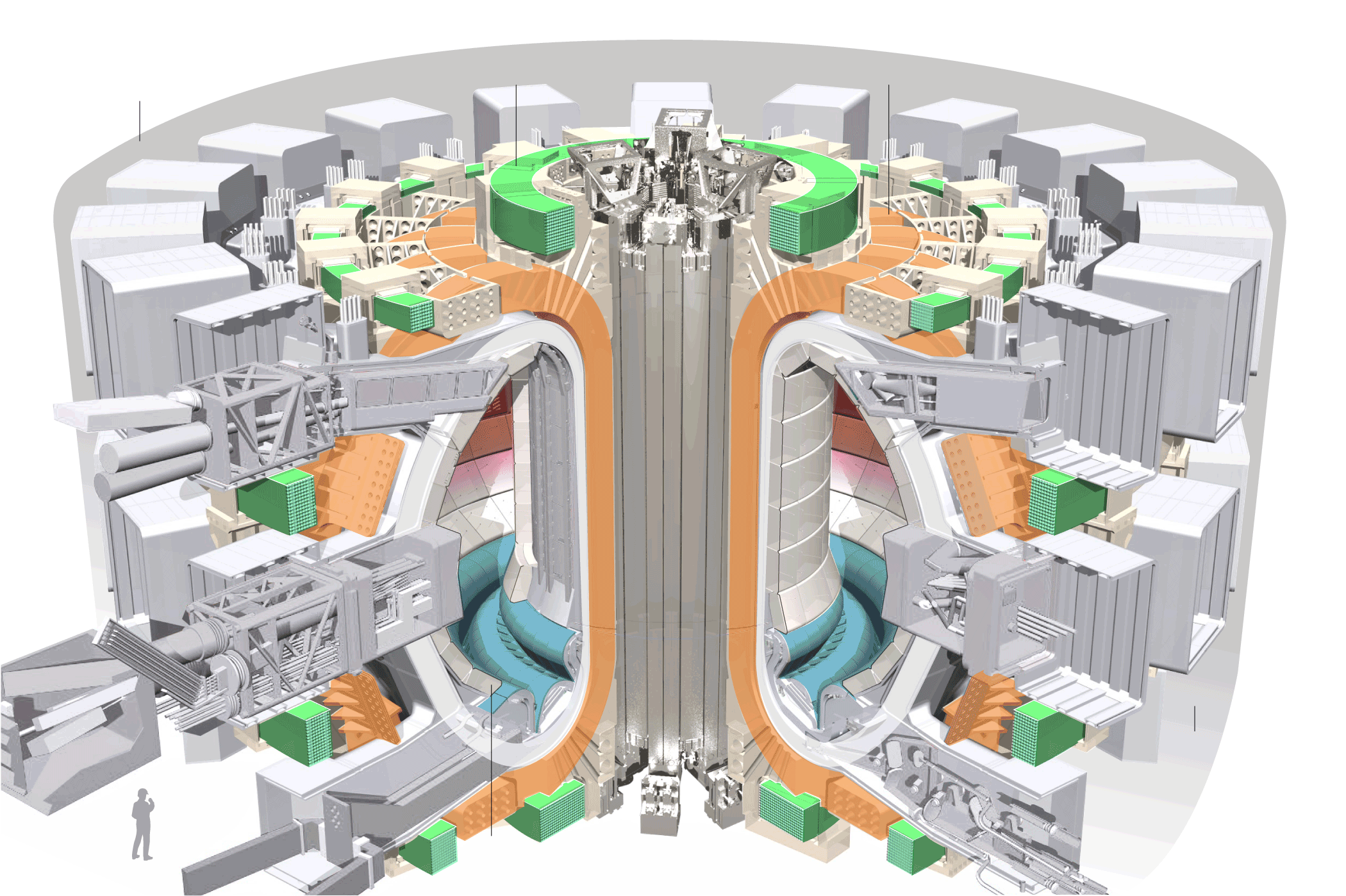
Source: ITER Organization
It seems the folks at the New York Times decided to remove the notes which help make sense of this image. However, it does get the idea across.
If I read the article rightly, the official cost in March 2017 was around 22 B Euros and more will likely be needed. You can read Fountain’s article for more information about fusion and ITER or go to the ITER website.
I could have sworn a local (Vancouver area) company called General Fusion was involved in the ITER project but I can’t track down any sources for confirmation. The sole connection I could find is in a documentary about fusion technology,
Here’s a little context for the film from a July 4, 2017 General Fusion news release (Note: A link has been removed),
A new documentary featuring General Fusion has captured the exciting progress in fusion across the public and private sectors.
Let There Be Light made its international premiere at the South By Southwest (SXSW) music and film festival in March [2017] to critical acclaim. The film was quickly purchased by Amazon Video, where it will be available for more than 70 million users to stream.
Let There Be Light follows scientists at General Fusion, ITER and Lawrenceville Plasma Physics in their pursuit of a clean, safe and abundant source of energy to power the world.
The feature length documentary has screened internationally across Europe and North America. Most recently it was shown at the Hot Docs film festival in Toronto, where General Fusion founder and Chief Scientist Dr. Michel Laberge joined fellow fusion physicist Dr. Mark Henderson from ITER at a series of Q&A panels with the filmmakers.
Laberge and Henderson were also interviewed by the popular CBC radio science show Quirks and Quarks, discussing different approaches to fusion, its potential benefits, and the challenges it faces.
It is yet to be confirmed when the film will be release for streaming, check Amazon Video for details.
You can find out more about General Fusion here.
Brief final comment
ITER is a breathtaking effort but if you’ve read about other large scale projects such as building a railway across the Canadian Rocky Mountains, establishing telecommunications in an astonishing number of countries around the world, getting someone to the moon, eliminating small pox, building the pyramids, etc., it seems standard operating procedure both for the successes I’ve described and for the failures we’ve forgotten. Where ITER will finally rest on the continuum between success and failure is yet to be determined but the problems experienced so far are not necessarily a predictor.
I wish the engineers, scientists, visionaries, and others great success with finding better ways to produce energy.