Tag Archives: Han Wang

100-fold increase in AI energy efficiency

Most people don’t realize how much energy computing, streaming video, and other technologies consume and AI (artificial intelligence) consumes a lot. (For more about work being done in this area, there’s my October 13, 2023 posting about an upcoming ArtSci Salon event in Toronto featuring Laura U. Marks’s recent work ‘Streaming Carbon Footprint’ and my October 16, 2023 posting about how much water is used for AI.)

So this news is welcome, from an October 12, 2023 Northwestern University news release (also received via email and on EurekAlert), Note: Links have been removed,

AI just got 100-fold more energy efficient

Nanoelectronic device performs real-time AI classification without relying on the cloud

– AI is so energy hungry that most data analysis must be performed in the cloud
– New energy-efficient device enables AI tasks to be performed within wearables
– This allows real-time analysis and diagnostics for faster medical interventions
– Researchers tested the device by classifying 10,000 electrocardiogram samples
– The device successfully identified six types of heart beats with 95% accuracy

Northwestern University engineers have developed a new nanoelectronic device that can perform accurate machine-learning classification tasks in the most energy-efficient manner yet. Using 100-fold less energy than current technologies, the device can crunch large amounts of data and perform artificial intelligence (AI) tasks in real time without beaming data to the cloud for analysis.

With its tiny footprint, ultra-low power consumption and lack of lag time to receive analyses, the device is ideal for direct incorporation into wearable electronics (like smart watches and fitness trackers) for real-time data processing and near-instant diagnostics.

To test the concept, engineers used the device to classify large amounts of information from publicly available electrocardiogram (ECG) datasets. Not only could the device efficiently and correctly identify an irregular heartbeat, it also was able to determine the arrhythmia subtype from among six different categories with near 95% accuracy.

The research was published today (Oct. 12 [2023]) in the journal Nature Electronics.

“Today, most sensors collect data and then send it to the cloud, where the analysis occurs on energy-hungry servers before the results are finally sent back to the user,” said Northwestern’s Mark C. Hersam, the study’s senior author. “This approach is incredibly expensive, consumes significant energy and adds a time delay. Our device is so energy efficient that it can be deployed directly in wearable electronics for real-time detection and data processing, enabling more rapid intervention for health emergencies.”

A nanotechnology expert, Hersam is Walter P. Murphy Professor of Materials Science and Engineering at Northwestern’s McCormick School of Engineering. He also is chair of the Department of Materials Science and Engineering, director of the Materials Research Science and Engineering Center and member of the International Institute of Nanotechnology. Hersam co-led the research with Han Wang, a professor at the University of Southern California, and Vinod Sangwan, a research assistant professor at Northwestern.

Before machine-learning tools can analyze new data, these tools must first accurately and reliably sort training data into various categories. For example, if a tool is sorting photos by color, then it needs to recognize which photos are red, yellow or blue in order to accurately classify them. An easy chore for a human, yes, but a complicated — and energy-hungry — job for a machine.

For current silicon-based technologies to categorize data from large sets like ECGs, it takes more than 100 transistors — each requiring its own energy to run. But Northwestern’s nanoelectronic device can perform the same machine-learning classification with just two devices. By reducing the number of devices, the researchers drastically reduced power consumption and developed a much smaller device that can be integrated into a standard wearable gadget.

The secret behind the novel device is its unprecedented tunability, which arises from a mix of materials. While traditional technologies use silicon, the researchers constructed the miniaturized transistors from two-dimensional molybdenum disulfide and one-dimensional carbon nanotubes. So instead of needing many silicon transistors — one for each step of data processing — the reconfigurable transistors are dynamic enough to switch among various steps.

“The integration of two disparate materials into one device allows us to strongly modulate the current flow with applied voltages, enabling dynamic reconfigurability,” Hersam said. “Having a high degree of tunability in a single device allows us to perform sophisticated classification algorithms with a small footprint and low energy consumption.”

To test the device, the researchers looked to publicly available medical datasets. They first trained the device to interpret data from ECGs, a task that typically requires significant time from trained health care workers. Then, they asked the device to classify six types of heart beats: normal, atrial premature beat, premature ventricular contraction, paced beat, left bundle branch block beat and right bundle branch block beat.

The nanoelectronic device was able to identify accurately each arrhythmia type out of 10,000 ECG samples. By bypassing the need to send data to the cloud, the device not only saves critical time for a patient but also protects privacy.

“Every time data are passed around, it increases the likelihood of the data being stolen,” Hersam said. “If personal health data is processed locally — such as on your wrist in your watch — that presents a much lower security risk. In this manner, our device improves privacy and reduces the risk of a breach.”

Hersam imagines that, eventually, these nanoelectronic devices could be incorporated into everyday wearables, personalized to each user’s health profile for real-time applications. They would enable people to make the most of the data they already collect without sapping power.

“Artificial intelligence tools are consuming an increasing fraction of the power grid,” Hersam said. “It is an unsustainable path if we continue relying on conventional computer hardware.”

Here’s a link to and a citation for the paper,

Reconfigurable mixed-kernel heterojunction transistors for personalized support vector machine classification by Xiaodong Yan, Justin H. Qian, Jiahui Ma, Aoyang Zhang, Stephanie E. Liu, Matthew P. Bland, Kevin J. Liu, Xuechun Wang, Vinod K. Sangwan, Han Wang & Mark C. Hersam. Nature Electronics (2023) DOI: https://doi.org/10.1038/s41928-023-01042-7 Published: 12 October 2023

This paper is behind a paywall.
Combining silicon with metal oxide memristors to create powerful, low-energy intensive chips enabling AI in portable devices

In this one week, I’m publishing my first stories (see also June 13, 2023 posting “ChatGPT and a neuromorphic [brainlike] synapse“) where artificial intelligence (AI) software is combined with a memristor (hardware component) for brainlike (neuromorphic) computing.

Here’s more about some of the latest research from a March 30, 2023 news item on ScienceDaily,

Everyone is talking about the newest AI and the power of neural networks, forgetting that software is limited by the hardware on which it runs. But it is hardware, says USC [University of Southern California] Professor of Electrical and Computer Engineering Joshua Yang, that has become “the bottleneck.” Now, Yang’s new research with collaborators might change that. They believe that they have developed a new type of chip with the best memory of any chip thus far for edge AI (AI in portable devices).

A March 29, 2023 University of Southern California (USC) news release (also on EurekAlert), which originated the news item, contextualizes the research and delves further into the topic of neuromorphic hardware,

For approximately the past 30 years, while the size of the neural networks needed for AI and data science applications doubled every 3.5 months, the hardware capability needed to process them doubled only every 3.5 years. According to Yang, hardware presents a more and more severe problem for which few have patience. 

Governments, industry, and academia are trying to address this hardware challenge worldwide. Some continue to work on hardware solutions with silicon chips, while others are experimenting with new types of materials and devices.  Yang’s work falls into the middle—focusing on exploiting and combining the advantages of the new materials and traditional silicon technology that could support heavy AI and data science computation. 

Their new paper in Nature focuses on the understanding of fundamental physics that leads to a drastic increase in memory capacity needed for AI hardware. The team led by Yang, with researchers from USC (including Han Wang’s group), MIT [Massachusetts Institute of Technology], and the University of Massachusetts, developed a protocol for devices to reduce “noise” and demonstrated the practicality of using this protocol in integrated chips. This demonstration was made at TetraMem, a startup company co-founded by Yang and his co-authors  (Miao Hu, Qiangfei Xia, and Glenn Ge), to commercialize AI acceleration technology. According to Yang, this new memory chip has the highest information density per device (11 bits) among all types of known memory technologies thus far. Such small but powerful devices could play a critical role in bringing incredible power to the devices in our pockets. The chips are not just for memory but also for the processor. And millions of them in a small chip, working in parallel to rapidly run your AI tasks, could only require a small battery to power it. 

The chips that Yang and his colleagues are creating combine silicon with metal oxide memristors in order to create powerful but low-energy intensive chips. The technique focuses on using the positions of atoms to represent information rather than the number of electrons (which is the current technique involved in computations on chips). The positions of the atoms offer a compact and stable way to store more information in an analog, instead of digital fashion. Moreover, the information can be processed where it is stored instead of being sent to one of the few dedicated ‘processors,’ eliminating the so-called ‘von Neumann bottleneck’ existing in current computing systems.  In this way, says Yang, computing for AI is “more energy efficient with a higher throughput.”

How it works: 

Yang explains that electrons which are manipulated in traditional chips, are “light.” And this lightness, makes them prone to moving around and being more volatile.  Instead of storing memory through electrons, Yang and collaborators are storing memory in full atoms. Here is why this memory matters. Normally, says Yang, when one turns off a computer, the information memory is gone—but if you need that memory to run a new computation and your computer needs the information all over again, you have lost both time and energy.  This new method, focusing on activating atoms rather than electrons, does not require battery power to maintain stored information. Similar scenarios happen in AI computations, where a stable memory capable of high information density is crucial. Yang imagines this new tech that may enable powerful AI capability in edge devices, such as Google Glasses, which he says previously suffered from a frequent recharging issue.

Further, by converting chips to rely on atoms as opposed to electrons, chips become smaller.  Yang adds that with this new method, there is more computing capacity at a smaller scale. And this method, he says, could offer “many more levels of memory to help increase information density.” 

To put it in context, right now, ChatGPT is running on a cloud. The new innovation, followed by some further development, could put the power of a mini version of ChatGPT in everyone’s personal device. It could make such high-powered tech more affordable and accessible for all sorts of applications. 

Here’s a link to and a citation for the paper,

Thousands of conductance levels in memristors integrated on CMOS by Mingyi Rao, Hao Tang, Jiangbin Wu, Wenhao Song, Max Zhang, Wenbo Yin, Ye Zhuo, Fatemeh Kiani, Benjamin Chen, Xiangqi Jiang, Hefei Liu, Hung-Yu Chen, Rivu Midya, Fan Ye, Hao Jiang, Zhongrui Wang, Mingche Wu, Miao Hu, Han Wang, Qiangfei Xia, Ning Ge, Ju Li & J. Joshua Yang. Nature volume 615, pages 823–829 (2023) DOI: https://doi.org/10.1038/s41586-023-05759-5 Issue Date: 30 March 2023 Published: 29 March 2023

This paper is behind a paywall.

Two approaches to memristors

Within one day of each other in October 2018, two different teams working on memristors with applications to neuroprosthetics and neuromorphic computing (brainlike computing) announced their results.

Russian team

An October 15, 2018 (?) Lobachevsky University press release (also published on October 15, 2018 on EurekAlert) describes a new approach to memristors,

Biological neurons are coupled unidirectionally through a special junction called a synapse. An electrical signal is transmitted along a neuron after some biochemical reactions initiate a chemical release to activate an adjacent neuron. These junctions are crucial for cognitive functions, such as perception, learning and memory.

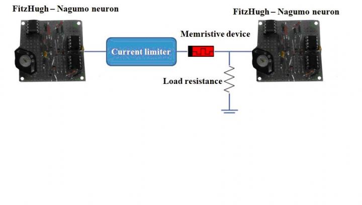
A group of researchers from Lobachevsky University in Nizhny Novgorod investigates the dynamics of an individual memristive device when it receives a neuron-like signal as well as the dynamics of a network of analog electronic neurons connected by means of a memristive device. According to Svetlana Gerasimova, junior researcher at the Physics and Technology Research Institute and at the Neurotechnology Department of Lobachevsky University, this system simulates the interaction between synaptically coupled brain neurons while the memristive device imitates a neuron axon.

A memristive device is a physical model of Chua’s [Dr. Leon Chua, University of California at Berkeley; see my May 9, 2008 posting for a brief description Dr. Chua’s theory] memristor, which is an electric circuit element capable of changing its resistance depending on the electric signal received at the input. The device based on a Au/ZrO2(Y)/TiN/Ti structure demonstrates reproducible bipolar switching between the low and high resistance states. Resistive switching is determined by the oxidation and reduction of segments of conducting channels (filaments) in the oxide film when voltage with different polarity is applied to it. In the context of the present work, the ability of a memristive device to change conductivity under the action of pulsed signals makes it an almost ideal electronic analog of a synapse.

Lobachevsky University scientists and engineers supported by the Russian Science Foundation (project No.16-19-00144) have experimentally implemented and theoretically described the synaptic connection of neuron-like generators using the memristive interface and investigated the characteristics of this connection.

“Each neuron is implemented in the form of a pulse signal generator based on the FitzHugh-Nagumo model. This model provides a qualitative description of the main neurons’ characteristics: the presence of the excitation threshold, the presence of excitable and self-oscillatory regimes with the possibility of a changeover. At the initial time moment, the master generator is in the self-oscillatory mode, the slave generator is in the excitable mode, and the memristive device is used as a synapse. The signal from the master generator is conveyed to the input of the memristive device, the signal from the output of the memristive device is transmitted to the input of the slave generator via the loading resistance. When the memristive device switches from a high resistance to a low resistance state, the connection between the two neuron-like generators is established. The master generator goes into the oscillatory mode and the signals of the generators are synchronized. Different signal modulation mode synchronizations were demonstrated for the Au/ZrO2(Y)/TiN/Ti memristive device,” – says Svetlana Gerasimova.

UNN researchers believe that the next important stage in the development of neuromorphic systems based on memristive devices is to apply such systems in neuroprosthetics. Memristive systems will provide a highly efficient imitation of synaptic connection due to the stochastic nature of the memristive phenomenon and can be used to increase the flexibility of the connections for neuroprosthetic purposes. Lobachevsky University scientists have vast experience in the development of neurohybrid systems. In particular, a series of experiments was performed with the aim of connecting the FitzHugh-Nagumo oscillator with a biological object, a rat brain hippocampal slice. The signal from the electronic neuron generator was transmitted through the optic fiber communication channel to the bipolar electrode which stimulated Schaffer collaterals (axons of pyramidal neurons in the CA3 field) in the hippocampal slices. “We are going to combine our efforts in the design of artificial neuromorphic systems and our experience of working with living cells to improve flexibility of prosthetics,” concludes S. Gerasimova.

The results of this research were presented at the 38th International Conference on Nonlinear Dynamics (Dynamics Days Europe) at Loughborough University (Great Britain).

This diagram illustrates an aspect of the work,

Caption: Schematic of electronic neurons coupling via a memristive device. Credit: Lobachevsky University

US team

The American Institute of Physics (AIP) announced the publication of a ‘memristor paper’ by a team from the University of Southern California (USC) in an October 16, 2018 news item on phys.org,

Just like their biological counterparts, hardware that mimics the neural circuitry of the brain requires building blocks that can adjust how they synapse, with some connections strengthening at the expense of others. One such approach, called memristors, uses current resistance to store this information. New work looks to overcome reliability issues in these devices by scaling memristors to the atomic level.

An October 16, 2018 AIP news release (also on EurekAlert), which originated the news item, delves further into the particulars of this particular piece of memristor research,

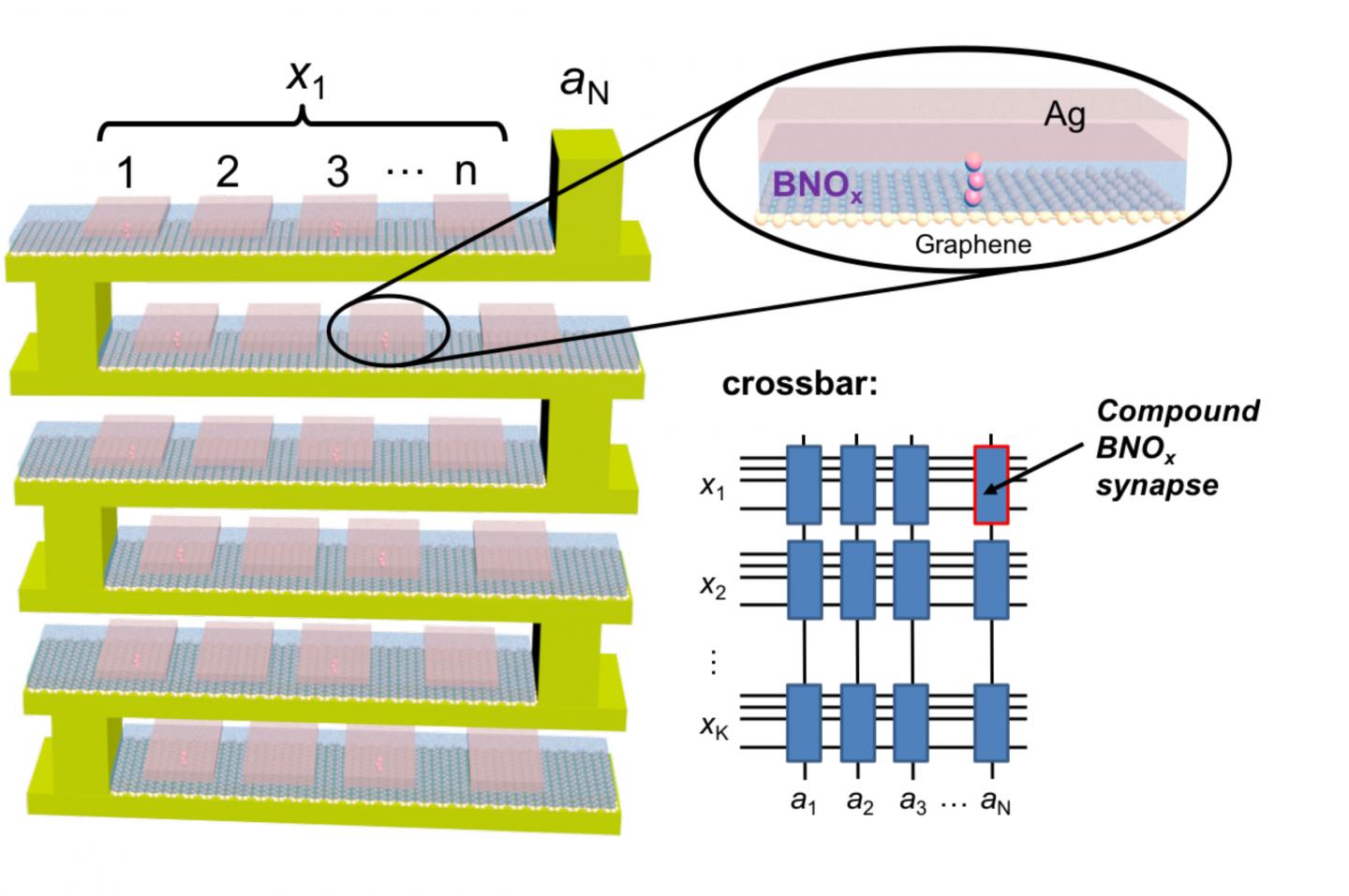
A group of researchers demonstrated a new type of compound synapse that can achieve synaptic weight programming and conduct vector-matrix multiplication with significant advances over the current state of the art. Publishing its work in the Journal of Applied Physics, from AIP Publishing, the group’s compound synapse is constructed with atomically thin boron nitride memristors running in parallel to ensure efficiency and accuracy.

The article appears in a special topic section of the journal devoted to “New Physics and Materials for Neuromorphic Computation,” which highlights new developments in physical and materials science research that hold promise for developing the very large-scale, integrated “neuromorphic” systems of tomorrow that will carry computation beyond the limitations of current semiconductors today.

“There’s a lot of interest in using new types of materials for memristors,” said Ivan Sanchez Esqueda, an author on the paper. “What we’re showing is that filamentary devices can work well for neuromorphic computing applications, when constructed in new clever ways.”

Current memristor technology suffers from a wide variation in how signals are stored and read across devices, both for different types of memristors as well as different runs of the same memristor. To overcome this, the researchers ran several memristors in parallel. The combined output can achieve accuracies up to five times those of conventional devices, an advantage that compounds as devices become more complex.

The choice to go to the subnanometer level, Sanchez said, was born out of an interest to keep all of these parallel memristors energy-efficient. An array of the group’s memristors were found to be 10,000 times more energy-efficient than memristors currently available.

“It turns out if you start to increase the number of devices in parallel, you can see large benefits in accuracy while still conserving power,” Sanchez said. Sanchez said the team next looks to further showcase the potential of the compound synapses by demonstrating their use completing increasingly complex tasks, such as image and pattern recognition.

Here’s an image illustrating the parallel artificial synapses,

Caption: Hardware that mimics the neural circuitry of the brain requires building blocks that can adjust how they synapse. One such approach, called memristors, uses current resistance to store this information. New work looks to overcome reliability issues in these devices by scaling memristors to the atomic level. Researchers demonstrated a new type of compound synapse that can achieve synaptic weight programming and conduct vector-matrix multiplication with significant advances over the current state of the art. They discuss their work in this week’s Journal of Applied Physics. This image shows a conceptual schematic of the 3D implementation of compound synapses constructed with boron nitride oxide (BNOx) binary memristors, and the crossbar array with compound BNOx synapses for neuromorphic computing applications. Credit: Ivan Sanchez Esqueda

Here’s a link to and a citation for the paper,

Efficient learning and crossbar operations with atomically-thin 2-D material compound synapses by Ivan Sanchez Esqueda, Huan Zhao and Han Wang. The article will appear in the Journal of Applied Physics Oct. 16, 2018 (DOI: 10.1063/1.5042468).

This paper is behind a paywall.

*Title corrected from ‘Two approaches to memristors featuring’ to ‘Two approaches to memristors’ on May 31, 2019 at 1455 hours PDT.

Hacking the human brain with a junction-based artificial synaptic device

Earlier today I published a piece featuring Dr. Wei Lu’s work on memristors and the movement to create an artificial brain (my June 28, 2017 posting: Dr. Wei Lu and bio-inspired ‘memristor’ chips). For this posting I’m featuring a non-memristor (if I’ve properly understood the technology) type of artificial synapse. From a June 28, 2017 news item on Nanowerk,

One of the greatest challenges facing artificial intelligence development is understanding the human brain and figuring out how to mimic it.

Now, one group reports in ACS Nano (“Emulating Bilingual Synaptic Response Using a Junction-Based Artificial Synaptic Device”) that they have developed an artificial synapse capable of simulating a fundamental function of our nervous system — the release of inhibitory and stimulatory signals from the same “pre-synaptic” terminal.

Unfortunately, the American Chemical Society news release on EurekAlert, which originated the news item, doesn’t provide too much more detail,

The human nervous system is made up of over 100 trillion synapses, structures that allow neurons to pass electrical and chemical signals to one another. In mammals, these synapses can initiate and inhibit biological messages. Many synapses just relay one type of signal, whereas others can convey both types simultaneously or can switch between the two. To develop artificial intelligence systems that better mimic human learning, cognition and image recognition, researchers are imitating synapses in the lab with electronic components. Most current artificial synapses, however, are only capable of delivering one type of signal. So, Han Wang, Jing Guo and colleagues sought to create an artificial synapse that can reconfigurably send stimulatory and inhibitory signals.

The researchers developed a synaptic device that can reconfigure itself based on voltages applied at the input terminal of the device. A junction made of black phosphorus and tin selenide enables switching between the excitatory and inhibitory signals. This new device is flexible and versatile, which is highly desirable in artificial neural networks. In addition, the artificial synapses may simplify the design and functions of nervous system simulations.

Here’s how I concluded that this is not a memristor-type device (from the paper [first paragraph, final sentence]; a link and citation will follow; Note: Links have been removed)),

The conventional memristor-type [emphasis mine](14-20) and transistor-type(21-25) artificial synapses can realize synaptic functions in a single semiconductor device but lacks the ability [emphasis mine] to dynamically reconfigure between excitatory and inhibitory responses without the addition of a modulating terminal.

Here’s a link to and a citation for the paper,

Emulating Bilingual Synaptic Response Using a Junction-Based Artificial Synaptic Device by
He Tian, Xi Cao, Yujun Xie, Xiaodong Yan, Andrew Kostelec, Don DiMarzio, Cheng Chang, Li-Dong Zhao, Wei Wu, Jesse Tice, Judy J. Cha, Jing Guo, and Han Wang. ACS Nano, Article ASAP DOI: 10.1021/acsnano.7b03033 Publication Date (Web): June 28, 2017

Copyright © 2017 American Chemical Society

This paper is behind a paywall.

Replace silicon with black phosphorus instead of graphene?

I have two black phosphorus pieces. This first piece of research comes out of ‘La belle province’ or, as it’s more usually called, Québec (Canada).

Foundational research on phosphorene

There’s a lot of interest in replacing silicon for a number of reasons and, increasingly, there’s interest in finding an alternative to graphene.

A July 7, 2015 news item on Nanotechnology Now describes a new material for use as transistors,

As scientists continue to hunt for a material that will make it possible to pack more transistors on a chip, new research from McGill University and Université de Montréal adds to evidence that black phosphorus could emerge as a strong candidate.

In a study published today in Nature Communications, the researchers report that when electrons move in a phosphorus transistor, they do so only in two dimensions. The finding suggests that black phosphorus could help engineers surmount one of the big challenges for future electronics: designing energy-efficient transistors.

A July 7, 2015 McGill University news release on EurekAlert, which originated the news item, describes the field of 2D materials and the research into black phosphorus and its 2D version, phosperene (analogous to graphite and graphene),

“Transistors work more efficiently when they are thin, with electrons moving in only two dimensions,” says Thomas Szkopek, an associate professor in McGill’s Department of Electrical and Computer Engineering and senior author of the new study. “Nothing gets thinner than a single layer of atoms.”

In 2004, physicists at the University of Manchester in the U.K. first isolated and explored the remarkable properties of graphene — a one-atom-thick layer of carbon. Since then scientists have rushed to to investigate a range of other two-dimensional materials. One of those is black phosphorus, a form of phosphorus that is similar to graphite and can be separated easily into single atomic layers, known as phosphorene.

Phosphorene has sparked growing interest because it overcomes many of the challenges of using graphene in electronics. Unlike graphene, which acts like a metal, black phosphorus is a natural semiconductor: it can be readily switched on and off.

“To lower the operating voltage of transistors, and thereby reduce the heat they generate, we have to get closer and closer to designing the transistor at the atomic level,” Szkopek says. “The toolbox of the future for transistor designers will require a variety of atomic-layered materials: an ideal semiconductor, an ideal metal, and an ideal dielectric. All three components must be optimized for a well designed transistor. Black phosphorus fills the semiconducting-material role.”

The work resulted from a multidisciplinary collaboration among Szkopek’s nanoelectronics research group, the nanoscience lab of McGill Physics Prof. Guillaume Gervais, and the nanostructures research group of Prof. Richard Martel in Université de Montréal’s Department of Chemistry.

To examine how the electrons move in a phosphorus transistor, the researchers observed them under the influence of a magnetic field in experiments performed at the National High Magnetic Field Laboratory in Tallahassee, FL, the largest and highest-powered magnet laboratory in the world. This research “provides important insights into the fundamental physics that dictate the behavior of black phosphorus,” says Tim Murphy, DC Field Facility Director at the Florida facility.

“What’s surprising in these results is that the electrons are able to be pulled into a sheet of charge which is two-dimensional, even though they occupy a volume that is several atomic layers in thickness,” Szkopek says. That finding is significant because it could potentially facilitate manufacturing the material — though at this point “no one knows how to manufacture this material on a large scale.”

“There is a great emerging interest around the world in black phosphorus,” Szkopek says. “We are still a long way from seeing atomic layer transistors in a commercial product, but we have now moved one step closer.”

Here’s a link to and a citation for the paper,

Two-dimensional magnetotransport in a black phosphorus naked quantum well by V. Tayari, N. Hemsworth, I. Fakih, A. Favron, E. Gaufrès, G. Gervais, R. Martel & T. Szkopek. Nature Communications 6, Article number: 7702 doi:10.1038/ncomms8702 Published 07 July 2015

This is an open access paper.

The second piece of research into black phosphorus is courtesy of an international collaboration.

A phosporene transistor

A July 9, 2015 Technical University of Munich (TUM) press release (also on EurekAlert) describes the formation of a phosphorene transistor made possible by the introduction of arsenic,

Chemists at the Technische Universität München (TUM) have now developed a semiconducting material in which individual phosphorus atoms are replaced by arsenic. In a collaborative international effort, American colleagues have built the first field-effect transistors from the new material.

For many decades silicon has formed the basis of modern electronics. To date silicon technology could provide ever tinier transistors for smaller and smaller devices. But the size of silicon transistors is reaching its physical limit. Also, consumers would like to have flexible devices, devices that can be incorporated into clothing and the likes. However, silicon is hard and brittle. All this has triggered a race for new materials that might one day replace silicon.

Black arsenic phosphorus might be such a material. Like graphene, which consists of a single layer of carbon atoms, it forms extremely thin layers. The array of possible applications ranges from transistors and sensors to mechanically flexible semiconductor devices. Unlike graphene, whose electronic properties are similar to those of metals, black arsenic phosphorus behaves like a semiconductor.

The press release goes on to provide more detail about the collaboration and the research,

A cooperation between the Technical University of Munich and the University of Regensburg on the German side and the University of Southern California (USC) and Yale University in the United States has now, for the first time, produced a field effect transistor made of black arsenic phosphorus. The compounds were synthesized by Marianne Koepf at the laboratory of the research group for Synthesis and Characterization of Innovative Materials at the TUM. The field effect transistors were built and characterized by a group headed by Professor Zhou and Dr. Liu at the Department of Electrical Engineering at USC.

The new technology developed at TUM allows the synthesis of black arsenic phosphorus without high pressure. This requires less energy and is cheaper. The gap between valence and conduction bands can be precisely controlled by adjusting the arsenic concentration. “This allows us to produce materials with previously unattainable electronic and optical properties in an energy window that was hitherto inaccessible,” says Professor Tom Nilges, head of the research group for Synthesis and Characterization of Innovative Materials.

Detectors for infrared

With an arsenic concentration of 83 percent the material exhibits an extremely small band gap of only 0.15 electron volts, making it predestined for sensors which can detect long wavelength infrared radiation. LiDAR (Light Detection and Ranging) sensors operate in this wavelength range, for example. They are used, among other things, as distance sensors in automobiles. Another application is the measurement of dust particles and trace gases in environmental monitoring.

A further interesting aspect of these new, two-dimensional semiconductors is their anisotropic electronic and optical behavior. The material exhibits different characteristics along the x- and y-axes in the same plane. To produce graphene like films the material can be peeled off in ultra thin layers. The thinnest films obtained so far are only two atomic layers thick.

Here’s a link to and a citation for the paper,

Black Arsenic–Phosphorus: Layered Anisotropic Infrared Semiconductors with Highly Tunable Compositions and Properties by Bilu Liu, Marianne Köpf, Ahmad N. Abbas, Xiaomu Wang, Qiushi Guo, Yichen Jia, Fengnian Xia, Richard Weihrich, Frederik Bachhuber, Florian Pielnhofer, Han Wang, Rohan Dhall, Stephen B. Cronin, Mingyuan Ge1 Xin Fang, Tom Nilges, and Chongwu Zhou. DOI: 10.1002/adma.201501758 Article first published online: 25 JUN 2015

© 2015 WILEY-VCH Verlag GmbH & Co. KGaA, Weinheim

This paper is behind a paywall.

Dexter Johnson, on his Nanoclast blog (on the Institute for Electrical and Electronics Engineers website), adds more information about black phosphorus and its electrical properties in his July 9, 2015 posting about the Germany/US collaboration (Note: Links have been removed),

Black phosphorus has been around for about 100 years, but recently it has been synthesized as a two-dimensional material—dubbed phosphorene in reference to its two-dimensional cousin, graphene. Black phosphorus is quite attractive for electronic applications like field-effect transistors because of its inherent band gap and it is one of the few 2-D materials to be a natively p-type semiconductor.

One final comment, I notice the Germany-US work was published weeks prior to the Canadian research suggesting that the TUM July 9, 2015 press release is an attempt to capitalize on the interest generated by the Canadian research. That’s a smart move.