Tag Archives: perovskites

The mystifying physics of paint-on semiconductors

I was not expecting a Canadian connection but it seems we are heavily invested in this research at the Georgia Institute of Technology (Georgia Tech), from a March 19, 2018 news item on ScienceDaily,

Some novel materials that sound too good to be true turn out to be true and good. An emergent class of semiconductors, which could affordably light up our future with nuanced colors emanating from lasers, lamps, and even window glass, could be the latest example.

These materials are very radiant, easy to process from solution, and energy-efficient. The nagging question of whether hybrid organic-inorganic perovskites (HOIPs) could really work just received a very affirmative answer in a new international study led by physical chemists at the Georgia Institute of Technology.

A March 19,. 2018 Georgia Tech news release (also on EurekAlert), which originated the news item, provides more detail,

The researchers observed in an HOIP a “richness” of semiconducting physics created by what could be described as electrons dancing on chemical underpinnings that wobble like a funhouse floor in an earthquake. That bucks conventional wisdom because established semiconductors rely upon rigidly stable chemical foundations, that is to say, quieter molecular frameworks, to produce the desired quantum properties.

“We don’t know yet how it works to have these stable quantum properties in this intense molecular motion,” said first author Felix Thouin, a graduate research assistant at Georgia Tech. “It defies physics models we have to try to explain it. It’s like we need some new physics.”

Quantum properties surprise

Their gyrating jumbles have made HOIPs challenging to examine, but the team of researchers from a total of five research institutes in four countries succeeded in measuring a prototypical HOIP and found its quantum properties on par with those of established, molecularly rigid semiconductors, many of which are graphene-based.

“The properties were at least as good as in those materials and may be even better,” said Carlos Silva, a professor in Georgia Tech’s School of Chemistry and Biochemistry. Not all semiconductors also absorb and emit light well, but HOIPs do, making them optoelectronic and thus potentially useful in lasers, LEDs, other lighting applications, and also in photovoltaics.

The lack of molecular-level rigidity in HOIPs also plays into them being more flexibly produced and applied.

Silva co-led the study with physicist Ajay Ram Srimath Kandada. Their team published the results of their study on two-dimensional HOIPs on March 8, 2018, in the journal Physical Review Materials. Their research was funded by EU Horizon 2020, the Natural Sciences and Engineering Research Council of Canada, the Fond Québécois pour la Recherche, the [National] Research Council of Canada, and the National Research Foundation of Singapore. [emphases mine]

The ‘solution solution’

Commonly, semiconducting properties arise from static crystalline lattices of neatly interconnected atoms. In silicon, for example, which is used in most commercial solar cells, they are interconnected silicon atoms. The same principle applies to graphene-like semiconductors.

“These lattices are structurally not very complex,” Silva said. “They’re only one atom thin, and they have strict two-dimensional properties, so they’re much more rigid.”

“You forcefully limit these systems to two dimensions,” said Srimath Kandada, who is a Marie Curie International Fellow at Georgia Tech and the Italian Institute of Technology. “The atoms are arranged in infinitely expansive, flat sheets, and then these very interesting and desirable optoelectronic properties emerge.”

These proven materials impress. So, why pursue HOIPs, except to explore their baffling physics? Because they may be more practical in important ways.

“One of the compelling advantages is that they’re all made using low-temperature processing from solutions,” Silva said. “It takes much less energy to make them.”

By contrast, graphene-based materials are produced at high temperatures in small amounts that can be tedious to work with. “With this stuff (HOIPs), you can make big batches in solution and coat a whole window with it if you want to,” Silva said.

Funhouse in an earthquake

For all an HOIP’s wobbling, it’s also a very ordered lattice with its own kind of rigidity, though less limiting than in the customary two-dimensional materials.

“It’s not just a single layer,” Srimath Kandada said. “There is a very specific perovskite-like geometry.” Perovskite refers to the shape of an HOIPs crystal lattice, which is a layered scaffolding.

“The lattice self-assembles,” Srimath Kandada said, “and it does so in a three-dimensional stack made of layers of two-dimensional sheets. But HOIPs still preserve those desirable 2D quantum properties.”

Those sheets are held together by interspersed layers of another molecular structure that is a bit like a sheet of rubber bands. That makes the scaffolding wiggle like a funhouse floor.

“At room temperature, the molecules wiggle all over the place. That disrupts the lattice, which is where the electrons live. It’s really intense,” Silva said. “But surprisingly, the quantum properties are still really stable.”

Having quantum properties work at room temperature without requiring ultra-cooling is important for practical use as a semiconductor.

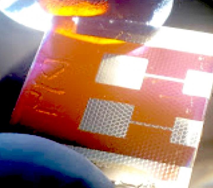
Going back to what HOIP stands for — hybrid organic-inorganic perovskites – this is how the experimental material fit into the HOIP chemical class: It was a hybrid of inorganic layers of a lead iodide (the rigid part) separated by organic layers (the rubber band-like parts) of phenylethylammonium (chemical formula (PEA)2PbI4).

The lead in this prototypical material could be swapped out for a metal safer for humans to handle before the development of an applicable material.

Electron choreography

HOIPs are great semiconductors because their electrons do an acrobatic square dance.

Usually, electrons live in an orbit around the nucleus of an atom or are shared by atoms in a chemical bond. But HOIP chemical lattices, like all semiconductors, are configured to share electrons more broadly.

Energy levels in a system can free the electrons to run around and participate in things like the flow of electricity and heat. The orbits, which are then empty, are called electron holes, and they want the electrons back.

“The hole is thought of as a positive charge, and of course, the electron has a negative charge,” Silva said. “So, hole and electron attract each other.”

The electrons and holes race around each other like dance partners pairing up to what physicists call an “exciton.” Excitons act and look a lot like particles themselves, though they’re not really particles.

Hopping biexciton light

In semiconductors, millions of excitons are correlated, or choreographed, with each other, which makes for desirable properties, when an energy source like electricity or laser light is applied. Additionally, excitons can pair up to form biexcitons, boosting the semiconductor’s energetic properties.

“In this material, we found that the biexciton binding energies were high,” Silva said. “That’s why we want to put this into lasers because the energy you input ends up to 80 or 90 percent as biexcitons.”

Biexcitons bump up energetically to absorb input energy. Then they contract energetically and pump out light. That would work not only in lasers but also in LEDs or other surfaces using the optoelectronic material.

“You can adjust the chemistry (of HOIPs) to control the width between biexciton states, and that controls the wavelength of the light given off,” Silva said. “And the adjustment can be very fine to give you any wavelength of light.”

That translates into any color of light the heart desires.

###

Coauthors of this paper were Stefanie Neutzner and Annamaria Petrozza from the Italian Institute of Technology (IIT); Daniele Cortecchia from IIT and Nanyang Technological University (NTU), Singapore; Cesare Soci from the Centre for Disruptive Photonic Technologies, Singapore; Teddy Salim and Yeng Ming Lam from NTU; and Vlad Dragomir and Richard Leonelli from the University of Montreal. …

Three Canadian science funding agencies plus European and Singaporean science funding agencies but not one from the US ? That’s a bit unusual for research undertaken at a US educational institution.

In any event, here’s a link to and a citation for the paper,

Stable biexcitons in two-dimensional metal-halide perovskites with strong dynamic lattice disorder by Félix Thouin, Stefanie Neutzner, Daniele Cortecchia, Vlad Alexandru Dragomir, Cesare Soci, Teddy Salim, Yeng Ming Lam, Richard Leonelli, Annamaria Petrozza, Ajay Ram Srimath Kandada, and Carlos Silva. Phys. Rev. Materials 2, 034001 – Published 8 March 2018

This paper is behind a paywall.

Beautiful solar cells based on insect eyes

What a gorgeous image!

The compound eye of a fly inspired Stanford researchers to create a compound solar cell consisting of perovskite microcells encapsulated in a hexagon-shaped scaffold. (Image credit: Thomas Shahan/Creative Commons)

An August 31, 2017 news item on Nanowerk describes research into solar cells being performed at Stanford University (Note: A link has been removed),

Packing tiny solar cells together, like micro-lenses in the compound eye of an insect, could pave the way to a new generation of advanced photovoltaics, say Stanford University scientists.

In a new study, the Stanford team used the insect-inspired design to protect a fragile photovoltaic material called perovskite from deteriorating when exposed to heat, moisture or mechanical stress. The results are published in the journal Energy & Environmental Science (“Scaffold-reinforced perovskite compound solar cells”).

An August 31, 2017 Stanford University news release (also on EurekAlert) by Mark Schwartz, which originated the news item,

“Perovskites are promising, low-cost materials that convert sunlight to electricity as efficiently as conventional solar cells made of silicon,” said Reinhold Dauskardt, a professor of materials science and engineering and senior author of the study. “The problem is that perovskites are extremely unstable and mechanically fragile. They would barely survive the manufacturing process, let alone be durable long term in the environment.”

Most solar devices, like rooftop panels, use a flat, or planar, design. But that approach doesn’t work well with perovskite solar cells.

“Perovskites are the most fragile materials ever tested in the history of our lab,” said graduate student Nicholas Rolston, a co-lead author of the E&ES study. “This fragility is related to the brittle, salt-like crystal structure of perovskite, which has mechanical properties similar to table salt.”

Eye of the fly

To address the durability challenge, the Stanford team turned to nature.

“We were inspired by the compound eye of the fly, which consists of hundreds of tiny segmented eyes,” Dauskardt explained. “It has a beautiful honeycomb shape with built-in redundancy: If you lose one segment, hundreds of others will operate. Each segment is very fragile, but it’s shielded by a scaffold wall around it.”

Scaffolds in a compound solar cell filled with perovskite after fracture testing.

Scaffolds in a compound solar cell filled with perovskite after fracture testing. (Image credit: Dauskardt Lab/Stanford University)

Using the compound eye as a model, the researchers created a compound solar cell consisting of a vast honeycomb of perovskite microcells, each encapsulated in a hexagon-shaped scaffold just 0.02 inches (500 microns) wide.

“The scaffold is made of an inexpensive epoxy resin widely used in the microelectronics industry,” Rolston said. “It’s resilient to mechanical stresses and thus far more resistant to fracture.”

Tests conducted during the study revealed that the scaffolding had little effect on how efficiently perovskite converted light into electricity.

“We got nearly the same power-conversion efficiencies out of each little perovskite cell that we would get from a planar solar cell,” Dauskardt said. “So we achieved a huge increase in fracture resistance with no penalty for efficiency.”

Durability

But could the new device withstand the kind of heat and humidity that conventional rooftop solar panels endure?

To find out, the researchers exposed encapsulated perovskite cells to temperatures of 185 F (85 C) and 85 percent relative humidity for six weeks. Despite these extreme conditions, the cells continued to generate electricity at relatively high rates of efficiency.

Dauskardt and his colleagues have filed a provisional patent for the new technology. To improve efficiency, they are studying new ways to scatter light from the scaffold into the perovskite core of each cell.

“We are very excited about these results,” he said. “It’s a new way of thinking about designing solar cells. These scaffold cells also look really cool, so there are some interesting aesthetic possibilities for real-world applications.”

Researchers have also made this image available,

Caption: A compound solar cell illuminated from a light source below. Hexagonal scaffolds are visible in the regions coated by a silver electrode. The new solar cell design could help scientists overcome a major roadblock to the development of perovskite photovoltaics. Credit: Dauskardt Lab/Stanford University

Not quite as weirdly beautiful as the insect eyes.

Here’s a link to and a citation for the paper,

Scaffold-reinforced perovskite compound solar cells by Brian L. Watson, Nicholas Rolston, Adam D. Printz, and Reinhold H. Dauskardt. Energy & Environmental Science 2017 DOI: 10.1039/C7EE02185B first published on 23 Aug 2017

This paper is behind a paywall.

Ferroelectric roadmap to neuromorphic computing

Having written about memristors and neuromorphic engineering a number of times here, I’m  quite intrigued to see some research into another nanoscale device for mimicking the functions of a human brain.

The announcement about the latest research from the team at the US Department of Energy’s Argonne National Laboratory is in a Feb. 14, 2017 news item on Nanowerk (Note: A link has been removed),

Research published in Nature Scientific Reports (“Ferroelectric symmetry-protected multibit memory cell”) lays out a theoretical map to use ferroelectric material to process information using multivalued logic – a leap beyond the simple ones and zeroes that make up our current computing systems that could let us process information much more efficiently.

A Feb. 10, 2017 Argonne National Laboratory news release by Louise Lerner, which originated the news item, expands on the theme,

The language of computers is written in just two symbols – ones and zeroes, meaning yes or no. But a world of richer possibilities awaits us if we could expand to three or more values, so that the same physical switch could encode much more information.

“Most importantly, this novel logic unit will enable information processing using not only “yes” and “no”, but also “either yes or no” or “maybe” operations,” said Valerii Vinokur, a materials scientist and Distinguished Fellow at the U.S. Department of Energy’s Argonne National Laboratory and the corresponding author on the paper, along with Laurent Baudry with the Lille University of Science and Technology and Igor Lukyanchuk with the University of Picardie Jules Verne.

This is the way our brains operate, and they’re something on the order of a million times more efficient than the best computers we’ve ever managed to build – while consuming orders of magnitude less energy.

“Our brains process so much more information, but if our synapses were built like our current computers are, the brain would not just boil but evaporate from the energy they use,” Vinokur said.

While the advantages of this type of computing, called multivalued logic, have long been known, the problem is that we haven’t discovered a material system that could implement it. Right now, transistors can only operate as “on” or “off,” so this new system would have to find a new way to consistently maintain more states – as well as be easy to read and write and, ideally, to work at room temperature.

Hence Vinokur and the team’s interest in ferroelectrics, a class of materials whose polarization can be controlled with electric fields. As ferroelectrics physically change shape when the polarization changes, they’re very useful in sensors and other devices, such as medical ultrasound machines. Scientists are very interested in tapping these properties for computer memory and other applications; but the theory behind their behavior is very much still emerging.

The new paper lays out a recipe by which we could tap the properties of very thin films of a particular class of ferroelectric material called perovskites.

According to the calculations, perovskite films could hold two, three, or even four polarization positions that are energetically stable – “so they could ‘click’ into place, and thus provide a stable platform for encoding information,” Vinokur said.

The team calculated these stable configurations and how to manipulate the polarization to move it between stable positions using electric fields, Vinokur said.

“When we realize this in a device, it will enormously increase the efficiency of memory units and processors,” Vinokur said. “This offers a significant step towards realization of so-called neuromorphic computing, which strives to model the human brain.”

Vinokur said the team is working with experimentalists to apply the principles to create a working system

Here’s a link to and a citation for the paper,

Ferroelectric symmetry-protected multibit memory cell by Laurent Baudry, Igor Lukyanchuk, & Valerii M. Vinokur. Scientific Reports 7, Article number: 42196 (2017) doi:10.1038/srep42196 Published online: 08 February 2017

This paper is open access.

Solar cells and soap bubbles

The MIT team has achieved the thinnest and lightest complete solar cells ever made, they say. To demonstrate just how thin and lightweight the cells are, the researchers draped a working cell on top of a soap bubble, without popping the bubble. Photo: Joel Jean and Anna Osherov

The MIT team has achieved the thinnest and lightest complete solar cells ever made, they say. To demonstrate just how thin and lightweight the cells are, the researchers draped a working cell on top of a soap bubble, without popping the bubble. Photo: Joel Jean and Anna Osherov

That’s quite a compelling image and it comes to us courtesy of researchers at MIT (Massachusetts Institute of Technology). From a Feb. 25, 2016 MIT news release (also on EurekAlert),

Imagine solar cells so thin, flexible, and lightweight that they could be placed on almost any material or surface, including your hat, shirt, or smartphone, or even on a sheet of paper or a helium balloon.

Researchers at MIT have now demonstrated just such a technology: the thinnest, lightest solar cells ever produced. Though it may take years to develop into a commercial product, the laboratory proof-of-concept shows a new approach to making solar cells that could help power the next generation of portable electronic devices.

Bulović [Vladimir Bulović ], MIT’s associate dean for innovation and the Fariborz Maseeh (1990) Professor of Emerging Technology, says the key to the new approach is to make the solar cell, the substrate that supports it, and a protective overcoating to shield it from the environment, all in one process. The substrate is made in place and never needs to be handled, cleaned, or removed from the vacuum during fabrication, thus minimizing exposure to dust or other contaminants that could degrade the cell’s performance.

“The innovative step is the realization that you can grow the substrate at the same time as you grow the device,” Bulović says.

In this initial proof-of-concept experiment, the team used a common flexible polymer called parylene as both the substrate and the overcoating, and an organic material called DBP as the primary light-absorbing layer. Parylene is a commercially available plastic coating used widely to protect implanted biomedical devices and printed circuit boards from environmental damage. The entire process takes place in a vacuum chamber at room temperature and without the use of any solvents, unlike conventional solar-cell manufacturing, which requires high temperatures and harsh chemicals. In this case, both the substrate and the solar cell are “grown” using established vapor deposition techniques.

One process, many materials

The team emphasizes that these particular choices of materials were just examples, and that it is the in-line substrate manufacturing process that is the key innovation. Different materials could be used for the substrate and encapsulation layers, and different types of thin-film solar cell materials, including quantum dots or perovskites, could be substituted for the organic layers used in initial tests.

But already, the team has achieved the thinnest and lightest complete solar cells ever made, they say. To demonstrate just how thin and lightweight the cells are, the researchers draped a working cell on top of a soap bubble, without popping the bubble. The researchers acknowledge that this cell may be too thin to be practical — “If you breathe too hard, you might blow it away,” says Jean [Joel Jean, doctoral student] — but parylene films of thicknesses of up to 80 microns can be deposited easily using commercial equipment, without losing the other benefits of in-line substrate formation.

A flexible parylene film, similar to kitchen cling-wrap but only one-tenth as thick, is first deposited on a sturdier carrier material – in this case, glass. Figuring out how to cleanly separate the thin material from the glass was a key challenge, explains Wang [Annie Wang, research scientist], who has spent many years working with parylene.

The researchers lift the entire parylene/solar cell/parylene stack off the carrier after the fabrication process is complete, using a frame made of flexible film. The final ultra-thin, flexible solar cells, including substrate and overcoating, are just one-fiftieth of the thickness of a human hair and one-thousandth of the thickness of equivalent cells on glass substrates — about two micrometers thick — yet they convert sunlight into electricity just as efficiently as their glass-based counterparts.

No miracles needed

“We put our carrier in a vacuum system, then we deposit everything else on top of it, and then peel the whole thing off,” explains Wang. Bulović says that like most new inventions, it all sounds very simple — once it’s been done. But actually developing the techniques to make the process work required years of effort.

While they used a glass carrier for their solar cells, Jean says “it could be something else. You could use almost any material,” since the processing takes place under such benign conditions. The substrate and solar cell could be deposited directly on fabric or paper, for example.

While the solar cell in this demonstration device is not especially efficient, because of its low weight, its power-to-weight ratio is among the highest ever achieved. That’s important for applications where weight is important, such as on spacecraft or on high-altitude helium balloons used for research. Whereas a typical silicon-based solar module, whose weight is dominated by a glass cover, may produce about 15 watts of power per kilogram of weight, the new cells have already demonstrated an output of 6 watts per gram — about 400 times higher.

“It could be so light that you don’t even know it’s there, on your shirt or on your notebook,” Bulović says. “These cells could simply be an add-on to existing structures.”

Still, this is early, laboratory-scale work, and developing it into a manufacturable product will take time, the team says. Yet while commercial success in the short term may be uncertain, this work could open up new applications for solar power in the long term. “We have a proof-of-concept that works,” Bulović says. The next question is, “How many miracles does it take to make it scalable? We think it’s a lot of hard work ahead, but likely no miracles needed.”

Here’s a link to and a citation for the paper,

In situ vapor-deposited parylene substrates for ultra-thin, lightweight organic solar cells by Joel Jean, Annie Wang, Vladimir Bulović. Organic Electronics Volume 31, April 2016, Pages 120–126 doi:10.1016/j.orgel.2016.01.022

This paper is behind a paywall.