Tag Archives: Nanyang Technological University (NTU)

Windows and roofs ‘self-adapt’ to heating and cooling conditions

I have two items about thermochromic coatings. It’s a little confusing since the American Association for the Advancement of Science (AAAS), which publishes the journal featuring both papers has issued a news release that seemingly refers to both papers as a single piece of research.

Onto, the press/new releases from the research institutions to be followed by the AAAS news release.

Nanyang Technological University (NTU) does windows

A December 16, 2021 news item on Nanowerk announced work on energy-saving glass,

An international research team led by scientists from Nanyang Technological University, Singapore (NTU Singapore) has developed a material that, when coated on a glass window panel, can effectively self-adapt to heat or cool rooms across different climate zones in the world, helping to cut energy usage.

Developed by NTU researchers and reported in the journal Science (“Scalable thermochromic smart windows with passive radiative cooling regulation”), the first-of-its-kind glass automatically responds to changing temperatures by switching between heating and cooling.

The self-adaptive glass is developed using layers of vanadium dioxide nanoparticles composite, Poly(methyl methacrylate) (PMMA), and low-emissivity coating to form a unique structure which could modulate heating and cooling simultaneously.

A December 17, 2021 NTU press release (PDF), also on EurekAlert but published December 16, 2021, which originated the news item, delves further into the research (Note: A link has been removed),

The newly developed glass, which has no electrical components, works by exploiting the spectrums of light responsible for heating and cooling.

During summer, the glass suppresses solar heating (near infrared light), while boosting radiative cooling (long-wave infrared) – a natural phenomenon where heat emits through surfaces towards the cold universe – to cool the room. In the winter, it does the opposite to warm up the room.

In lab tests using an infrared camera to visualise results, the glass allowed a controlled amount of heat to emit in various conditions (room temperature – above 70°C), proving its ability to react dynamically to changing weather conditions.

New glass regulates both heating and cooling

Windows are one of the key components in a building’s design, but they are also the least energy-efficient and most complicated part. In the United States alone, window-associated energy consumption (heating and cooling) in buildings accounts for approximately four per cent of their total primary energy usage each year according to an estimation based on data available from the Department of Energy in US.[1]

While scientists elsewhere have developed sustainable innovations to ease this energy demand – such as using low emissivity coatings to prevent heat transfer and electrochromic glass that regulate solar transmission from entering the room by becoming tinted – none of the solutions have been able to modulate both heating and cooling at the same time, until now.

The principal investigator of the study, Dr Long Yi of the NTU School of Materials Science and Engineering (MSE) said, “Most energy-saving windows today tackle the part of solar heat gain caused by visible and near infrared sunlight. However, researchers often overlook the radiative cooling in the long wavelength infrared. While innovations focusing on radiative cooling have been used on walls and roofs, this function becomes undesirable during winter. Our team has demonstrated for the first time a glass that can respond favourably to both wavelengths, meaning that it can continuously self-tune to react to a changing temperature across all seasons.”

As a result of these features, the NTU research team believes their innovation offers a convenient way to conserve energy in buildings since it does not rely on any moving components, electrical mechanisms, or blocking views, to function.

To improve the performance of windows, the simultaneous modulation of both solar transmission and radiative cooling are crucial, said co-authors Professor Gang Tan from The University of Wyoming, USA, and Professor Ronggui Yang from the Huazhong University of Science and Technology, Wuhan, China, who led the building energy saving simulation.

“This innovation fills the missing gap between traditional smart windows and radiative cooling by paving a new research direction to minimise energy consumption,” said Prof Gang Tan.

The study is an example of groundbreaking research that supports the NTU 2025 strategic plan, which seeks to address humanity’s grand challenges on sustainability, and accelerate the translation of research discoveries into innovations that mitigate human impact on the environment.

Innovation useful for a wide range of climate types

As a proof of concept, the scientists tested the energy-saving performance of their invention using simulations of climate data covering all populated parts of the globe (seven climate zones).

The team found the glass they developed showed energy savings in both warm and cool seasons, with an overall energy saving performance of up to 9.5%, or ~330,000 kWh per year (estimated energy required to power 60 household in Singapore for a year) less than commercially available low emissivity glass in a simulated medium sized office building.

First author of the study Wang Shancheng, who is Research Fellow and former PhD student of Dr Long Yi, said, “The results prove the viability of applying our glass in all types of climates as it is able to help cut energy use regardless of hot and cold seasonal temperature fluctuations. This sets our invention apart from current energy-saving windows which tend to find limited use in regions with less seasonal variations.”

Moreover, the heating and cooling performance of their glass can be customised to suit the needs of the market and region for which it is intended.

“We can do so by simply adjusting the structure and composition of special nanocomposite coating layered onto the glass panel, allowing our innovation to be potentially used across a wide range of heat regulating applications, and not limited to windows,” Dr Long Yi said.

Providing an independent view, Professor Liangbing Hu, Herbert Rabin Distinguished Professor, Director of the Center for Materials Innovation at the University of Maryland, USA, said, “Long and co-workers made the original development of smart windows that can regulate the near-infrared sunlight and the long-wave infrared heat. The use of this smart window could be highly important for building energy-saving and decarbonization.”  

A Singapore patent has been filed for the innovation. As the next steps, the research team is aiming to achieve even higher energy-saving performance by working on the design of their nanocomposite coating.

The international research team also includes scientists from Nanjing Tech University, China. The study is supported by the Singapore-HUJ Alliance for Research and Enterprise (SHARE), under the Campus for Research Excellence and Technological Enterprise (CREATE) programme, Minster of Education Research Fund Tier 1, and the Sino-Singapore International Joint Research Institute.

Here’s a link to and a citation for the paper,

Scalable thermochromic smart windows with passive radiative cooling regulation by Shancheng Wang, Tengyao Jiang, Yun Meng, Ronggui Yang, Gang Tan, and Yi Long. Science • 16 Dec 2021 • Vol 374, Issue 6574 • pp. 1501-1504 • DOI: 10.1126/science.abg0291

This paper is behind a paywall.

Lawrence Berkeley National Laboratory (Berkeley Lab; LBNL) does roofs

A December 16, 2021 Lawrence Berkeley National Laboratory news release (also on EurekAlert) announces an energy-saving coating for roofs (Note: Links have been removed),

Scientists have developed an all-season smart-roof coating that keeps homes warm during the winter and cool during the summer without consuming natural gas or electricity. Research findings reported in the journal Science point to a groundbreaking technology that outperforms commercial cool-roof systems in energy savings.

“Our all-season roof coating automatically switches from keeping you cool to warm, depending on outdoor air temperature. This is energy-free, emission-free air conditioning and heating, all in one device,” said Junqiao Wu, a faculty scientist in Berkeley Lab’s Materials Sciences Division and a UC Berkeley professor of materials science and engineering who led the study.

Today’s cool roof systems, such as reflective coatings, membranes, shingles, or tiles, have light-colored or darker “cool-colored” surfaces that cool homes by reflecting sunlight. These systems also emit some of the absorbed solar heat as thermal-infrared radiation; in this natural process known as radiative cooling, thermal-infrared light is radiated away from the surface.

The problem with many cool-roof systems currently on the market is that they continue to radiate heat in the winter, which drives up heating costs, Wu explained.

“Our new material – called a temperature-adaptive radiative coating or TARC – can enable energy savings by automatically turning off the radiative cooling in the winter, overcoming the problem of overcooling,” he said.

A roof for all seasons

Metals are typically good conductors of electricity and heat. In 2017, Wu and his research team discovered that electrons in vanadium dioxide behave like a metal to electricity but an insulator to heat – in other words, they conduct electricity well without conducting much heat. “This behavior contrasts with most other metals where electrons conduct heat and electricity proportionally,” Wu explained.

Vanadium dioxide below about 67 degrees Celsius (153 degrees Fahrenheit) is also transparent to (and hence not absorptive of) thermal-infrared light. But once vanadium dioxide reaches 67 degrees Celsius, it switches to a metal state, becoming absorptive of thermal-infrared light. This ability to switch from one phase to another – in this case, from an insulator to a metal – is characteristic of what’s known as a phase-change material.

To see how vanadium dioxide would perform in a roof system, Wu and his team engineered a 2-centimeter-by-2-centimeter TARC thin-film device.

TARC “looks like Scotch tape, and can be affixed to a solid surface like a rooftop,” Wu said.

In a key experiment, co-lead author Kechao Tang set up a rooftop experiment at Wu’s East Bay home last summer to demonstrate the technology’s viability in a real-world environment.

A wireless measurement device set up on Wu’s balcony continuously recorded responses to changes in direct sunlight and outdoor temperature from a TARC sample, a commercial dark roof sample, and a commercial white roof sample over multiple days.

How TARC outperforms in energy savings

The researchers then used data from the experiment to simulate how TARC would perform year-round in cities representing 15 different climate zones across the continental U.S.

Wu enlisted Ronnen Levinson, a co-author on the study who is a staff scientist and leader of the Heat Island Group in Berkeley Lab’s Energy Technologies Area, to help them refine their model of roof surface temperature. Levinson developed a method to estimate TARC energy savings from a set of more than 100,000 building energy simulations that the Heat Island Group previously performed to evaluate the benefits of cool roofs and cool walls across the United States.

Finnegan Reichertz, a 12th grade student at the East Bay Innovation Academy in Oakland who worked remotely as a summer intern for Wu last year, helped to simulate how TARC and the other roof materials would perform at specific times and on specific days throughout the year for each of the 15 cities or climate zones the researchers studied for the paper.

The researchers found that TARC outperforms existing roof coatings for energy saving in 12 of the 15 climate zones, particularly in regions with wide temperature variations between day and night, such as the San Francisco Bay Area, or between winter and summer, such as New York City.

“With TARC installed, the average household in the U.S. could save up to 10% electricity,” said Tang, who was a postdoctoral researcher in the Wu lab at the time of the study. He is now an assistant professor at Peking University in Beijing, China.

Standard cool roofs have high solar reflectance and high thermal emittance (the ability to release heat by emitting thermal-infrared radiation) even in cool weather.

According to the researchers’ measurements, TARC reflects around 75% of sunlight year-round, but its thermal emittance is high (about 90%) when the ambient temperature is warm (above 25 degrees Celsius or 77 degrees Fahrenheit), promoting heat loss to the sky. In cooler weather, TARC’s thermal emittance automatically switches to low, helping to retain heat from solar absorption and indoor heating, Levinson said.

Findings from infrared spectroscopy experiments using advanced tools at Berkeley Lab’s Molecular Foundry validated the simulations.

“Simple physics predicted TARC would work, but we were surprised it would work so well,” said Wu. “We originally thought the switch from warming to cooling wouldn’t be so dramatic. Our simulations, outdoor experiments, and lab experiments proved otherwise – it’s really exciting.”

The researchers plan to develop TARC prototypes on a larger scale to further test its performance as a practical roof coating. Wu said that TARC may also have potential as a thermally protective coating to prolong battery life in smartphones and laptops, and shield satellites and cars from extremely high or low temperatures. It could also be used to make temperature-regulating fabric for tents, greenhouse coverings, and even hats and jackets.

Co-lead authors on the study were Kaichen Dong and Jiachen Li.

The Molecular Foundry is a nanoscience user facility at Berkeley Lab.

This work was primarily supported by the DOE Office of Science and a Bakar Fellowship.

The technology is available for licensing and collaboration. If interested, please contact Berkeley Lab’s Intellectual Property Office, ipo@lbl.gov.

Here’s a link to and a citation for the paper,

Temperature-adaptive radiative coating for all-season household thermal regulation by Kechao Tang, Kaichen Dong, Jiachen Li, Madeleine P. Gordon, Finnegan G. Reichertz, Hyungjin Kim, Yoonsoo Rho, Qingjun Wang, Chang-Yu Lin, Costas P. Grigoropoulos, Ali Javey, Jeffrey J. Urban, Jie Yao, Ronnen Levinson, Junqiao Wu. Science • 16 Dec 2021 • Vol 374, Issue 6574 • pp. 1504-1509 • DOI: 10.1126/science.abf7136

This paper is behind a paywall.

An interesting news release from the AAAS

While it’s a little confusing as it cites only the ‘window’ research from NTU, the body of this news release offers some additional information about the usefulness of thermochromic materials and seemingly refers to both papers, from a December 16, 2021 AAAS news release,

Temperature-adaptive passive radiative cooling for roofs and windows

When it’s cold out, window glass and roof coatings that use passive radiative cooling to keep buildings cool can be designed to passively turn off radiative cooling to avoid heat loss, two new studies show.  Their proof-of-concept analyses demonstrate that passive radiative cooling can be expanded to warm and cold climate applications and regions, potentially providing all-season energy savings worldwide. Buildings consume roughly 40% of global energy, a large proportion of which is used to keep them cool in warmer climates. However, most temperature regulation systems commonly employed are not very energy efficient and require external power or resources. In contrast, passive radiative cooling technologies, which use outer space as a near-limitless natural heat sink, have been extensively examined as a means of energy-efficient cooling for buildings. This technology uses materials designed to selectively emit narrow-band radiation through the infrared atmospheric window to disperse heat energy into the coldness of space. However, while this approach has proven effective in cooling buildings to below ambient temperatures, it is only helpful during the warmer months or in regions that are perpetually hot. Furthermore, the inability to “turn off” passive cooling in cooler climes or in regions with large seasonal temperature variations means that continuous cooling during colder periods would exacerbate the energy costs of heating. In two different studies, by Shancheng Wang and colleagues and Kechao Tang and colleagues, researchers approach passive radiative cooling from an all-season perspective and present a new, scalable temperature-adaptive radiative technology that passively turns off radiative cooling at lower temperatures. Wang et al. and Tang et al. achieve this using a tungsten-doped vanadium dioxide and show how it can be applied to create both window glass and a flexible roof coating, respectively. Model simulations of the self-adapting materials suggest they could provide year-round energy savings across most climate zones, especially those with substantial seasonal temperature variations. 

I wish them all good luck with getting these materials to market.
Cellulose nanocrystals (CNC), protein, and starch eletrospun to develop ‘smart’ food packaging

A December 29, 2021 news item on ScienceDaily announces research into ;smart’ sustainable packaging from a joint Nanyang Technical University and Harvard University,

A team of scientists from Nanyang Technological University, Singapore (NTU Singapore) and Harvard T.H. Chan School of Public Health, US, has developed a ‘smart’ food packaging material that is biodegradable, sustainable and kills microbes that are harmful to humans. It could also extend the shelf-life of fresh fruit by two to three days.

The waterproof food packaging is made from a type of corn protein called zein, starch and other naturally derived biopolymers, infused with a cocktail of natural antimicrobial compounds. These include oil from thyme, a common herb used in cooking, and citric acid, which is commonly found in citrus fruits.

A December 28, 2021 Nanyang Technological University press release (PDF), also on EurekAlert but published December 27, 2021, which originated the news item, offers a few more details about the research (Note 1: Links have been removed; Note 2: I had to dig into the abstract to find the cellulose nanocrystals),

In lab experiments, when exposed to an increase in humidity or enzymes from harmful bacteria, the fibres in the packaging have been shown to release the natural antimicrobial compounds, killing common dangerous bacteria that contaminate food, such as E. Coli and Listeria, as well as fungi.

The packaging is designed to release the necessary miniscule amounts of antimicrobial compounds only in response to the presence of additional humidity or bacteria. This ensures that the packaging can endure several exposures, and last for months.

As the compounds combat any bacteria that grow on the surface of the packaging as well as on the food product itself, it has the potential to be used for a large variety of products, including ready-to-eat foods, raw meat, fruits, and vegetables.

In an experiment, strawberries that were wrapped in the packaging stayed fresh for seven days before developing mould, compared to counterparts that were kept in mainstream fruit plastic boxes, which only stayed fresh for four days.

The invention is the result of the collaboration by scientists from the NTU-Harvard T. H. Chan School of Public Health Initiative for Sustainable Nanotechnology (NTU-Harvard SusNano), which brings together NTU and Harvard Chan School researchers to work on cutting edge applications in agriculture and food, with an emphasis on developing non-toxic and environmentally safe nanomaterials.

The development of this advanced food packaging material is part of the University’s efforts to promote sustainable food tech solutions, that is aligned with the NTU 2025 strategic plan, which aims to develop sustainable solutions to address some of humanity’s pressing grand challenges.

Professor Mary Chan, Director of NTU’s Centre of Antimicrobial Bioengineering, who co-led the project, said: “This invention would serve as a better option for packaging in the food industry, as it has demonstrated superior antimicrobial qualities in combatting a myriad of food-related bacteria and fungi that could be harmful to humans. The packaging can be applied to various produces such as fish, meat, vegetables, and fruits. The smart release of antimicrobials only when bacteria or high humidity is present, provides protection only when needed thus minimising the use of chemicals and preserving the natural composition of foods packaged.”

Professor Philip Demokritou, Adjunct Professor of Environmental Health at Harvard Chan School, who is also Director of Nanotechnology and Nanotoxicology Center and Co-director of NTU-Harvard Initiative on Sustainable Nanotechnology, who co-led the study, said: “Food safety and waste have become a major societal challenge of our times with immense public health and economic impact which compromises food security. One of the most efficient ways to enhance food safety and reduce spoilage and waste is to develop efficient biodegradable non-toxic food packaging materials. In this study, we used nature-derived compounds including biopolymers, non-toxic solvents, and nature-inspired antimicrobials and develop scalable systems to synthesise smart antimicrobial materials which can be used not only to enhance food safety and quality but also to eliminate the harm to the environment and health and reduce the use of non-biodegradable plastics at global level and promote sustainable agri-food systems.” 

Providing an independent assessment of the work done by the NTU research team, Mr Peter Barber, CEO of ComCrop, a Singapore company that pioneered urban rooftop farming, said: “The NTU-Harvard Chan School food packaging material would serve as a sustainable solution for companies like us who want to cut down on the usage of plastic and embrace greener alternatives. As ComCrop looks to ramp up product to boost Singapore’s food production capabilities, the volume of packaging we need will increase in sync, and switching to a material such as this would help us have double the impact. The wrapping’s antimicrobial properties, which could potentially extend the shelf life of our vegetables, would serve us well. The packaging material holds promise to the industry, and we look forward to learning more about the wrapping and possibly adopting it for our usage someday.”

The results of the study were published in the peer-reviewed academic journal ACS Applied Materials & Interfacesin October [2021].

Cutting down on packaging waste

The packaging industry is the largest and growing consumer of synthetic plastics derived from fossil fuels, with food packaging plastics accounting for the bulk of plastic waste that are polluting the environment.

In Singapore, packaging is a major source of trash, with data from Singapore’s National Environment Agency showing that out of the 1.76 million tonnes of waste disposed of by domestic sources in 2018, one third of it was packaging waste, and over half of it (55 per cent) was plastic.

The smart food package material, when scaled up, could serve as an alternative to cut down on the amount of plastic waste, as it is biodegradable. Its main ingredient, zein, is also produced from corn gluten meal, which is a waste by-product from using corn starch or oils in order to produce ethanol.

The food packaging material is produced by electrospinning[1] the zein, the antimicrobial compounds with cellulose, a natural polymer starch that makes up plant cell walls, and acetic acid, which is commonly found in vinegar.

Prof Mary Chan added: “The sustainable and biodegradable active food packaging, which has inbuilt technology to keep bacteria and fungus at bay, is of great importance to the food industry. It could serve as an environmentally friendly alternative to petroleum-based polymers used in commercial food packaging, such as plastic, which have a significant negative environmental impact.”

Prof Demokritou added: “Due to the globalisation of food supply and attitude shift towards a healthier lifestyle and environmentally friendly food packaging, there is a need to develop biodegradable, non-toxic and smart/responsive materials to enhance food safety and quality. Development of scalable synthesis platforms for developing food packaging materials that are composed of nature derived, biodegradable biopolymers and nature inspired antimicrobials, coupled with stimuli triggered approaches will meet the emerging societal needs to reduce food waste and enhance food safety and quality.”

The team of NTU and Harvard Chan School researchers hope to scale up their technology with an industrial partner, with the aim of commercialisation within the next few years.

They are also currently working on developing other technologies to develop biopolymer-based smart food package materials to enhance food safety and quality.

Here’s a link to and a citation for the paper, followed by the key (nanocellulose crystal mention) sentences in the abstract,

Enzyme- and Relative Humidity-Responsive Antimicrobial Fibers for Active Food Packaging by Zeynep Aytac, Jie Xu, Suresh Kumar Raman Pillai, Brian D. Eitzer, Tao Xu, Nachiket Vaze, Kee Woei Ng, Jason C. White, Mary B. Chan-Park, Yaguang Luo, and Philip Demokritou. ACS Appl. Mater. Interfaces 2021, 13, 42, 50298–50308 I: https://doi.org/10.1021/acsami.1c12319 Publication Date: October 14, 2021 Copyright © 2021 American Chemical Society

This paper is behind a paywall.

Excerpt from abstract,

Active food packaging materials that are sustainable, biodegradable, and capable of precise delivery of antimicrobial active ingredients (AIs) are in high demand. Here, we report the development of novel enzyme- and relative humidity (RH)-responsive antimicrobial fibers with an average diameter of 225 ± 50 nm, which can be deposited as a functional layer for packaging materials. Cellulose nanocrystals (CNCs) [emphasis mine], zein (protein), and starch were electrospun to form multistimuli-responsive fibers that incorporated a cocktail of both free nature-derived antimicrobials such as thyme oil, citric acid, and nisin and cyclodextrin-inclusion complexes (CD-ICs) of thyme oil, sorbic acid, and nisin. …

I have been following the CNC story for some time. If you’re curious, just use ‘cellulose nanocrystal(s)’ as your search term. You can find out more about ComCrop here.

Singapore contributes to art/science gallery on the International Space Station (ISS)

A March 15, 2022 Nanyang Technological University press release (also on EurekAlert) announces Singapore’s contribution to an art gallery in space,

Two Singapore-designed artefacts are now orbiting around the Earth on the International Space Station (ISS), as part of Moon Gallery.

These artworks were successfully launched into space recently as part of a test flight by the Moon Gallery and will come back to Earth after 10 months.

Currently consisting of 64 artworks made by artists all around the world, the Moon gallery will eventually consist of 100 artworks, which will then be placed on the moon by 2025. Out of these 64 art pieces on the ISS, only two are Singaporean artworks.

Here’s Singapore’s contribution,

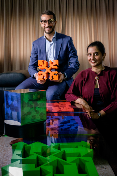
Caption: NTU [Nanyang Technological University] Singapore Assistant Professor Matteo Seita (left), who is holding the Cube of Interaction, and Ms Lakshmi Mohanbabu (right), who designed both cubes. The Structure & Reflectance cube in the foreground was 3D printed at NTU Singapore.. Credit: NTU Singapore

A December 8, 2021 news item on phys.org describes the project,

The Moon Gallery Foundation is developing an art gallery to be sent to the Moon, contributing to the establishment of the first lunar outpost and permanent museum on Earth’s only natural satellite. The international initiative will see one hundred artworks from artists around the world integrated into a 10 cm x 10 cm x 1 cm grid tray, which will fly to the Moon by 2025. The Moon Gallery aims to expand humanity’s cultural dialog beyond Earth. The gallery will meet the cosmos for the first time in low Earth orbit in 2022 in a test flight.

The test flight is in collaboration with Nanoracks, a private in-space service provider. The gallery is set to fly to the International Space Station (ISS) aboard the NG-17 rocket as part of a Northrop Grumman Cygnus resupply mission in February of 2022. The art projects featured in the gallery will reach the final frontier of human habitat in space, and mark the historical meeting point of the Moon Gallery and the cosmos. Reaching low Earth orbit on the way to the Moon is a pivotal first step in extending our cultural dialog to space.

On its return flight, the Moon Gallery will become a part of the NanoLab technical payload, a module for space research experiments. The character of the gallery will offer a diverse range of materials and behaviors for camera observations and performance tests with NanoLab.

In return, Moon Gallery artists will get a chance to learn about the performance of their artworks in space. The result of these observations will serve as a solid basis for the subsequent Moon Gallery missions and a source of a valuable learning experience for future space artists. The test flight to the ISS is a precursor mission, contributing to the understanding of future possibilities for art in space and strengthening collaboration between the art and space sectors.

A December 8, 2021 NYU press release on EurekAlert, which originated the news item, provides more detail about the art from Singapore,

STRUCTURE & REFLECTANCE CUBE

Our every perception, analysis, and thought reflect the influences from our surroundings and the Universe in a world of collaboration, communication and interaction, making it possible to explore the real, the imagined and the unknown. The ‘Structure and Reflectance’ cube, a marriage of Art and Technology, is one of the hundred artworks selected by the Moon Gallery, with a unifying message of an integrated world, making it a quintessential signature of humankind on the Moon.

Ms Lakshmi Mohanbabu, a Singaporean architect and designer, is the first and only local artist to have her artwork selected for the Moon Gallery. Coined the ‘Structure and Reflectance’ cube, Lakshmi’s art is a marriage of Art and Technology and is one of the hundred artworks selected by the Moon Gallery. The cube signifies a unifying message of an integrated world, making it a quintessential signature of humankind on the Moon.

The early-stage prototyping and design iterations of the ‘Structure and Reflectance’ cube were performed with Additive Manufacturing, otherwise known as 3D printing, at Nanyang Technological University, Singapore’s (NTU Singapore)Singapore Centre for 3D Printing (SC3DP). This was part of a collaborative project supported by the National Additive Manufacturing Innovation Cluster (NAMIC), a national programme office which accelerates the adoption and commercialisation of additive manufacturing technologies. Previously, the NTU Singapore team at SC3DP produced a few iterations of Moon-Cube using metal 3D printing in various materials such as Inconel and Stainless Steel to evaluate the best suited material.

The newest iteration of the cube comprises crystals—ingrained in the cube via additive manufacturing technology— revealed to the naked eye by the microscopic differences in their surface roughness, which reflect light along different directions.

“Additive Manufacturing is suitable for enabling this level of control over the crystal structure of solids. More specifically, the work was created using ‘laser powder bed fusion technology’ a metal additive manufacturing process which allows us to control the surface roughness through varying the laser parameter,” said Dr Matteo Seita, Nanyang Assistant Professor, NTU Singapore, is the Principal Investigator overseeing the project for the current cube design.  

Dr Seita shared the meaning behind the materials used, “Like people, materials have a complex ‘structure’ resulting from their history—the sequence of processes that have shaped their constituent parts—which underpins their differences. Masked by an exterior façade, this structure often reveals little of the underlying quality in materials or people. The cube is a material representation of a human’s complex structure embodied in a block of metal consisting of two crystals with distinct reflectivity and complementary shape.”

Ms Lakshmi added, “The optical contrast on the cube surface from the crystals generates an intricate geometry which signifies the duality of man: the complexity of hidden thought and expressed emotion. This duality is reflected by the surface of the Moon where one side remains in plain sight, while the other has remained hidden to humankind for centuries; until space travel finally allowed humanity to gaze upon it. The bright portion of the visible side of the Moon is dependent on the Moon’s position relative to the Earth and the Sun. Thus, what we see is a function of our viewpoint.”

The hidden structure of materials, people, and the Moon are visualized as reflections of light through art and science in this cube. Expressed in the Structure & Reflectance cube is the concept of human’s duality—represented by two crystals with different reflectance—which appears to the observer as a function of their perspective.

Dr Ho Chaw Sing, Co-Founder and Managing Director of NAMIC said, “Space is humanity’s next frontier. Being the only Singaporean – among a selected few from the global community – Lakshmi’s 3D printed cube presents a unique perspective through the fusion of art and technology. We are proud to have played a small role supporting her in this ‘moon-shot’ initiative.”

Lakshmi views each artwork as a portrayal of humanity’s quests to discover the secrets of the Universe and—fused into a single cube—embody the unity of humankind, which transcends our differences in culture, religion, and social status.

The first cube face, the Primary, is divided into two triangles and depicts the two faces of the Moon, one visible to us from the earth and the other hidden from our view.

The second cube face, the Windmill, has two spiralling windmill forms, one clockwise and the other counter-clockwise, representing our existence, energy, and time.

The third cube face, the Dromenon, is a labyrinth form of nested squares, which represents the layers that we—as space explorers—are unravelling to discover the enigma of the Universe. 

The fourth cube face, the Nautilus, reflects the spiralling form of our DNA that makes each of us unique, a shape reflected in the form of our galaxy.

Not having heard of the Moon Gallery or the Moon Gallery Foundation, I did a little research. There’s a LinkedIn profile for the Moon Gallery Foundation (both the foundation and the gallery are located in Holland [Netherlands]),

Moon Gallery is where art and space meet. We aim to set up the first permanent museum on the Moon and develop a culture for future interplanetary society.

Moon Gallery will launch 100 artefacts to the Moon within the compact format of 10 x 10 x 1cm plate on a lunar lander exterior panelling no later than 2025. We suggest bringing this collection of ideas as the seeds of a new culture. We believe that culture makes a distinction between mere survival and life. Moon Gallery is a symbolic gesture that has a real influence – a way to reboot culture, rethink our values for better living on Earth planet.

The Moon Gallery has its own website, where I found more information about events, artists, and partners such as Nanoracks,

Nanoracks is dedicated to using our unique expertise to solve key problems both in space and on the Earth – all while lowering the barriers to entry of space exploration. Nanoracks’s main office is in Houston, Texas. The business development office is in Washington, D.C., and additional offices are located in Abu Dhabi, United Arab Emirates (UAE) and Turin, Italy. Nanoracks provides tools, hardware and services that allow other companies, organizations and governments to conduct research and other projects in space. Some of Nanoracks customers include Student Spaceflight Experiments Program (SSEP), the European Space Agency (ESA), the German Space Agency (DLR), NASA, Planet Labs, Space Florida, Virgin Galactic, Adidas, Aerospace Corporation, National Reconnaissance Office (NRO), UAE Space Agency, Mohammed bin Rashid Space Centre (MBRSC), and the Beijing Institute of Technology.

You can find the Nanoracks website here.

Living plants detect arsenic by way of embedded nanosensors

There’s a lot of arsenic in the world and it’s often a factor in making water undrinkable. When that water is used in farming It also pollutes soil and enters food-producing plants. A December 11, 2020 news item on Nanowerk announces research into arsenic detectors in plants,

Researchers have developed a living plant-based sensor that can in real-time detect and monitor levels of arsenic, a highly toxic heavy metal, in the soil. Arsenic pollution is a major threat to humans and ecosystems in many Asia Pacific countries.

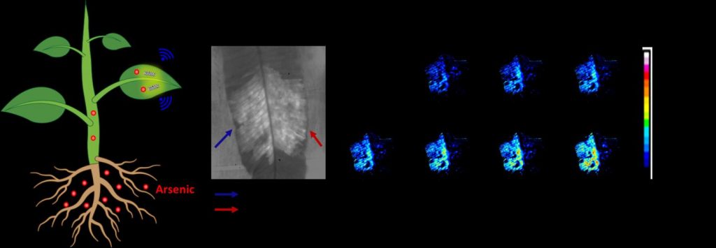
Caption: Non-destructive plant nanobionic sensor embedded within leaves to report arsenic levels within plants to portable electronics, enabling real-time monitoring of arsenic uptake in living plants. Credit: Dr. Tedrick Thomas Salim Lew

I was not able to find the source for the news item but I did locate something close. From a December 13, 2020 Singapore-Massachusetts Institute of Technology (MIT) Alliance for Research and Technology (SMART), also on EurekAlert,

Scientists from the Disruptive and Sustainable Technologies for Agricultural Precision (DiSTAP) research group at the Singapore-MIT Alliance for Research and Technology (SMART), MIT’s research enterprise in Singapore, have engineered a novel type of plant nanobionic optical sensor that can detect and monitor, in real time, levels of the highly toxic heavy metal arsenic in the underground environment. This development provides significant advantages over conventional methods used to measure arsenic in the environment and will be important for both environmental monitoring and agricultural applications to safeguard food safety, as arsenic is a contaminant in many common agricultural products such as rice, vegetables, and tea leaves.

Arsenic and its compounds are a serious threat to humans and ecosystems. Long-term exposure to arsenic in humans can cause a wide range of detrimental health effects, including cardiovascular disease such as heart attack, diabetes, birth defects, severe skin lesions, and numerous cancers including those of the skin, bladder, and lung. Elevated levels of soil arsenic as a result of anthropogenic activities such as mining and smelting are also harmful to plants, inhibiting growth and resulting in substantial crop losses.

Food crops can absorb arsenic from the soil, leading to contamination of food and produce consumed by humans. Arsenic in underground environments can also contaminate groundwater and other underground water sources, the long-term consumption of which can cause severe health issues. As such, developing accurate, effective, and easy-to-deploy arsenic sensors is important to protect both the agriculture industry and wider environmental safety.

The novel optical nanosensors exhibit changes in their fluorescence intensity upon detecting arsenic. Embedded in plant tissues, with no detrimental effects on the plant, these sensors provide a nondestructive way to monitor the internal dynamics of arsenic taken up by plants from the soil. This integration of optical nanosensors within living plants enables the conversion of plants into self-powered detectors of arsenic from their natural environment, marking a significant upgrade from the time- and equipment-intensive arsenic sampling methods of current conventional methods.

“Our plant-based nanosensor is notable not only for being the first of its kind, but also for the significant advantages it confers over conventional methods of measuring arsenic levels in the below-ground environment, requiring less time, equipment, and manpower,” says Lew. “We envision that this innovation will eventually see wide use in the agriculture industry and beyond. I am grateful to SMART DiSTAP and the Temasek Life Sciences Laboratory (TLL), both of which were instrumental in idea generation and scientific discussion as well as research funding for this work.”

Besides detecting arsenic in rice and spinach, the team also used a species of fern, Pteris cretica, which can hyperaccumulate arsenic. This fern species can absorb and tolerate high levels of arsenic with no detrimental effect — engineering an ultrasensitive plant-based arsenic detector, capable of detecting very low concentrations of arsenic, as low as 0.2 parts per billion. In contrast, the regulatory limit for arsenic detectors is 10 parts per billion. Notably, the novel nanosensors can also be integrated into other species of plants. The researchers say this is the first successful demonstration of living plant-based sensors for arsenic and represents a groundbreaking advancement that could prove highly useful in both agricultural research (e.g., to monitor arsenic taken up by edible crops for food safety) and general environmental monitoring.

Previously, conventional methods of measuring arsenic levels included regular field sampling, plant tissue digestion, extraction, and analysis using mass spectrometry. These methods are time-consuming, require extensive sample treatment, and often involve the use of bulky and expensive instrumentation. The new approach couples nanoparticle sensors with plants’ natural ability to efficiently extract analytes via the roots and transport them. This allows for the detection of arsenic uptake in living plants in real time, with portable, inexpensive electronics such as a portable Raspberry Pi platform equipped with a charge-coupled device camera akin to a smartphone camera.

Co-author, DiSTAP co-lead principal investigator, and MIT Professor Michael Strano adds, “This is a hugely exciting development, as, for the first time, we have developed a nanobionic sensor that can detect arsenic — a serious environmental contaminant and potential public health threat. With its myriad advantages over older methods of arsenic detection, this novel sensor could be a game-changer, as it is not only more time-efficient, but also more accurate and easier to deploy than older methods. It will also help plant scientists in organizations such as TLL to further produce crops that resist uptake of toxic elements. Inspired by TLL’s recent efforts to create rice crops which take up less arsenic, this work is a parallel effort to further support SMART DiSTAP’s efforts in food security research, constantly innovating and developing new technological capabilities to improve Singapore’s food quality and safety.”

The research is carried out by SMART and supported by the National Research Foundation (NRF) Singapore under its Campus for Research Excellence And Technological Enterprise (CREATE) program.

Led by MIT’s Strano and Singapore co-lead principal investigator Professor Chua Nam Hai, DiSTAP is one of the five Interdisciplinary Research Groups (IRGs) in SMART. The DiSTAP program addresses deep problems in food production in Singapore and the world by developing a suite of impactful and novel analytical genetic and biosynthetic technologies. The goal is to fundamentally change how plant biosynthetic pathways are discovered, monitored, engineered, and ultimately translated to meet the global demand for food and nutrients. Scientists from MIT, TTL, Nanyang Technological University, and National University of Singapore are collaboratively developing new tools for the continuous measurement of important plant metabolites and hormones for novel discovery, deeper understanding and control of plant biosynthetic pathways in ways not yet possible, especially in the context of green leafy vegetables; leveraging these new techniques to engineer plants with highly desirable properties for global food security, including high yield density production, drought and pathogen resistance and biosynthesis of high-value commercial products; developing tools for producing hydrophobic food components in industry-relevant microbes; developing novel microbial and enzymatic technologies to produce volatile organic compounds that can protect and/or promote growth of leafy vegetables; and applying these technologies to improve urban farming.

Here’s a link to and a citation for the paper,

Plant Nanobionic Sensors for Arsenic Detection by Tedrick Thomas Salim Lew, Minkyung Park, Jianqiao Cui, Michael S. Strano. Advanced Materials DOI: https://doi.org/10.1002/adma.202005683 First published: 26 November 2020

This paper is behind a paywall.

The mystifying physics of paint-on semiconductors

I was not expecting a Canadian connection but it seems we are heavily invested in this research at the Georgia Institute of Technology (Georgia Tech), from a March 19, 2018 news item on ScienceDaily,

Some novel materials that sound too good to be true turn out to be true and good. An emergent class of semiconductors, which could affordably light up our future with nuanced colors emanating from lasers, lamps, and even window glass, could be the latest example.

These materials are very radiant, easy to process from solution, and energy-efficient. The nagging question of whether hybrid organic-inorganic perovskites (HOIPs) could really work just received a very affirmative answer in a new international study led by physical chemists at the Georgia Institute of Technology.

A March 19,. 2018 Georgia Tech news release (also on EurekAlert), which originated the news item, provides more detail,

The researchers observed in an HOIP a “richness” of semiconducting physics created by what could be described as electrons dancing on chemical underpinnings that wobble like a funhouse floor in an earthquake. That bucks conventional wisdom because established semiconductors rely upon rigidly stable chemical foundations, that is to say, quieter molecular frameworks, to produce the desired quantum properties.

“We don’t know yet how it works to have these stable quantum properties in this intense molecular motion,” said first author Felix Thouin, a graduate research assistant at Georgia Tech. “It defies physics models we have to try to explain it. It’s like we need some new physics.”

Quantum properties surprise

Their gyrating jumbles have made HOIPs challenging to examine, but the team of researchers from a total of five research institutes in four countries succeeded in measuring a prototypical HOIP and found its quantum properties on par with those of established, molecularly rigid semiconductors, many of which are graphene-based.

“The properties were at least as good as in those materials and may be even better,” said Carlos Silva, a professor in Georgia Tech’s School of Chemistry and Biochemistry. Not all semiconductors also absorb and emit light well, but HOIPs do, making them optoelectronic and thus potentially useful in lasers, LEDs, other lighting applications, and also in photovoltaics.

The lack of molecular-level rigidity in HOIPs also plays into them being more flexibly produced and applied.

Silva co-led the study with physicist Ajay Ram Srimath Kandada. Their team published the results of their study on two-dimensional HOIPs on March 8, 2018, in the journal Physical Review Materials. Their research was funded by EU Horizon 2020, the Natural Sciences and Engineering Research Council of Canada, the Fond Québécois pour la Recherche, the [National] Research Council of Canada, and the National Research Foundation of Singapore. [emphases mine]

The ‘solution solution’

Commonly, semiconducting properties arise from static crystalline lattices of neatly interconnected atoms. In silicon, for example, which is used in most commercial solar cells, they are interconnected silicon atoms. The same principle applies to graphene-like semiconductors.

“These lattices are structurally not very complex,” Silva said. “They’re only one atom thin, and they have strict two-dimensional properties, so they’re much more rigid.”

“You forcefully limit these systems to two dimensions,” said Srimath Kandada, who is a Marie Curie International Fellow at Georgia Tech and the Italian Institute of Technology. “The atoms are arranged in infinitely expansive, flat sheets, and then these very interesting and desirable optoelectronic properties emerge.”

These proven materials impress. So, why pursue HOIPs, except to explore their baffling physics? Because they may be more practical in important ways.

“One of the compelling advantages is that they’re all made using low-temperature processing from solutions,” Silva said. “It takes much less energy to make them.”

By contrast, graphene-based materials are produced at high temperatures in small amounts that can be tedious to work with. “With this stuff (HOIPs), you can make big batches in solution and coat a whole window with it if you want to,” Silva said.

Funhouse in an earthquake

For all an HOIP’s wobbling, it’s also a very ordered lattice with its own kind of rigidity, though less limiting than in the customary two-dimensional materials.

“It’s not just a single layer,” Srimath Kandada said. “There is a very specific perovskite-like geometry.” Perovskite refers to the shape of an HOIPs crystal lattice, which is a layered scaffolding.

“The lattice self-assembles,” Srimath Kandada said, “and it does so in a three-dimensional stack made of layers of two-dimensional sheets. But HOIPs still preserve those desirable 2D quantum properties.”

Those sheets are held together by interspersed layers of another molecular structure that is a bit like a sheet of rubber bands. That makes the scaffolding wiggle like a funhouse floor.

“At room temperature, the molecules wiggle all over the place. That disrupts the lattice, which is where the electrons live. It’s really intense,” Silva said. “But surprisingly, the quantum properties are still really stable.”

Having quantum properties work at room temperature without requiring ultra-cooling is important for practical use as a semiconductor.

Going back to what HOIP stands for — hybrid organic-inorganic perovskites – this is how the experimental material fit into the HOIP chemical class: It was a hybrid of inorganic layers of a lead iodide (the rigid part) separated by organic layers (the rubber band-like parts) of phenylethylammonium (chemical formula (PEA)2PbI4).

The lead in this prototypical material could be swapped out for a metal safer for humans to handle before the development of an applicable material.

Electron choreography

HOIPs are great semiconductors because their electrons do an acrobatic square dance.

Usually, electrons live in an orbit around the nucleus of an atom or are shared by atoms in a chemical bond. But HOIP chemical lattices, like all semiconductors, are configured to share electrons more broadly.

Energy levels in a system can free the electrons to run around and participate in things like the flow of electricity and heat. The orbits, which are then empty, are called electron holes, and they want the electrons back.

“The hole is thought of as a positive charge, and of course, the electron has a negative charge,” Silva said. “So, hole and electron attract each other.”

The electrons and holes race around each other like dance partners pairing up to what physicists call an “exciton.” Excitons act and look a lot like particles themselves, though they’re not really particles.

Hopping biexciton light

In semiconductors, millions of excitons are correlated, or choreographed, with each other, which makes for desirable properties, when an energy source like electricity or laser light is applied. Additionally, excitons can pair up to form biexcitons, boosting the semiconductor’s energetic properties.

“In this material, we found that the biexciton binding energies were high,” Silva said. “That’s why we want to put this into lasers because the energy you input ends up to 80 or 90 percent as biexcitons.”

Biexcitons bump up energetically to absorb input energy. Then they contract energetically and pump out light. That would work not only in lasers but also in LEDs or other surfaces using the optoelectronic material.

“You can adjust the chemistry (of HOIPs) to control the width between biexciton states, and that controls the wavelength of the light given off,” Silva said. “And the adjustment can be very fine to give you any wavelength of light.”

That translates into any color of light the heart desires.

###

Coauthors of this paper were Stefanie Neutzner and Annamaria Petrozza from the Italian Institute of Technology (IIT); Daniele Cortecchia from IIT and Nanyang Technological University (NTU), Singapore; Cesare Soci from the Centre for Disruptive Photonic Technologies, Singapore; Teddy Salim and Yeng Ming Lam from NTU; and Vlad Dragomir and Richard Leonelli from the University of Montreal. …

Three Canadian science funding agencies plus European and Singaporean science funding agencies but not one from the US ? That’s a bit unusual for research undertaken at a US educational institution.

In any event, here’s a link to and a citation for the paper,

Stable biexcitons in two-dimensional metal-halide perovskites with strong dynamic lattice disorder by Félix Thouin, Stefanie Neutzner, Daniele Cortecchia, Vlad Alexandru Dragomir, Cesare Soci, Teddy Salim, Yeng Ming Lam, Richard Leonelli, Annamaria Petrozza, Ajay Ram Srimath Kandada, and Carlos Silva. Phys. Rev. Materials 2, 034001 – Published 8 March 2018

This paper is behind a paywall.

Singapore’s* new chip could make low-powered wireless neural implants a possibility and Australians develop their own neural implant

Singapore

This research from Singapore could make neuroprosthetics and exoskeletons a little easier to manage as long as you don’t mind having a neural implant. From a Feb. 11, 2016 news item on ScienceDaily,

A versatile chip offers multiple applications in various electronic devices, report researchers, suggested that there is now hope that a low-powered, wireless neural implant may soon be a reality. Neural implants when embedded in the brain can alleviate the debilitating symptoms of Parkinson’s disease or give paraplegic people the ability to move their prosthetic limbs.

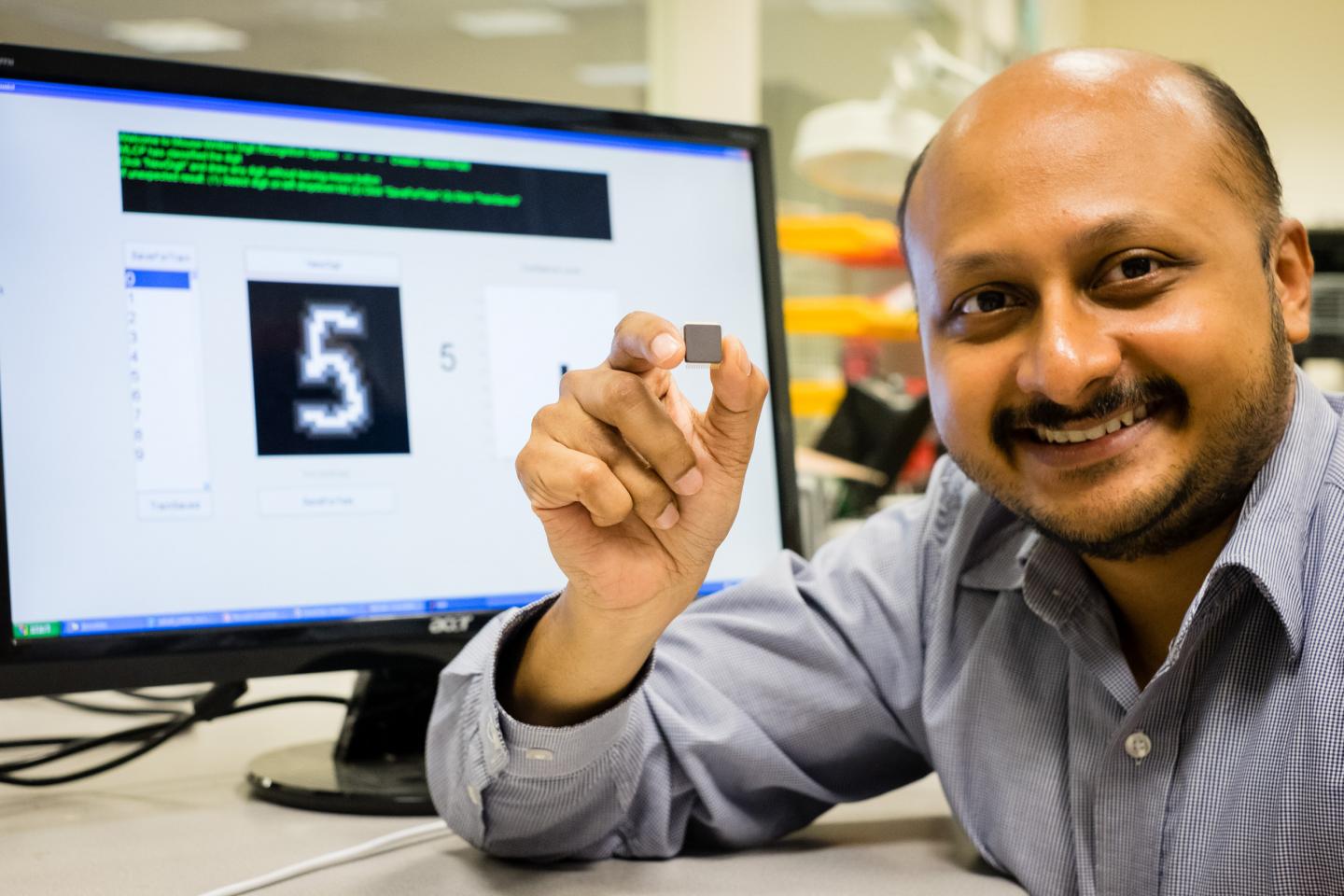
Caption: NTU Asst Prof Arindam Basu is holding his low-powered smart chip. Credit: NTU Singapore

Caption: NTU Asst Prof Arindam Basu is holding his low-powered smart chip. Credit: NTU Singapore

A Feb. 11, 2016 Nanyang Technological University (NTU) press release (also on EurekAlert), which originated the news item, provides more detail,

Scientists at Nanyang Technological University, Singapore (NTU Singapore) have developed a small smart chip that can be paired with neural implants for efficient wireless transmission of brain signals.

Neural implants when embedded in the brain can alleviate the debilitating symptoms of Parkinson’s disease or give paraplegic people the ability to move their prosthetic limbs.

However, they need to be connected by wires to an external device outside the body. For a prosthetic patient, the neural implant is connected to a computer that decodes the brain signals so the artificial limb can move.

These external wires are not only cumbersome but the permanent openings which allow the wires into the brain increases the risk of infections.

The new chip by NTU scientists can allow the transmission of brain data wirelessly and with high accuracy.

Assistant Professor Arindam Basu from NTU’s School of Electrical and Electronic Engineering said the research team have tested the chip on data recorded from animal models, which showed that it could decode the brain’s signal to the hand and fingers with 95 per cent accuracy.

“What we have developed is a very versatile smart chip that can process data, analyse patterns and spot the difference,” explained Prof Basu.

“It is about a hundred times more efficient than current processing chips on the market. It will lead to more compact medical wearable devices, such as portable ECG monitoring devices and neural implants, since we no longer need large batteries to power them.”

Different from other wireless implants

To achieve high accuracy in decoding brain signals, implants require thousands of channels of raw data. To wirelessly transmit this large amount of data, more power is also needed which means either bigger batteries or more frequent recharging.

This is not feasible as there is limited space in the brain for implants while frequent recharging means the implants cannot be used for long-term recording of signals.

Current wireless implant prototypes thus suffer from a lack of accuracy as they lack the bandwidth to send out thousands of channels of raw data.

Instead of enlarging the power source to support the transmission of raw data, Asst Prof Basu tried to reduce the amount of data that needs to be transmitted.

Designed to be extremely power-efficient, NTU’s patented smart chip will analyse and decode the thousands of signals from the neural implants in the brain, before compressing the results and sending it wirelessly to a small external receiver.

This invention and its findings were published last month [December 2015] in the prestigious journal, IEEE Transactions on Biomedical Circuits & Systems, by the Institute of Electrical and Electronics Engineers, the world’s largest professional association for the advancement of technology.

Its underlying science was also featured in three international engineering conferences (two in Atlanta, USA and one in China) over the last three months.

Versatile smart chip with multiple uses

This new smart chip is designed to analyse data patterns and spot any abnormal or unusual patterns.

For example, in a remote video camera, the chip can be programmed to send a video back to the servers only when a specific type of car or something out of the ordinary is detected, such as an intruder.

This would be extremely beneficial for the Internet of Things (IOT), where every electrical and electronic device is connected to the Internet through a smart chip.

With a report by marketing research firm Gartner Inc predicting that 6.4 billion smart devices and appliances will be connected to the Internet by 2016, and will rise to 20.8 billion devices by 2020, reducing network traffic will be a priority for most companies.

Using NTU’s new chip, the devices can process and analyse the data on site, before sending back important details in a compressed package, instead of sending the whole data stream. This will reduce data usage by over a thousand times.

Asst Prof Basu is now in talks with Singapore Technologies Electronics Limited to adapt his smart chip that can significantly reduce power consumption and the amount of data transmitted by battery-operated remote sensors, such as video cameras.

The team is also looking to expand the applications of the chip into commercial products, such as to customise it for smart home sensor networks, in collaboration with a local electronics company.

The chip, measuring 5mm by 5mm can now be licensed by companies from NTU’s commercialisation arm, NTUitive.

Here’s a link to and a citation for the paper,

A 128-Channel Extreme Learning Machine-Based Neural Decoder for Brain Machine Interfaces by Yi Chen, Enyi Yao, Arindam Basu. IEEE Transactions on Biomedical Circuits and Systems, 2015; 1 DOI: 10.1109/TBCAS.2015.2483618

This paper is behind a paywall.

Australia

Earlier this month there was a Feb. 9, 2016 announcement about a planned human clinical trial in Australia for a new brain-machine interface (neural implant). Before proceeding with the news, here’s what this implant looks like,

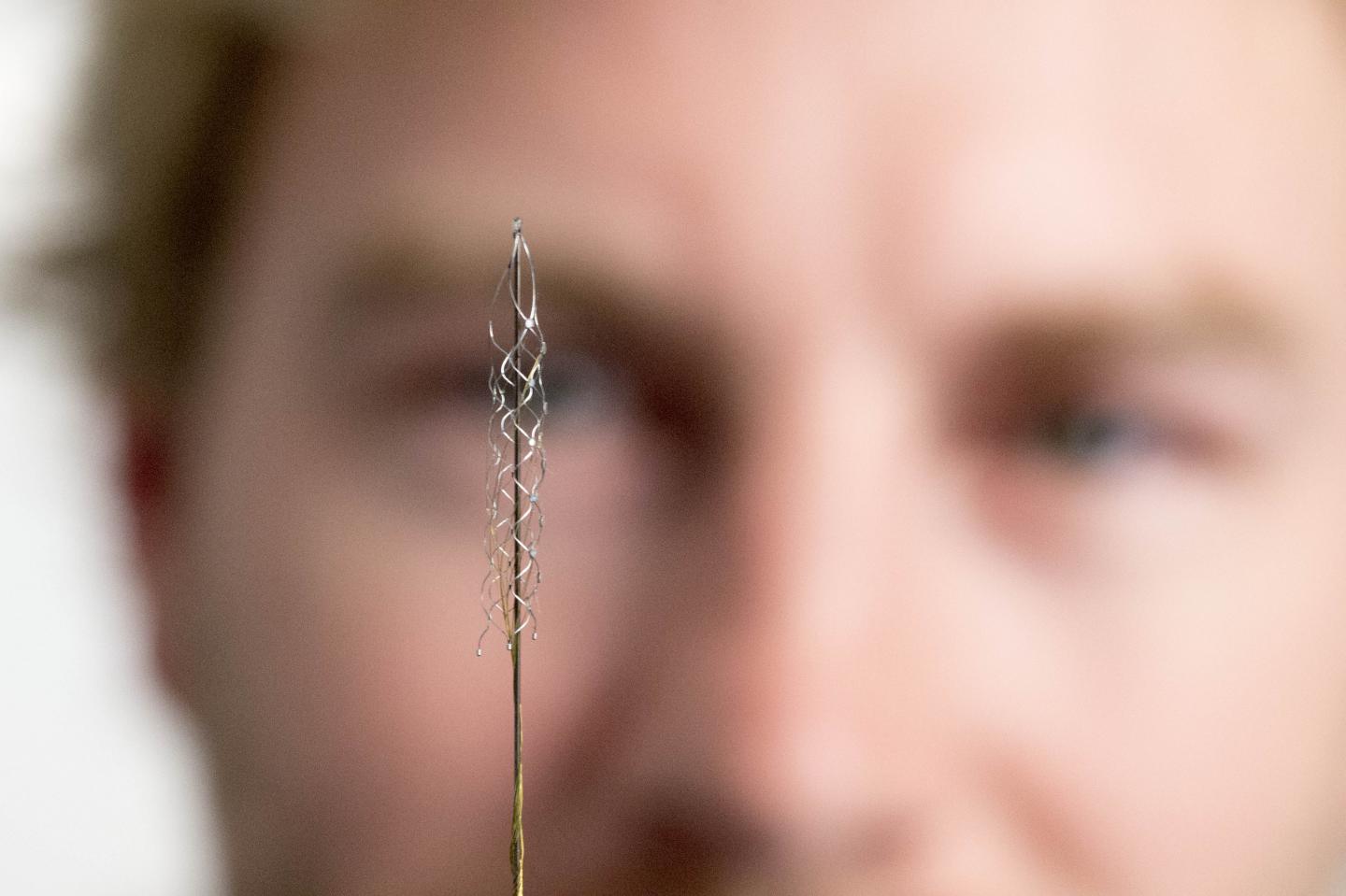
Caption: This tiny device, the size of a small paperclip, is implanted in to a blood vessel next to the brain and can read electrical signals from the motor cortex, the brain's control centre. These signals can then be transmitted to an exoskeleton or wheelchair to give paraplegic patients greater mobility. Users will need to learn how to communicate with their machinery, but over time, it is thought it will become second nature, like driving or playing the piano. The first human trials are slated for 2017 in Melbourne, Australia. Credit: The University of Melbourne.

Caption: This tiny device, the size of a small paperclip, is implanted in to a blood vessel next to the brain and can read electrical signals from the motor cortex, the brain’s control centre. These signals can then be transmitted to an exoskeleton or wheelchair to give paraplegic patients greater mobility. Users will need to learn how to communicate with their machinery, but over time, it is thought it will become second nature, like driving or playing the piano. The first human trials are slated for 2017 in Melbourne, Australia. Credit: The University of Melbourne.

A Feb. 9, 2016 University of Melbourne press release (also on EurekAlert), which originated the news item, provides more detail,

Melbourne medical researchers have created a new minimally invasive brain-machine interface, giving people with spinal cord injuries new hope to walk again with the power of thought.

The brain machine interface consists of a stent-based electrode (stentrode), which is implanted within a blood vessel next to the brain, and records the type of neural activity that has been shown in pre-clinical trials to move limbs through an exoskeleton or to control bionic limbs.

The new device is the size of a small paperclip and will be implanted in the first in-human trial at The Royal Melbourne Hospital in 2017.

The results published today in Nature Biotechnology show the device is capable of recording high-quality signals emitted from the brain’s motor cortex, without the need for open brain surgery.

Principal author and Neurologist at The Royal Melbourne Hospital and Research Fellow at The Florey Institute of Neurosciences and the University of Melbourne, Dr Thomas Oxley, said the stentrode was revolutionary.

“The development of the stentrode has brought together leaders in medical research from The Royal Melbourne Hospital, The University of Melbourne and the Florey Institute of Neuroscience and Mental Health. In total 39 academic scientists from 16 departments were involved in its development,” Dr Oxley said.

“We have been able to create the world’s only minimally invasive device that is implanted into a blood vessel in the brain via a simple day procedure, avoiding the need for high risk open brain surgery.

“Our vision, through this device, is to return function and mobility to patients with complete paralysis by recording brain activity and converting the acquired signals into electrical commands, which in turn would lead to movement of the limbs through a mobility assist device like an exoskeleton. In essence this a bionic spinal cord.”

Stroke and spinal cord injuries are leading causes of disability, affecting 1 in 50 people. There are 20,000 Australians with spinal cord injuries, with the typical patient a 19-year old male, and about 150,000 Australians left severely disabled after stroke.

Co-principal investigator and biomedical engineer at the University of Melbourne, Dr Nicholas Opie, said the concept was similar to an implantable cardiac pacemaker – electrical interaction with tissue using sensors inserted into a vein, but inside the brain.

“Utilising stent technology, our electrode array self-expands to stick to the inside wall of a vein, enabling us to record local brain activity. By extracting the recorded neural signals, we can use these as commands to control wheelchairs, exoskeletons, prosthetic limbs or computers,” Dr Opie said.

“In our first-in-human trial, that we anticipate will begin within two years, we are hoping to achieve direct brain control of an exoskeleton for three people with paralysis.”

“Currently, exoskeletons are controlled by manual manipulation of a joystick to switch between the various elements of walking – stand, start, stop, turn. The stentrode will be the first device that enables direct thought control of these devices”

Neurophysiologist at The Florey, Professor Clive May, said the data from the pre-clinical study highlighted that the implantation of the device was safe for long-term use.

“Through our pre-clinical study we were able to successfully record brain activity over many months. The quality of recording improved as the device was incorporated into tissue,” Professor May said.

“Our study also showed that it was safe and effective to implant the device via angiography, which is minimally invasive compared with the high risks associated with open brain surgery.

“The brain-computer interface is a revolutionary device that holds the potential to overcome paralysis, by returning mobility and independence to patients affected by various conditions.”

Professor Terry O’Brien, Head of Medicine at Departments of Medicine and Neurology, The Royal Melbourne Hospital and University of Melbourne said the development of the stentrode has been the “holy grail” for research in bionics.

“To be able to create a device that can record brainwave activity over long periods of time, without damaging the brain is an amazing development in modern medicine,” Professor O’Brien said.

“It can also be potentially used in people with a range of diseases aside from spinal cord injury, including epilepsy, Parkinsons and other neurological disorders.”

The development of the minimally invasive stentrode and the subsequent pre-clinical trials to prove its effectiveness could not have been possible without the support from the major funding partners – US Defense Department DARPA [Defense Advanced Research Projects Agency] and Australia’s National Health and Medical Research Council.

So, DARPA is helping fund this, eh? Interesting but not a surprise given the agency’s previous investments in brain research and neuroprosthetics.

For those who like to get their news via video,

Here’s a link to and a citation for the paper,

Minimally invasive endovascular stent-electrode array for high-fidelity, chronic recordings of cortical neural activity by Thomas J Oxley, Nicholas L Opie, Sam E John, Gil S Rind, Stephen M Ronayne, Tracey L Wheeler, Jack W Judy, Alan J McDonald, Anthony Dornom, Timothy J H Lovell, Christopher Steward, David J Garrett, Bradford A Moffat, Elaine H Lui, Nawaf Yassi, Bruce C V Campbell, Yan T Wong, Kate E Fox, Ewan S Nurse, Iwan E Bennett, Sébastien H Bauquier, Kishan A Liyanage, Nicole R van der Nagel, Piero Perucca, Arman Ahnood et al. Nature Biotechnology (2016)  doi:10.1038/nbt.3428 Published online 08 February 2016

This paper is behind a paywall.

I wish the researchers in Singapore, Australia, and elsewhere, good luck!

*’Sinagpore’ in head changed to ‘Singapore’ on May 14, 2019.

Brain-like computing with optical fibres

Researchers from Singapore and the United Kingdom are exploring an optical fibre approach to brain-like computing (aka neuromorphic computing) as opposed to approaches featuring a memristor or other devices such as a nanoionic device that I’ve written about previously. A March 10, 2015 news item on Nanowerk describes this new approach,

Computers that function like the human brain could soon become a reality thanks to new research using optical fibres made of speciality glass.

Researchers from the Optoelectronics Research Centre (ORC) at the University of Southampton, UK, and Centre for Disruptive Photonic Technologies (CDPT) at the Nanyang Technological University (NTU), Singapore, have demonstrated how neural networks and synapses in the brain can be reproduced, with optical pulses as information carriers, using special fibres made from glasses that are sensitive to light, known as chalcogenides.

“The project, funded under Singapore’s Agency for Science, Technology and Research (A*STAR) Advanced Optics in Engineering programme, was conducted within The Photonics Institute (TPI), a recently established dual institute between NTU and the ORC.”

A March 10, 2015 University of Southampton press release (also on EurekAlert), which originated the news item, describes the nature of the problem that the scientists are trying address (Note: A link has been removed),

Co-author Professor Dan Hewak from the ORC, says: “Since the dawn of the computer age, scientists have sought ways to mimic the behaviour of the human brain, replacing neurons and our nervous system with electronic switches and memory. Now instead of electrons, light and optical fibres also show promise in achieving a brain-like computer. The cognitive functionality of central neurons underlies the adaptable nature and information processing capability of our brains.”

In the last decade, neuromorphic computing research has advanced software and electronic hardware that mimic brain functions and signal protocols, aimed at improving the efficiency and adaptability of conventional computers.

However, compared to our biological systems, today’s computers are more than a million times less efficient. Simulating five seconds of brain activity takes 500 seconds and needs 1.4 MW of power, compared to the small number of calories burned by the human brain.

Using conventional fibre drawing techniques, microfibers can be produced from chalcogenide (glasses based on sulphur) that possess a variety of broadband photoinduced effects, which allow the fibres to be switched on and off. This optical switching or light switching light, can be exploited for a variety of next generation computing applications capable of processing vast amounts of data in a much more energy-efficient manner.

Co-author Dr Behrad Gholipour explains: “By going back to biological systems for inspiration and using mass-manufacturable photonic platforms, such as chalcogenide fibres, we can start to improve the speed and efficiency of conventional computing architectures, while introducing adaptability and learning into the next generation of devices.”

By exploiting the material properties of the chalcogenides fibres, the team led by Professor Cesare Soci at NTU have demonstrated a range of optical equivalents of brain functions. These include holding a neural resting state and simulating the changes in electrical activity in a nerve cell as it is stimulated. In the proposed optical version of this brain function, the changing properties of the glass act as the varying electrical activity in a nerve cell, and light provides the stimulus to change these properties. This enables switching of a light signal, which is the equivalent to a nerve cell firing.

The research paves the way for scalable brain-like computing systems that enable ‘photonic neurons’ with ultrafast signal transmission speeds, higher bandwidth and lower power consumption than their biological and electronic counterparts.

Professor Cesare Soci said: “This work implies that ‘cognitive’ photonic devices and networks can be effectively used to develop non-Boolean computing and decision-making paradigms that mimic brain functionalities and signal protocols, to overcome bandwidth and power bottlenecks of traditional data processing.”

Here’s a link to and a citation for the paper,

Amorphous Metal-Sulphide Microfibers Enable Photonic Synapses for Brain-Like Computing by Behrad Gholipour, Paul Bastock, Chris Craig, Khouler Khan, Dan Hewak. and Cesare Soci. Advanced Optical Materials DOI: 10.1002/adom.201400472
Article first published online: 15 JAN 2015

© 2015 WILEY-VCH Verlag GmbH & Co. KGaA, Weinheim

This article is behind a paywall.

For anyone interested in memristors and nanoionic devices, here are a few posts (from this blog) to get you started:

Memristors, memcapacitors, and meminductors for faster computers (June 30, 2014)

This second one offers more details and links to previous pieces,

Memristor, memristor! What is happening? News from the University of Michigan and HP Laboratories (June 25, 2014)

This post is more of a survey including memristors, nanoionic devices, ‘brain jelly, and more,

Brain-on-a-chip 2014 survey/overview (April 7, 2014)

One comment, this brain-on-a-chip is not to be confused with ‘organs-on-a-chip’ projects which are attempting to simulate human organs (Including the brain) so chemicals and drugs can be tested.

Nanomedicine living up to its promise?

Michael Berger has written a March 10, 2015 Nanowerk spotlight article reviewing nanomedicine’s  progress or lack thereof (Note: Links have been removed),

In early 2003, the European Science Foundation launched its Scientific Forward Look on Nanomedicine, a foresight study (report here ;pdf) and in 2004, the U.S. National Institute[s] of Health (NIH) published its Roadmap (now Common Fund) of the Nanomedicine Initiative. This program began in 2005 with a national network of eight Nanomedicine Development Centers. Now, in the second half of this 10-year program, the four centers best positioned to effectively apply their findings to translational studies were selected to continue receiving support.

A generally accepted definition of nanomedicine refers to highly specific medical intervention at the molecular scale for curing disease or repairing damaged tissues, such as bone, muscle, or nerve.

Much of Berger’s article is based on Subbu Venkatraman’s, Director of the NTU (Nanyang Technological University)-Northwestern Nanomedicine Institute in Singapore, paper, Has nanomedicine lived up to its promise?, 2014 Nanotechnology 25 372501 doi:10.1088/0957-4484/25/37/372501 (Note: Links have been removed),

… Historically, the approval of Doxil as the very first nanotherapeutic product in 1995 is generally regarded as the dawn of nanomedicine for human use. Since then, research activity in this area has been frenetic, with, for example, 2000 patents being generated in 2003, in addition to 1200 papers [2]. In the same time period, a total of 207 companies were involved in developing nanomedicinal products in diagnostics, imaging, drug delivery and implants. About 38 products loosely classified as nanomedicine products were in fact approved by 2004. Out of these, however, a number of products (five in all) were based on PEG-ylated proteins, which strictly speaking, are not so much nanomedicine products as molecular therapeutics. Nevertheless, the promise of nanomedicine was being translated into funding for small companies, and into clinical success, so that by 2013, the number of approved products had reached 54 in all, with another 150 in various stages of clinical trials [3]. The number of companies and institutions had risen to 241 (including research centres that were working on nanomedicine). A PubMed search on articles relating to nanomedicine shows 7400 hits over 10 years, of which 1874 were published in 2013 alone. Similarly, the US patent office database shows 409 patents (since 1976) that were granted in nanomedicine, with another 679 applications awaiting approval. So judging by research activity and funding the field of nanomedicine has been very fertile; however, when we use the yardstick of clinical success and paradigm shifts in treatment, the results appear more modest.

Both Berger’s spotlight article and Venkatraman’s review provide interesting reading and neither is especially long.