It seems to me that I stumbled across quite a few carbon nanotube (CNT) stories in 2018. This one comes courtesy of Japan (from a June 28, 2018 news item on Nanowerk),
Researchers at Tokyo Tech have developed flexible terahertz imagers based on chemically “tunable” carbon nanotube materials. The findings expand the scope of terahertz applications to include wrap-around, wearable technologies as well as large-area photonic devices.
Here’s a peek at an imager,
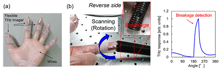
Figure 1. The CNT-based flexible THz imager (a) Resting on a fingertip, the CNT THz imager can easily wrap around curved surfaces. (b) Just by inserting and rotating a flexible THz imager attached to the fingertip, damage to a pipe was clearly detected. Courtesy Tokyo Tech
A June 28, 2018 Tokyo Tech Institute press release (also on Eurekalert), which originated the news item, provides more detail,
Carbon nanotubes (CNTs) are beginning to take the electronics world by storm, and now their use in terahertz (THz) technologies has taken a big step forward.
Due to their excellent conductivity and unique physical properties, CNTs are an attractive option for next-generation electronic devices. One of the most promising developments is their application in THz devices. Increasingly, THz imagers are emerging as a safe and viable alternative to conventional imaging systems across a wide range of applications, from airport security, food inspection and art authentication to medical and environmental sensing technologies.
The demand for THz detectors that can deliver real-time imaging for a broad range of industrial applications has spurred research into low-cost, flexible THz imaging systems. Yukio Kawano of the Laboratory for Future Interdisciplinary Research of Science and Technology, Tokyo Tech, is a world-renowned expert in this field. In 2016, for example, he announced the development of wearable terahertz technologies based on multiarrayed carbon nanotubes.
Kawano and his team have since been investigating THz detection performance for various types of CNT materials, in recognition of the fact that there is plenty of room for improvement to meet the needs of industrial-scale applications.
Now, they report the development of flexible THz imagers for CNT films that can be fine-tuned to maximize THz detector performance.
Publishing their findings in ACS Applied Nano Materials, the new THz imagers are based on chemically adjustable semiconducting CNT films.
By making use of a technology known as ionic liquid gating1, the researchers demonstrated that they could obtain a high degree of control over key factors related to THz detector performance for a CNT film with a thickness of 30 micrometers. This level of thickness was important to ensure that the imagers would maintain their free-standing shape and flexibility, as shown in Figure 1 [see above].
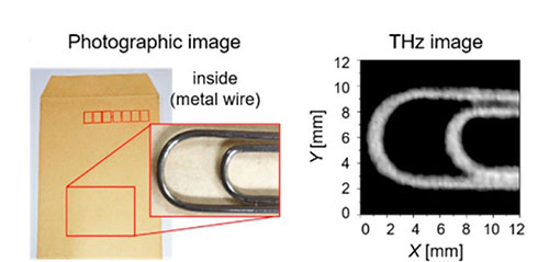
“Additionally,” the team says, “we developed gate-free Fermi-level2 tuning based on variable-concentration dopant solutions and fabricated a Fermi-level-tuned p-n junction3 CNT THz imager.” In experiments using this new type of imager, the researchers achieved successful visualization of a metal paper clip inside a standard envelope (see Figure 2.)
Figure 2. Non-contact, non-destructive visualization
The CNT THz imager enabled clear, non-destructive visualization of a metal paper clip inside an envelope.
The bendability of the new THz imager and the possibility of even further fine-tuning will expand the range of CNT-based devices that could be developed in the near future.
Moreover, low-cost fabrication methods such as inkjet coating could make large-area THz imaging devices more readily available.
A technique used to modulate a material’s charge carrier properties.
A measure of the electrochemical potential for electrons, which is important for determining the electrical and thermal properties of solids. The term is named after the Italian–American physicist Enrico Fermi.
Refers to the interface between positive (p-type) and negative (n-type) semiconducting materials. These junctions form the basis of semiconductor electronic devices.
Here’s a link to and a citation for the paper,
Fermi-Level-Controlled Semiconducting-Separated Carbon Nanotube Films for Flexible Terahertz Imagers by Daichi Suzuki, Yuki Ochiai, Yota Nakagawa, Yuki Kuwahara, Takeshi Saito, and Yukio Kawano. ACS Appl. Nano Mater., 2018, 1 (6), pp 2469–2475 DOI: 10.1021/acsanm.8b00421 Publication Date (Web): June 6, 2018
Copyright © 2018 American Chemical Society
This paper is behind a paywall.