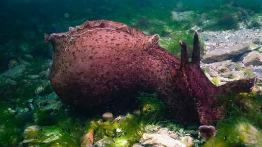
I don’t think I’ve ever seen a picture of a sea slug before. Its appearance reminds me of its terrestrial cousin.
As for some of the latest news on brainlike computing, a December 7, 2021 news item on Nanowerk makes an announcement from the Argonne National Laboratory (a US Department of Energy laboratory; Note: Links have been removed),
A team of scientists has discovered a new material that points the way toward more efficient artificial intelligence hardware for everything from self-driving cars to surgical robots.
For artificial intelligence (AI) to get any smarter, it needs first to be as intelligent as one of the simplest creatures in the animal kingdom: the sea slug.
A new study has found that a material can mimic the sea slug’s most essential intelligence features. The discovery is a step toward building hardware that could help make AI more efficient and reliable for technology ranging from self-driving cars and surgical robots to social media algorithms.
The study, published in the Proceedings of the National Academy of Sciences [PNAS] (“Neuromorphic learning with Mott insulator NiO”), was conducted by a team of researchers from Purdue University, Rutgers University, the University of Georgia and the U.S. Department of Energy’s (DOE) Argonne National Laboratory. The team used the resources of the Advanced Photon Source (APS), a DOE Office of Science user facility at Argonne.
A December 6, 2021 Argonne National Laboratory news release (also on EurekAlert) by Kayla Wiles and Andre Salles, which originated the news item, provides more detail,
“Through studying sea slugs, neuroscientists discovered the hallmarks of intelligence that are fundamental to any organism’s survival,” said Shriram Ramanathan, a Purdue professor of Materials Engineering. “We want to take advantage of that mature intelligence in animals to accelerate the development of AI.”
Two main signs of intelligence that neuroscientists have learned from sea slugs are habituation and sensitization. Habituation is getting used to a stimulus over time, such as tuning out noises when driving the same route to work every day. Sensitization is the opposite — it’s reacting strongly to a new stimulus, like avoiding bad food from a restaurant.
AI has a really hard time learning and storing new information without overwriting information it has already learned and stored, a problem that researchers studying brain-inspired computing call the “stability-plasticity dilemma.” Habituation would allow AI to “forget” unneeded information (achieving more stability) while sensitization could help with retaining new and important information (enabling plasticity).
In this study, the researchers found a way to demonstrate both habituation and sensitization in nickel oxide, a quantum material. Quantum materials are engineered to take advantage of features available only at nature’s smallest scales, and useful for information processing. If a quantum material could reliably mimic these forms of learning, then it may be possible to build AI directly into hardware. And if AI could operate both through hardware and software, it might be able to perform more complex tasks using less energy.
“We basically emulated experiments done on sea slugs in quantum materials toward understanding how these materials can be of interest for AI,” Ramanathan said.
Neuroscience studies have shown that the sea slug demonstrates habituation when it stops withdrawing its gill as much in response to tapping. But an electric shock to its tail causes its gill to withdraw much more dramatically, showing sensitization.
For nickel oxide, the equivalent of a “gill withdrawal” is an increased change in electrical resistance. The researchers found that repeatedly exposing the material to hydrogen gas causes nickel oxide’s change in electrical resistance to decrease over time, but introducing a new stimulus like ozone greatly increases the change in electrical resistance.
Ramanathan and his colleagues used two experimental stations at the APS to test this theory, using X-ray absorption spectroscopy. A sample of nickel oxide was exposed to hydrogen and oxygen, and the ultrabright X-rays of the APS were used to see changes in the material at the atomic level over time.
“Nickel oxide is a relatively simple material,” said Argonne physicist Hua Zhou, a co-author on the paper who worked with the team at beamline 33-ID. “The goal was to use something easy to manufacture, and see if it would mimic this behavior. We looked at whether the material gained or lost a single electron after exposure to the gas.”
The research team also conducted scans at beamline 29-ID, which uses softer X-rays to probe different energy ranges. While the harder X-rays of 33-ID are more sensitive to the “core” electrons, those closer to the nucleus of the nickel oxide’s atoms, the softer X-rays can more readily observe the electrons on the outer shell. These are the electrons that define whether a material is conductive or resistive to electricity.
“We’re very sensitive to the change of resistivity in these samples,” said Argonne physicist Fanny Rodolakis, a co-author on the paper who led the work at beamline 29-ID. “We can directly probe how the electronic states of oxygen and nickel evolve under different treatments.”
Physicist Zhan Zhang and postdoctoral researcher Hui Cao, both of Argonne, contributed to the work, and are listed as co-authors on the paper. Zhang said the APS is well suited for research like this, due to its bright beam that can be tuned over different energy ranges.
For practical use of quantum materials as AI hardware, researchers will need to figure out how to apply habituation and sensitization in large-scale systems. They also would have to determine how a material could respond to stimuli while integrated into a computer chip.
This study is a starting place for guiding those next steps, the researchers said. Meanwhile, the APS is undergoing a massive upgrade that will not only increase the brightness of its beams by up to 500 times, but will allow for those beams to be focused much smaller than they are today. And this, Zhou said, will prove useful once this technology does find its way into electronic devices.
“If we want to test the properties of microelectronics,” he said, “the smaller beam that the upgraded APS will give us will be essential.”
In addition to the experiments performed at Purdue and Argonne, a team at Rutgers University performed detailed theory calculations to understand what was happening within nickel oxide at a microscopic level to mimic the sea slug’s intelligence features. The University of Georgia measured conductivity to further analyze the material’s behavior.
A version of this story was originally published by Purdue University
About the Advanced Photon Source
The U. S. Department of Energy Office of Science’s Advanced Photon Source (APS) at Argonne National Laboratory is one of the world’s most productive X-ray light source facilities. The APS provides high-brightness X-ray beams to a diverse community of researchers in materials science, chemistry, condensed matter physics, the life and environmental sciences, and applied research. These X-rays are ideally suited for explorations of materials and biological structures; elemental distribution; chemical, magnetic, electronic states; and a wide range of technologically important engineering systems from batteries to fuel injector sprays, all of which are the foundations of our nation’s economic, technological, and physical well-being. Each year, more than 5,000 researchers use the APS to produce over 2,000 publications detailing impactful discoveries, and solve more vital biological protein structures than users of any other X-ray light source research facility. APS scientists and engineers innovate technology that is at the heart of advancing accelerator and light-source operations. This includes the insertion devices that produce extreme-brightness X-rays prized by researchers, lenses that focus the X-rays down to a few nanometers, instrumentation that maximizes the way the X-rays interact with samples being studied, and software that gathers and manages the massive quantity of data resulting from discovery research at the APS.
This research used resources of the Advanced Photon Source, a U.S. DOE Office of Science User Facility operated for the DOE Office of Science by Argonne National Laboratory under Contract No. DE-AC02-06CH11357.
Argonne National Laboratory seeks solutions to pressing national problems in science and technology. The nation’s first national laboratory, Argonne conducts leading-edge basic and applied scientific research in virtually every scientific discipline. Argonne researchers work closely with researchers from hundreds of companies, universities, and federal, state and municipal agencies to help them solve their specific problems, advance America’s scientific leadership and prepare the nation for a better future. With employees from more than 60 nations, Argonne is managed by UChicago Argonne, LLC for the U.S. Department of Energy’s Office of Science.
The U.S. Department of Energy’s Office of Science is the single largest supporter of basic research in the physical sciences in the United States and is working to address some of the most pressing challenges of our time. For more information, visit https://energy.gov/science.
You can find the September 24, 2021 Purdue University story, Taking lessons from a sea slug, study points to better hardware for artificial intelligence here.
Here’s a link to and a citation for the paper,
Neuromorphic learning with Mott insulator NiO by Zhen Zhang, Sandip Mondal, Subhasish Mandal, Jason M. Allred, Neda Alsadat Aghamiri, Alireza Fali, Zhan Zhang, Hua Zhou, Hui Cao, Fanny Rodolakis, Jessica L. McChesney, Qi Wang, Yifei Sun, Yohannes Abate, Kaushik Roy, Karin M. Rabe, and Shriram Ramanathan. PNAS September 28, 2021 118 (39) e2017239118 DOI: https://doi.org/10.1073/pnas.2017239118
This paper is behind a paywall.