Tag Archives: single-walled carbon nanotubes

“Control my chirality, please,” said the carbon nanotube to the researchers

A combined Finnish, Russian, and Danish team have found a way to control the chirality of single-walled carbon nanotubes according to an Apr. 30, 2013 news item on Azonano,

An ultimate goal in the field of carbon nanotube research is to synthesise single-walled carbon nanotubes (SWNTs) with controlled chiralities. Twenty years after the discovery of SWNTs, scientists from Aalto University in Finland, A.M. Prokhorov General Physics Institute RAS in Russia and the Center for Electron Nanoscopy of Technical University of Denmark (DTU) have managed to control chirality in carbon nanotubes during their chemical vapor deposition synthesis.

The Aalto University Apr. 29, 2013 news release, which originated the news item, goes on to explain,

 Over the years, substantial progress has been made to develop various structure-controlled synthesis methods. However, precise control over the chiral structure of SWNTs has been largely hindered by a lack of practical means to direct the formation of the metal nanoparticle catalysts and their catalytic dynamics during tube growth.

– We achieved an epitaxial formation of Co nanoparticles by reducing a well-developed solid solution in CO, reveals Maoshuai He, a postdoctoral researcher at Aalto University School of Chemical Technology.

– For the first time, the new catalyst was employed for selective growth of SWNTs, adds senior staff scientist Hua Jiang from Aalto University School of Science.

By introducing the new catalysts into a conventional CVD reactor, the research team demonstrated preferential growth of semiconducting SWNTs (~90%) with an exceptionally high population of (6,5) tubes (53%) at 500 °C. Furthermore, they also showed a shift of the chiral preference from (6,5) tubes at 500 °C  to (7, 6) and (9, 4) nanotubes at 400 °C.

– These findings open new perspectives both for structural control of SWNTs and for elucidating their growth mechanisms, thus are important for the fundamental understanding of science behind nanotube growth, comments Professor Juha Lehtonen from Aalto University.

For anyone like me who needs a description of chirality, there’s this from Wikipedia,

Chirality (pron.: /kaɪˈrælɪtiː/) is a property of asymmetry important in several branches of science. The word chirality is derived from the Greek, χειρ (kheir), “hand”, a familiar chiral object.

An object or a system is chiral if it is not identical to its mirror image, that is, it cannot be superposed onto it. A chiral object and its mirror image are called enantiomorphs (Greek opposite forms) or, when referring to molecules, enantiomers. A non-chiral object is called achiral (sometimes also amphichiral) and can be superposed on its mirror image.

Human hands are perhaps the most universally recognized example of chirality: The left hand is a non-superimposable mirror image of the right hand; no matter how the two hands are oriented, it is impossible for all the major features of both hands to coincide.[2] This difference in symmetry becomes obvious if someone attempts to shake the right hand of a person using his left hand, or if a left-handed glove is placed on a right hand. In mathematics chirality is the property of a figure that is not identical to its mirror image.

One of the researchers notes why they, or anyone else, would want to control the chirality of carbon nanotubes, from the news release,

– Chirality defines the optical and electronic properties of carbon nanotubes, so controlling it is a key to exploiting their practical applications, says Professor Esko I. Kauppinen, the leader of the Nanomaterials Group in Aalto University School of Science.

ETA Apr. 30, 2013 at 4:20 pm PDT: Here’s a link to and a citation for the team’s published paper,

Chiral-Selective Growth of Single-Walled Carbon Nanotubes on Lattice-Mismatched Epitaxial Cobalt Nanoparticles by Maoshuai He, Hua Jiang, Bilu Liu, Pavel V. Fedotov, Alexander I. Chernov, Elena D. Obraztsova, Filippo Cavalca, Jakob B. Wagner, Thomas W. Hansen, Ilya V. Anoshkin, Ekaterina A. Obraztsova, Alexey V. Belkin, Emma Sairanen, Albert G. Nasibulin,  Juha Lehtonen, & Esko I. Kauppinen. Scientific Reports 3, Article number 1460  doi:10.1038/srep01460 Published15 March 2013

This article is open access.
Morpho butterflies detect heat for GE

One wonders if Morpho butterflies are going to decide that they need to protect their intellectual property. Yet another scientific group has found a way to exploit the nanostructures on the Morpho butterfly’s wing.  From the Feb. 13, 2012 news item on Nanowerk,

GE [General Electric] scientists are exploring many potential thermal imaging and sensing applications with their new detection concept such as medical diagnostics, surveillance, non-destructive inspection and others, where visual heat maps of imaged areas serve as a valuable condition indicator. Some examples include:

  • Thermal Imaging for advanced medical diagnosis – to better visualize inflammation in the body and understand changes in a patient’s health earlier.
  • Advanced thermal vision – to see things at night and during the day in much greater detail than what is possible today.
  • Fire thermal Imaging – to aid firefighters with new handheld devices to enhance firefighter safety in operational situations
  • Thermal security surveillance – to improve public safety and homeland protection
  • Thermal characterization of wound infections – to facilitate early diagnosis.

“The iridescence of Morpho butterflies has inspired our team for yet another technological opportunity. This time we see the potential to develop the next generation of thermal imaging sensors that deliver higher sensitivity and faster response times in a more simplified, cost-effective design,” said Dr. Radislav Potyrailo, Principal Scientist at GE Global Research who leads GE’s bio-inspired photonics programs. “This new class of thermal imaging sensors promises significant improvements over existing detectors in their image quality, speed, sensitivity, size, power requirements, and cost.”

GE has provided a video and description that illustrates this newest biomimicry work. First the description then the video (from http://www.youtube.com/watch?v=UoaILSCzlTo&feature=youtu.be)

This is a thermographic video of a Morpho butterfly structure in response to heat pulses produced by breathing onto the whole butterfly structure (video part 1) and onto its localized areas (video part 2). Nanostructures on Morpho butterfly wings coated with carbon nanotubes can sense temperature chances down to .02 degrees Celsius, at a response rate of 1/40 of a second. This is a demonstration of how new bio-inspired designs by GE scientists could enable more advanced applications for industrial inspection, medical diagnostics and military. This video was filmed by Bryan Whalen in the Electronics Cooling Lab at GE Global Research.

This newest work seems to have its origins in a DARPA-funded (US Defense Advanced Research Projects Agency) GE project. From the Aug. 12, 2010 GE news release,

Scientists at GE Global Research, GE’s technology development arm, in collaboration with Air Force Research Laboratory, State University at Albany, and University of Exeter, have received a four-year, $6.3 million award from the Defense Advanced Research Projects Agency (DARPA) to develop new bio-inspired nanostructured sensors that would enable faster, more selective detection of dangerous warfare agents and explosives.

Three years ago, GE scientists discovered that nanostructures from wing scales of butterflies exhibited acute chemical sensing properties. [emphasis bold] Since then, GE scientists have been developing a dynamic, new sensing platform that replicates these unique properties.  Recognizing the potential of GE’s sensing technologies for improving homeland protection, DARPA is supporting further research. [emphasis mine]

For anyone who’s particularly interested in the technical details, Dexter Johnson offers more in his Feb. 13, 2012 posting about this research on the Nanoclast blog for the IEEE (Institute of Electrical and Electronics Engineers).

Sticky tape and carbon nanotubes

I like the use of simple, homely tools in science and the use of sticky tape (or scotch tape) to isolate graphene by Andre Geim and Konstantin Novoselov for work that led to a Nobel prize certainly fits that category.

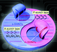
Scientists inspired by the ‘sticky tape technique’ for separating graphene from graphite (you can view a video which shows you how to do this at home using a lead pencil in my November 26, 2010 posting) have devised a nondamaging means of separating metallic and semiconducting single-walled carbon nanotubes. From the abstract for the paper, Separation of Metallic and Semiconducting Single-Walled Carbon Nanotube Arrays by “Scotch Tape” (the paper is behind a paywall),

Amine-functionalized A-scotch tape selectively removes s(semiconducting)-SWNTs, the phenyl-functionalized P-scotch tape acts specifically towards m (metallic)-SWNTs.

From the Sept. 12, 2011 news item on Nanowerk,

The researchers used thin films of polydimethylsiloxane (PDMS) chemically modified with either amino or phenyl groups as a type of scotch tape to lift CNTs from the sapphire substrate on which they were prepared (see image). The amino-type scotch tape selectively removes semiconducting CNTs from a mixture of CNTs on the substrate surface, whereas the phenyl-type scotch tape selectively removes only metallic CNTs, without disturbing the CNTs left behind. “Compared with current separation methods based on selective adsorption, we have successfully extended the mechanism to a long nanotube system and controlled the formation of carbon nanotubes perfectly,” says Zhang [Jin Zhang].

If they can find a way to make this technique more productive (only a small number of carbon nanotubes can be separated at this time), then there is great potential for their use in solar cells and other such devices.

Cutting carbon nanotubes

I’ve been meaning to get to this news item about cutting carbon nanotubes for a few days. From the Dec. 17, 2010 news item on Nanowerk,

“We can now design the cutting rate and the diameters we want to cut,” said Kyung-Suk Kim, professor of engineering in the School of Engineering at Brown and the corresponding author on the paper.

The basics of carbon nanotube manufacturing are known. Single-atom thin graphene sheets are immersed in solution (usually water), causing them to look like a plate of tangled spaghetti. The jumbled bundle of nanotubes is then blasted by high-intensity sound waves that create cavities (or partial vacuums) in the solution. The bubbles that arise from these cavities expand and collapse so violently that the heat in each bubble’s core can reach more than 5,000 degrees Kelvin, close to the temperature on the surface of the sun. Meanwhile, each bubble compresses at an acceleration 100 billion times greater than gravity. Considering the terrific energy involved, it’s hardly surprising that the tubes come out at random lengths. Technicians use sieves to get tubes of the desired length. The technique is inexact partly because no one was sure what caused the tubes to fracture.

German researchers had hypothesized that the tube fractures were due to the action of sonic boomlets yanking the tubes apart violently (like taking hold of the two opposite ends of a rope and pulling the rope apart from each end so that it breaks somewhere along its length). Apparently, this was not the case,

They [researchers from Brown University and Korea Institute of Science and Technology] found that rather than being pulled apart, as the German researchers had thought, the tubes were being compressed mightily from both ends. This caused a buckling in a roughly five-nanometer section along the tubes called the compression-concentration zone. In that zone, the tube is twisted into alternating 90-degree-angle folds, so that it fairly resembles a helix.

That discovery still did not explain fully how the tubes are cut. Through more computerized simulations, the group learned the mighty force exerted by the bubbles’ sonic booms caused atoms to be shot off the tube’s lattice-like foundation like bullets from a machine gun.

“It’s almost as if an orange is being squeezed, and the liquid is shooting out sideways,” Kim said. “This kind of fracture by compressive atom ejection has never been observed before in any kind of materials.”

Here’s where the paper was published and why they hope this is an important discovery,

In a paper published this month in the British journal Proceedings of the Royal Society A, researchers at Brown University and in Korea document for the first time how single-walled carbon nanotubes are cut, a finding that could lead to producing more precise, higher-quality nanotubes. Such manufacturing improvements likely would make the nanotubes more attractive for use in automotive, biomedicine, electronics, energy, optics and many other fields.

I didn’t see any projections for when these “more precise, higher-quality nanotubes” might reach the marketplace. It seems to me that they aren’t that sure about the prospects.

Textiles used as batteries at UC Berkeley; University of Calgary, quantum entanglement and building blocks; Raymor Industries has a nano problem with its shareholders?

There seems to be a race to get our clothes electrified so we can become portable recharging devices. From the news item on Azonano,

In research that gives literal meaning to the term “power suit,” University of California, Berkeley, engineers have created energy-scavenging nanofibers that could one day be woven into clothing and textiles.

These nano-sized generators have “piezoelectric” properties that allow them to convert into electricity the energy created through mechanical stress, stretches and twists.

“This technology could eventually lead to wearable ‘smart clothes’ that can power hand-held electronics through ordinary body movements,” said Liwei Lin, UC Berkeley professor of mechanical engineering and head of the international research team that developed the fiber nanogenerators.

This announcement is on the heels of a similar announcement (noted in my posting of Jan.22.10 here)  from researchers at the University of Stanford in California.

Meanwhile, scientists at the University of Calgary are playing with construction toys (they use the lego metaphor, which seems quite popular right now). From the news release on the University of Calgary website (thanks to Azonano where I first found notice of the item),

While many of us enjoyed constructing little houses out of toy bricks, this task is much more difficult if the bricks are elementary particles. It is even harder if these are particles of light—photons—which can only exist while flying at an incredible speed and vanish if they touch anything.

Yet a team at the University of Calgary has accomplished exactly that. By manipulating a mysterious quantum property of light known as entanglement, they are able to mount up to two photons on top of one another to construct a variety of quantum states of light—that is, build two-story quantum toy houses of any style and architecture.

The research has just (yesterday, Feb.14.10) been published in Nature Photonics. You can read the abstract (here after you scroll down) but the rest of the article is behind a paywall.

I found something rather odd this morning about Raymor Industries. It’s a Canadian nanotechnology company (their products are based on single-walled carbon nanotubes) traded on the TSX that is currently experiencing difficulty with, at least some, shareholders. From the item on PRNewsWire,

RAYMOR INDUSTRIES INC. (TSX Venture RAR, RAYRF) is a leading Canadian developer of high technology and a producer of advanced materials and nanomaterials for high value-added applications. Raymor holds the exclusive rights to more than 20 patents throughout the world, with other patents pending. Shareholders have formed a group to fight to protect our shareholder rights and prevent the current board of directors from delisting and the eliminating the common shares of the corporation.  The group is called The Raymor Investors Special Action Group.  The group is sending out this communication to get the attention of the 8000 shareholders and advise them that an appeal to the recent January 27, 2010 court ruling has been launched and is underway.  A strong and reasonable chance exists that the appeal can be won.

If you’re curious about the company and its products, you can read more here at their website, although they offer no additional information about the contretemps.