They should have declared Jan. 25, 2016 ‘L. Mahadevan Day’ at Harvard University. The researcher was listed as an author on two major papers. I covered the first piece of research, 4D printed hydrogels, in this Jan. 26, 2016 posting. Now for Mahadevan’s other work, from a Jan. 27, 2016 news item on Nanotechnology Now,
What if you could make any object out of a flat sheet of paper?
That future is on the horizon thanks to new research by L. Mahadevan, the Lola England de Valpine Professor of Applied Mathematics, Organismic and Evolutionary Biology, and Physics at the Harvard John A. Paulson School of Engineering and Applied Sciences (SEAS). He is also a core faculty member of the Wyss Institute for Biologically Inspired Engineering, and member of the Kavli Institute for Bionano Science and Technology, at Harvard University.
Mahadevan and his team have characterized a fundamental origami fold, or tessellation, that could be used as a building block to create almost any three-dimensional shape, from nanostructures to buildings. …
A Jan. 26, 2016 Harvard University news release by Leah Burrows, which originated the news item, provides more detail about the specific fold the team has been investigating,
The folding pattern, known as the Miura-ori, is a periodic way to tile the plane using the simplest mountain-valley fold in origami. It was used as a decorative item in clothing at least as long ago as the 15th century. A folded Miura can be packed into a flat, compact shape and unfolded in one continuous motion, making it ideal for packing rigid structures like solar panels. It also occurs in nature in a variety of situations, such as in insect wings and certain leaves.
“Could this simple folding pattern serve as a template for more complicated shapes, such as saddles, spheres, cylinders, and helices?” asked Mahadevan.
“We found an incredible amount of flexibility hidden inside the geometry of the Miura-ori,” said Levi Dudte, graduate student in the Mahadevan lab and first author of the paper. “As it turns out, this fold is capable of creating many more shapes than we imagined.”
Think surgical stents that can be packed flat and pop-up into three-dimensional structures once inside the body or dining room tables that can lean flat against the wall until they are ready to be used.
“The collapsibility, transportability and deployability of Miura-ori folded objects makes it a potentially attractive design for everything from space-bound payloads to small-space living to laparoscopic surgery and soft robotics,” said Dudte.
Here’s a .gif demonstrating the fold,
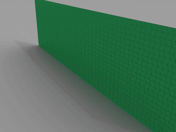
This spiral folds rigidly from flat pattern through the target surface and onto the flat-folded plane (Image courtesy of Mahadevan Lab) Harvard University
The news release offers some details about the research,
To explore the potential of the tessellation, the team developed an algorithm that can create certain shapes using the Miura-ori fold, repeated with small variations. Given the specifications of the target shape, the program lays out the folds needed to create the design, which can then be laser printed for folding.
The program takes into account several factors, including the stiffness of the folded material and the trade-off between the accuracy of the pattern and the effort associated with creating finer folds – an important characterization because, as of now, these shapes are all folded by hand.
“Essentially, we would like to be able to tailor any shape by using an appropriate folding pattern,” said Mahadevan. “Starting with the basic mountain-valley fold, our algorithm determines how to vary it by gently tweaking it from one location to the other to make a vase, a hat, a saddle, or to stitch them together to make more and more complex structures.”
“This is a step in the direction of being able to solve the inverse problem – given a functional shape, how can we design the folds on a sheet to achieve it,” Dudte said.
“The really exciting thing about this fold is it is completely scalable,” said Mahadevan. “You can do this with graphene, which is one atom thick, or you can do it on the architectural scale.”
Co-authors on the study include Etienne Vouga, currently at the University of Texas at Austin, and Tomohiro Tachi from the University of Tokyo. …
Here’s a link to and a citation for the paper,
Programming curvature using origami tessellations by Levi H. Dudte, Etienne Vouga, Tomohiro Tachi, & L. Mahadevan. Nature Materials (2016) doi:10.1038/nmat4540 Published online 25 January 2016
This paper is behind a paywall.