Tag Archives: NPL

Water’s liquid-vapour interface

The UK’s National Physical Laboratory (NPL), along with IBM and the University of Edinburgh, has developed a new quantum model for understanding water’s liquid-vapour interface according to an April 20, 2015 news item on Nanowerk,

The National Physical Laboratory (NPL), the UK’s National Measurement Institute in collaboration with IBM and the University of Edinburgh, has used a new quantum model to reveal the molecular structure of water’s liquid surface.

The liquid-vapour interface of water is one of the most common of all heterogeneous (or non-uniform) environments. Understanding its molecular structure will provide insight into complex biochemical interactions underpinning many biological processes. But experimental measurements of the molecular structure of water’s surface are challenging, and currently competing models predict various different arrangements.

An April 20, 2015 NPL press release on EurekAlert, which originated the news item, describes the model and research in more detail,

The model is based on a single charged particle, the quantum Drude oscillator (QDO), which mimics the way the electrons of a real water molecule fluctuate and respond to their environment. This simplified representation retains interactions not normally accessible in classical models and accurately captures the properties of liquid water.

In new research, published in a featured article in the journal Physical Chemistry Chemical Physics, the team used the QDO model to determine the molecular structure of water’s liquid surface. The results provide new insight into the hydrogen-bonding topology at the interface, which is responsible for the unusually high surface tension of water.

This is the first time the QDO model of water has been applied to the liquid-vapour interface. The results enabled the researchers to identify the intrinsic asymmetry of hydrogen bonds as the mechanism responsible for the surface’s molecular orientation. The model was also capable of predicting the temperature dependence of the surface tension with remarkable accuracy – to within 1 % of experimental values.

Coupled with earlier work on bulk water, this result demonstrates the exceptional transferability of the QDO approach and offers a promising new platform for molecular exploration of condensed matter.

Here’s a link to and a citation for the paper,

Hydrogen bonding and molecular orientation at the liquid–vapour interface of water by Flaviu S. Cipcigan, Vlad P. Sokhan, Andrew P. Jones, Jason Crain and Glenn J. Martyna.  Phys. Chem. Chem. Phys., 2015,17, 8660-8669 DOI: 10.1039/C4CP05506C First published online 17 Feb 2015

The paper is open access although you do need to register on the site provided you don’t have some other means of accessing the paper.

Nanoscopy and a 2014 Nobel Prize for Chemistry

An Oct. 8, 2014 news item on Nanowerk features the 2014 Nobel Prize in Chemistry honourees,

 For a long time optical microscopy was held back by a presumed limitation: that it would never obtain a better resolution than half the wavelength of light. Helped by fluorescent molecules the Nobel Laureates in Chemistry 2014 ingeniously circumvented this limitation.

Their ground-breaking work has brought optical microscopy into the nanodimension.
In what has become known as nanoscopy, scientists visualize the pathways of individual molecules inside living cells. They can see how molecules create synapses between nerve cells in the brain; they can track proteins involved in Parkinson’s, Alzheimer’s and Huntington’s diseases as they aggregate; they follow individual proteins in fertilized eggs as these divide into embryos.

An Oct, 8, 2014 Royal Swedish Academy of Science press release, which originated the news item, expands on the ‘groundbreaking’ theme,

It was all but obvious that scientists should ever be able to study living cells in the tiniest molecular detail. In 1873, the microscopist Ernst Abbe stipulated a physical limit for the maximum resolution of traditional optical microscopy: it could never become better than 0.2 micrometres. Eric Betzig, Stefan W. Hell and William E. Moerner are awarded the Nobel Prize in Chemistry 2014 for having bypassed this limit. Due to their achievements the optical microscope can now peer into the nanoworld.

Two separate principles are rewarded. One enables the method stimulated emission depletion (STED) microscopy, developed by Stefan Hell in 2000. Two laser beams are utilized; one stimulates fluorescent molecules to glow, another cancels out all fluorescence except for that in a nanometre-sized volume. Scanning over the sample, nanometre for nanometre, yields an image with a resolution better than Abbe’s stipulated limit.

Eric Betzig and William Moerner, working separately, laid the foundation for the second method, single-molecule microscopy. The method relies upon the possibility to turn the fluorescence of individual molecules on and off. Scientists image the same area multiple times, letting just a few interspersed molecules glow each time. Superimposing these images yields a dense super-image resolved at the nanolevel. In 2006 Eric Betzig utilized this method for the first time.

Today, nanoscopy is used world-wide and new knowledge of greatest benefit to mankind is produced on a daily basis.

Here’s an image illustrating different microscopy resolutions including one featuring single-molecule microscopy,

The centre image shows lysosome membranes and is one of the first ones taken by Betzig using single-molecule microscopy. To the left, the same image taken using conventional microscopy. To the right, the image of the membranes has been enlarged. Note the scale division of 0.2 micrometres, equivalent to Abbe’s diffraction limit. Image: Science 313:1642–1645. [downloaded from http://www.kva.se/en/pressroom/Press-releases-2014/nobelpriset-i-kemi-2014/]

The centre image shows lysosome membranes and is one of the first ones taken by Betzig using single-molecule microscopy. To the left, the same image taken using conventional microscopy. To the right, the image of the membranes has been enlarged. Note the scale division of 0.2 micrometres, equivalent to Abbe’s diffraction limit. Image: Science 313:1642–1645. [downloaded from http://www.kva.se/en/pressroom/Press-releases-2014/nobelpriset-i-kemi-2014/]

The press release goes on to provide some biographical details about the three honourees and information about the financial size of the award,

Eric Betzig, U.S. citizen. Born 1960 in Ann Arbor, MI, USA. Ph.D. 1988 from Cornell University, Ithaca, NY, USA. Group Leader at Janelia Farm Research Campus, Howard Hughes Medical Institute, Ashburn, VA, USA.

Stefan W. Hell, German citizen. Born 1962 in Arad, Romania. Ph.D. 1990 from the University of Heidelberg, Germany. Director at the Max Planck Institute for Biophysical Chemistry, Göttingen, and Division head at the German Cancer Research Center, Heidelberg, Germany.

William E. Moerner, U.S. citizen. Born 1953 in Pleasanton, CA, USA. Ph.D. 1982 from Cornell University, Ithaca, NY, USA. Harry S. Mosher Professor in Chemistry and Professor, by courtesy, of Applied Physics at Stanford University, Stanford, CA, USA.

Prize amount: SEK 8 million, to be shared equally between the Laureates.

The amount is in Swedish Krona. In USD, it is approximately $1.1M; in CAD, it is approximately $1.2M; and, in pounds sterling (British pounds), it is approximately £689,780.

Congratulations to all three gentlemen!

ETA Oct. 14, 2014: Azonano features an Oct. 14, 2014 news item from the UK’s National Physical Laboratory (NPL)  congratulating the three recipients of the 2014 Nobel Prize for Chemistry. The item also features a description of the recipients’ groundbreaking work along with an update on how this pioneering work has influenced and inspired further research in the field of nanoscopy at the NPL.

UK’s National Physical Laboratory reaches out to ‘BioTouch’ MIT and UCL

This March 27, 2014 news item on Azonano is an announcement for a new project featuring haptics and self-assembly,

NPL (UK’s National Physical Laboratory) has started a new strategic research partnership with UCL (University College of London) and MIT (Massachusetts Institute of Technology) focused on haptic-enabled sensing and micromanipulation of biological self-assembly – BioTouch.

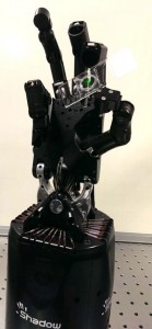
The NPL March 27, 2014 news release, which originated the news item, is accompanied by a rather interesting image,

A computer operated dexterous robotic hand holding a microscope slide with a fluorescent human cell (not to scale) embedded into a synthetic extracellular matrix. Courtesy: NPL

A computer operated dexterous
robotic hand holding a microscope
slide with a fluorescent human cell
(not to scale) embedded into a
synthetic extracellular matrix. Courtesy: NPL

The news release goes on to describe the BioTouch project in more detail (Note: A link has been removed),

The project will probe sensing and application of force and related vectors specific to biological self-assembly as a means of synthetic biology and nanoscale construction. The overarching objective is to enable the re-programming of self-assembled patterns and objects by directed micro-to-nano manipulation with compliant robotic haptic control.

This joint venture, funded by the European Research Council, EPSRC and NPL’s Strategic Research Programme, is a rare blend of interdisciplinary research bringing together expertise in robotics, haptics and machine vision with synthetic and cell biology, protein design, and super- and high-resolution microscopy. The research builds on the NPL’s pioneering developments in bioengineering and imaging and world-leading haptics technologies from UCL and MIT.

Haptics is an emerging enabling tool for sensing and manipulation through touch, which holds particular promise for the development of autonomous robots that need to perform human-like functions in unstructured environments. However, the path to all such applications is hampered by the lack of a compliant interface between a predictably assembled biological system and a human user. This research will enable human directed micro-manipulation of experimental biological systems using cutting-edge robotic systems and haptic feedback.

Recently the UK government has announced ‘eight great technologies’ in which Britain is to become a world leader. Robotics, synthetic biology, regenerative medicine and advanced materials are four of these technologies for which this project serves as a merging point providing thus an excellent example of how multidisciplinary collaborative research can shape our future.

If it read this rightly, it means they’re trying to design systems where robots will work directly with materials in the labs while humans direct the robots’ actions from a remote location. My best example of this (it’s not a laboratory example) would be of a surgery where a robot actually performs the work while a human directs the robot’s actions based on haptic (touch) information the human receives from the robot. Surgeons don’t necessarily see what they’re dealing with, they may be feeling it with their fingers (haptic information). In effect, the robot’s hands become an extension of the surgeon’s hands. I imagine using a robot’s ‘hands’ would allow for less invasive procedures to be performed.

Wilkinson Prize for numerical software: call for 2015 submissions

The Wilkinson Prize is not meant to recognize a nice, shiny new algorithm, rather it’s meant for the implementation phase and, as anyone who have ever been involved in that phase of a project can tell you, that phase is often sadly neglected. So, bravo for the Wilkinson Prize!

From the March 27, 2014 Numerical Algorithms Group (NAG) news release, here’s a brief history of the Wilkinson Prize,

Every four years the Numerical Algorithms Group (NAG), the National Physical Laboratory (NPL) and Argonne National Laboratory award the prestigious Wilkinson Prize in honour of the outstanding contributions of Dr James Hardy Wilkinson to the field of numerical software. The next Wilkinson Prize will be awarded at the [2015] International Congress on Industrial and Applied Mathematics in Beijing, and will consist of a $3000 cash prize.

NAG, NPL [UK National Physical Laboratory] and Argonne [US Dept. of Energy, Argonne National Laboratory] are committed to encouraging innovative, insightful and original work in numerical software in the same way that Wilkinson inspired many throughout his career. Wilkinson worked on the Automatic Computing Engine (ACE) while at NPL and later authored numerous papers on his speciality, numerical analysis. He also authored many of the routines for matrix computation in the early marks of the NAG Library.

The most recent Wilkinson Prize was awarded in 2011 to Andreas Waechter and Carl D. Laird for IPOPT. Commenting on winning the Wilkinson Prize Carl D. Laird, Associate Professor at the School of Chemical Engineering, Purdue University, said “I love writing software, and working with Andreas on IPOPT was a highlight of my career. From the beginning, our goal was to produce great software that would be used by other researchers and provide solutions to real engineering and scientific problems.

The Wilkinson Prize is one of the few awards that recognises the importance of implementation – that you need more than a great algorithm to produce high-impact numerical software. It rewards the tremendous effort required to ensure reliability, efficiency, and usability of the software.

Here’s more about the prize (list of previous winners, eligibility, etc.), from the Wilkinson Prize for Numerical Software call for submissions webpage,

Previous Prize winners:

  • 2011: Andreas Waechter and Carl D. Laird for Ipopt
  • 2007: Wolfgang Bangerth for deal.II
  • 2003: Jonathan Shewchuch for Triangle
  • 1999: Matteo Frigo and Steven Johnson for FFTW.
  • 1995: Chris Bischof and Alan Carle for ADIFOR 2.0.
  • 1991: Linda Petzold for DASSL.

Eligibility

The prize will be awarded to the authors of an outstanding piece of numerical software, or to individuals who have made an outstanding contribution to an existing piece of numerical software. In the latter case applicants must clearly be able to distinguish their personal contribution and to have that contribution authenticated, and the submission must be written in terms of that personal contribution and not of the software as a whole. To encourage researchers in the earlier stages of their career all applicants must be at most 40 years of age on January 1, 2014.
Rules for Submission

Each entry must contain the following:

Software written in a widely available high-level programming language.
A two-page summary of the main features of the algorithm and software implementation.
A paper describing the algorithm and the software implementation. The paper should give an analysis of the algorithm and indicate any special programming features.
Documentation of the software which describes its purpose and method of use.
Examples of use of the software, including a test program and data.

Submissions

The preferred format for submissions is a gzipped, tar archive or a zip file. Please contact us if you would like to use a different submission mechanism. Submissions should include a README file describing the contents of the archive and scripts for executing the test programs. Submissions can be sent by email to wilkinson-prize@nag.co.uk. Contact this address for further information.

The closing date for submissions is July 1, 2014.

Good luck to you all!

Graphene bits from the UK’s National Physical Laboratory and Cientifica

In the first bit of this week’s graphene news, the UK”s National Physical Laboratory (NPL) has joined the Graphene Stakeholders Association according to an Aug. 5, 2013 NPL news release,

The National Physical Laboratory (NPL) has joined the Graphene Stakeholders Association (GSA) as a lifetime member. NPL will work closely with the GSA to promote the responsible development of graphene and graphene-enabled technologies and applications.

“We foresee a significant role for NPL in the GSA in helping to develop common and accepted nomenclature, definitions, standard metrology and testing methods that will help foster and facilitate the development of graphene and graphene-enabled applications globally,” stated GSA co-founder, Stephen Waite. “We are delighted with NPL’s decision to join the GSA and look forward to working closely with Andrew Pollard and his colleagues in the months and years ahead,” says Waite.

NPL’s Andrew Pollard, who joins the GSA’s Advisory Board, said: “NPL has a leading role in the development of measurement techniques and international standards for graphene and 2-D materials, and the formation of the GSA is extremely well-timed as graphene progresses from the research laboratory to commercialisation. This partnership between two organisations with such well-aligned aims should enable the widely-predicted growth of a global graphene industry.”

I mentioned the founding of the Graphene Stakeholders Association in an April 23, 2013 posting. At the time I noted the group’s very interesting Graphene Industry Information page, which features these tidbits,

China has published more graphene patents than any other country, at 2,204, ahead of 1,754 for the U.S., 1,160 for South Korea, and 54 for the U.K.

South Korea’s Samsung has more graphene patents than any single company.

Nokia is part of the 74-company Graphene Flagship Consortium that is receiving a €1 billion ($1.35 billion) grant that the E.U. announced in January 2013.

Nokia, Philips, U.K. invention stalwart Dyson, weapons and aerospace company BAE Systems, and others have committed £13 million ($20.5 million) to a graphene development center [Cambridge Graphene Centre as per my Jan. 24, 2013 posting] at Cambridge University, to go along with £12 million ($18.9 million) from the British government. [Also, there’s a new National Graphene Institute being built in Manchester, UK {my Jan. 14, 2013 posting}.]

….

Graphene is prohibitively expensive to make today. As recently as 2008, it cost $100 million to produce a single cubic centimeter of graphene.

Researchers are working on methods to reduce the cost of manufacturing and help make graphene a ubiquitous fabrication material.

Graphene film companies face major commercialization hurdles, including reducing costs, scaling-up the substrate transfer process, overcoming current deposition area limitations, and besting other emerging material solutions.

This leads to the 2nd bit of graphene news, Cientifica (a business consultancy focusing on emerging technologies) has released its Graphene Opportunity Report, from the report’s webpage (Note: Links have been removed),

A decade ago when we published the first edition of the Nanotechnology Opportunity Report, there were predictions of untold riches for early investors, the replacement of all manufacturing as we know it, and the mythical trillion-dollar market.

Cientifica went against the grain by predicting that it would be hard for anyone to make money from nanomaterials, and that the real value would be in the applications. This has been borne out by the failure of even large global companies such as Mitsubishi Chemical and Bayer to make much headway with fullerenes and carbon nanotubes, and the failure of countless smaller nanomaterials producers.

On the other hand companies making use of nanomaterials, Germany’s Magforce Technologies and the US based BIND Therapeutics have shown what can be achieved when nanomaterials are applied to large addressable markets, in this case drug delivery.

Is Graphene The New Nanotech?

A similar amount of hype currently surrounds graphene, with wild predictions of applications ranging from microelectronics to water
treatment. This report examines these claims and taking the rational approach for which Cientifica is known, considers how valid these are and evaluates the chances of success.

We also look in detail at the graphene producers. Graphene comes in a wide range of forms, each with its own particular set of addressable applications. No one producer covers all applications and many are destined to be niche players. As with nanomaterials, many companies currently producing graphene are destined to burn brightly and then be unceremoniously snuffed out when scale up or access to applications fails to materialise.

..

As with all Cientifica reports, we look beyond the hype and take a rational and dispassionate look at the entire graphene value chain, from graphite to THz electronics. There will be long-term winners, and we indicate what strategies are required to join this small elite band, and we provide a wealth of lessons from our previous experience in nanotechnologies and life sciences.

Most importantly, we look beyond the narrow graphene or nanotechnology worlds and assess graphene’s chances of success in competing with a wide range of other technologies, many of which have not been considered by those concentrating solely on graphene.

The Graphene Opportunity Report is available at GBP 2000/EUR 2300/USD 3000.

You can access the report’s Table of Contents here.

‘Silverized’ clothing and wearable electronics

A July 30, 2013 news item on ScienceDaily features a technique for printing silver directly onto fibres,

Scientists at the National Physical Laboratory (NPL), the UK’s National Measurement Institute, have developed a way to print silver directly onto fibres. This new technique could make integrating electronics into all types of clothing simple and practical. This has many potential applications in sports, health, medicine, consumer electronics and fashion.

Most current plans for wearable electronics require weaving conductive materials into fabrics, which offer limited flexibility and can only be achieved when integrated into the design of the clothing from the start. [emphasis mine] NPL’s technique could allow lightweight circuits to be printed directly onto complete garments.

The July 30, 2013 National Physical Laboratory news release on EurekAlert, which originated the news item, provides a little more detail,

Silver coated fibres created using this technique are flexible and stretchable, meaning circuits can be easily printed onto many different types of fabric, including wool which is knitted in tight loops.

The technique involves chemically bonding a nano‐silver layer onto individual fibres to a thickness of 20 nm. The conductive silver layer fully encapsulates fibres and has good adhesion and excellent conductivity.

The researchers don’t appear to have published a paper but there is a bit more information on the NPL’s Smart Textiles webpage,

At NPL the Electronics Interconnection group has developed a new method to produce conductive textiles. This new technique could make integrating electronics into all types of clothing simple and practical by enabling lightweight circuits to be printed directly onto complete garments.

The nano silver material is chemically bonded to the fabric, encapsulating the fibres and providing full coverage. The resulting textile demonstrates good adhesion, flexibility and is stretchable achieving excellent resistivity of 0.2 Ω/sq.

My May 9, 2012 posting concerns a project where batteries were being woven into textiles for the US military.

Honey, could you please unzip my electronics?

The UK’s National Physical Laboratory has been proceeding with an interesting project on reusable electronics, ReUSE (Reuseable, Unzippable, Sustainable Electronics), according to the Oct. 30, 2012 news item on Nanowerk,

The National Physical Laboratory (NPL), along with partners In2Tec Ltd (UK) and Gwent Electronic Materials Ltd, have developed a printed circuit board (PCB) whose components can be easily separated by immersion in hot water. …

The electronics industry has a waste problem – currently over 100 million electronic units are discarded annually in the UK alone, making it one of the fastest growing waste streams.


It was estimated in a DTI [Dept. of Trade and Industry]-funded report, that around 85% of all PCB scrap board waste goes to landfill. Around 70% of this being of non-metallic content with little opportunity for recycling. This amounts to around 1 million tonnes in the UK annually equivalent to 81 x HMS Belfasts [ships]

This revolutionary materials technology allows a staggering 90% of the original structure to be re-used. For comparison, less than 2% of traditional PCB material can be re-used. The developed technology lends itself readily to rigid, flexible and 3D structures, which will enable the electronics industry to pursue new design philosophies – with the emphasis on using less materials and improving sustainability.

Here’s a video demonstrating the technology, from the ReUSE project news page,

I had to look at this twice to confirm what I was seeing. (I worked for a company that manufactured circuit boards for its products and the idea of immersing one of those in hot water is pretty shocking to me [pun intended].)